AM3407-V1.0
LM4040_05中文资料
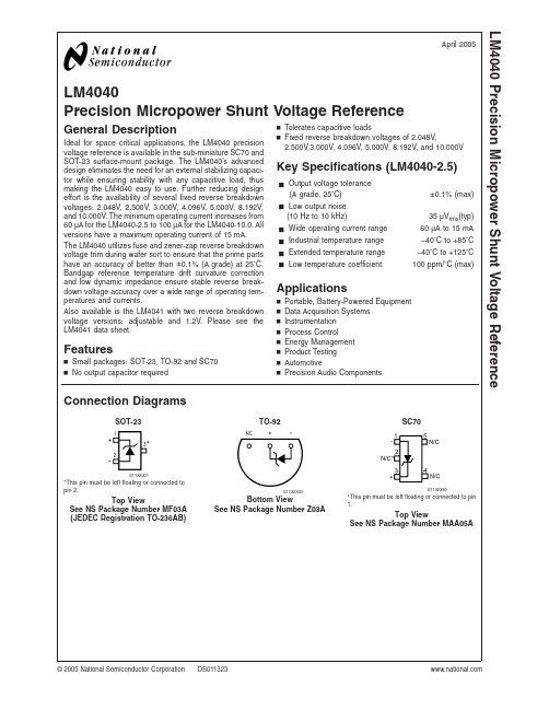
LM4040Precision Micropower Shunt Voltage ReferenceGeneral DescriptionIdeal for space critical applications,the LM4040precision voltage reference is available in the sub-miniature SC70and SOT-23surface-mount package.The LM4040’s advanced design eliminates the need for an external stabilizing capaci-tor while ensuring stability with any capacitive load,thus making the LM4040easy to use.Further reducing design effort is the availability of several fixed reverse breakdown voltages:2.048V,2.500V,3.000V,4.096V,5.000V,8.192V,and 10.000V.The minimum operating current increases from 60µA for the LM4040-2.5to 100µA for the LM4040-10.0.All versions have a maximum operating current of 15mA.The LM4040utilizes fuse and zener-zap reverse breakdown voltage trim during wafer sort to ensure that the prime parts have an accuracy of better than ±0.1%(A grade)at 25˚C.Bandgap reference temperature drift curvature correction and low dynamic impedance ensure stable reverse break-down voltage accuracy over a wide range of operating tem-peratures and currents.Also available is the LM4041with two reverse breakdown voltage versions:adjustable and 1.2V.Please see the LM4041data sheet.Featuresn Small packages:SOT-23,TO-92and SC70n No output capacitor requiredn Tolerates capacitive loadsn Fixed reverse breakdown voltages of 2.048V,2.500V,3.000V,4.096V,5.000V,8.192V,and 10.000VKey Specifications (LM4040-2.5)j Output voltage tolerance(A grade,25˚C)±0.1%(max)j Low output noise(10Hz to 10kHz)35µV rms (typ)j Wide operating current range 60µA to 15mA j Industrial temperature range −40˚C to +85˚C j Extended temperature range −40˚C to +125˚C j Low temperature coefficient100ppm/˚C (max)Applicationsn Portable,Battery-Powered Equipment n Data Acquisition Systems n Instrumentation n Process Controln Energy Management n Product Testing n AutomotivenPrecision Audio ComponentsConnection DiagramsSOT-23TO-92SC7001132301*This pin must be left floating or connected to pin 2.Top ViewSee NS Package Number MF03A (JEDEC Registration TO-236AB)01132303Bottom ViewSee NS Package Number Z03A01132330*This pin must be left floating or connected to pin1.Top ViewSee NS Package Number MAA05AApril 2005LM4040Precision Micropower Shunt Voltage Reference©2005National Semiconductor Corporation Ordering InformationIndustrial Temperature Range (−40˚C to +85˚C)Reverse Breakdown Voltage Tolerance at 25˚C and Average Reverse Breakdown Voltage Temperature CoefficientPackageNS Package NumberM3(SOT-23)M7(SC70)Z (TO-92)Supplied as 1000Units Tape andReelSupplied as 3000Units tape andReelSupplied as 1000Units Tape andReelSupplied as 3000Units Tape andReel±0.1%,100ppm/˚C max (A grade)LM4040AIM3-2.0LM4040AIM3-2.5LM4040AIM3-3.0LM4040AIM3-4.1LM4040AIM3-5.0LM4040AIM3-8.2LM4040AIM3-10.0LM4040AIM3X-2.0LM4040AIM3X-2.5LM4040AIM3X-3.0LM4040AIM3X-4.1LM4040AIM3X-5.0LM4040AIM3X-8.2LM4040AIM3X-10.0LM4040AIZ-2.0LM4040AIZ-2.5LM4040AIZ-3.0LM4040AIZ-4.1LM4040AIZ-5.0LM4040AIZ-8.2LM4040AIZ-10.0MF03A,Z03A±0.2%,100ppm/˚C max (B grade)LM4040BIM3-2.0LM4040BIM3-2.5LM4040BIM3-3.0LM4040BIM3-4.1LM4040BIM3-5.0LM4040BIM3-8.2LM4040BIM3-10.0LM4040BIM3X-2.0LM4040BIM3X-2.5LM4040BIM3X-3.0LM4040BIM3X-4.1LM4040BIM3X-5.0LM4040BIM3X-8.2LM4040BIM3X-10.0LM4040BIM7-2.0LM4040BIM7-2.5LM4040BIM7-3.0LM4040BIM7-4.1LM4040BIM7-5.0LM4040BIM7X-2.0LM4040BIM7X-2.5LM4040BIM7X-3.0LM4040BIM7X-4.1LM4040BIM7X-5.0LM4040BIZ-2.0LM4040BIZ-2.5LM4040BIZ-3.0LM4040BIZ-4.1LM4040BIZ-5.0LM4040BIZ-8.2LM4040BIZ-10.0MF03A,Z03A,MAA05A ±0.5%,100ppm/˚C max (C grade)LM4040CIM3-2.0LM4040CIM3-2.5LM4040CIM3-3.0LM4040CIM3-4.1LM4040CIM3-5.0LM4040CIM3-8.2LM4040CIM3-10.0LM4040CIM3X-2.0LM4040CIM3X-2.5LM4040CIM3X-3.0LM4040CIM3X-4.1LM4040CIM3X-5.0LM4040CIM3X-8.2LM4040CIM3X-10.0LM4040CIM7-2.0LM4040CIM7-2.5LM4040CIM7-3.0LM4040CIM7-4.1LM4040CIM7-5.0LM4040CIM7X-2.0LM4040CIM7X-2.5LM4040CIM7X-3.0LM4040CIM7X-4.1LM4040CIM7X-5.0LM4040CIZ-2.0LM4040CIZ-2.5LM4040CIZ-3.0LM4040CIZ-4.1LM4040CIZ-5.0LM4040CIZ-8.2LM4040CIZ-10.0MF03A,Z03A,MAA05A ±1.0%,150ppm/˚C max (D grade)LM4040DIM3-2.0LM4040DIM3-2.5LM4040DIM3-3.0LM4040DIM3-4.1LM4040DIM3-5.0LM4040DIM3-8.2LM4040DIM3-10.0LM4040DIM3X-2.0LM4040DIM3X-2.5LM4040DIM3X-3.0LM4040DIM3X-4.1LM4040DIM3X-5.0LM4040DIM3X-8.2LM4040DIM3X-10.0LM4040DIM7-2.0LM4040DIM7-2.5LM4040DIM7-3.0LM4040DIM7-4.1LM4040DIM7-5.0LM4040DIM7X-2.0LM4040DIM7X-2.5LM4040DIM7X-3.0LM4040DIM7X-4.1LM4040DIM7X-5.0LM4040DIZ-2.0LM4040DIZ-2.5LM4040DIZ-3.0LM4040DIZ-4.1LM4040DIZ-5.0LM4040DIZ-8.2LM4040DIZ-10.0MF03A,Z03A,MAA05A ±2.0%,150ppm/˚C max (E grade)LM4040EIM3-2.0LM4040EIM3-2.5LM4040EIM3-3.0LM4040EIM3X-2.0LM4040EIM3X-2.5LM4040EIM3X-3.0LM4040EIM7-2.0LM4040EIM7-2.5LM4040EIM7-3.0LM4040EIM7X-2.0LM4040EIM7X-2.5LM4040EIM7X-3.0LM4040EIZ-2.0LM4040EIZ-2.5LM4040EIZ-3.0MF03A,Z03A,MAA05AL M 4040 2Extended Temperature Range(−40˚C to+125˚C)Reverse BreakdownVoltage Tolerance at25˚C and Average Reverse Breakdown Voltage Temperature CoefficientPackageM3(SOT-23) See NS Package Number MF03A±0.5%,100ppm/˚C max(C grade)LM4040CEM3-2.0,LM4040CEM3-2.5,LM4040CEM3-3.0,LM4040CEM3-5.0±1.0%,150ppm/˚C max(D grade)LM4040DEM3-2.0,LM4040DEM3-2.5,LM4040DEM3-3.0,LM4040DEM3-5.0±2.0%,150ppm/˚C max(E grade)LM4040EEM3-2.0,LM4040EEM3-2.5,LM4040EEM3-3.0LM40403SOT-23AND SC70Package Marking InformationOnly three fields of marking are possible on the SOT-23’s and SC70’s small surface.This table gives the meaning of the three fields.Part Marking Field DefinitionRJA SOT-23only First Field:R2A SOT-23only RKA SOT-23only R4A SOT-23only R =Reference R5A SOT-23onlySecond Field:J =2.048V Voltage Option 2=2.500V Voltage OptionR8A SOT-23only K =3.000V Voltage Option R0A SOT-23only4=4.096V Voltage Option RJB R2B 5=5.000V Voltage Option RKB R4B 8=8.192V Voltage Option R5B 0=10.000V Voltage Option R8B SOT-23only R0B SOT-23onlyThird Field:RJC R2C A–E =Initial Reverse Breakdown Voltage or Reference Voltage Tolerance RKC R4C A =±0.1%,B =±0.2%,C =+0.5%,D =±1.0%,E =±2.0%R5C R8C SOT-23only R0C SOT-23onlyRJD R2D RKD R4D R5D R8D SOT-23only R0D SOT-23onlyRJE R2E RKEL M 4040 4Absolute Maximum Ratings(Note1)If Military/Aerospace specified devices are required, please contact the National Semiconductor Sales Office/ Distributors for availability and specifications. Reverse Current20mA Forward Current10mA Power Dissipation(T A=25˚C)(Note2)M3Package306mW Z Package550mW M7Package241mW Storage Temperature−65˚C to+150˚C Lead TemperatureM3PackageVapor phase(60seconds)+215˚C Infrared(15seconds)+220˚C Z PackageSoldering(10seconds)+260˚C ESD SusceptibilityHuman Body Model(Note3)2kVMachine Model(Note3)200V See AN-450“Surface Mounting Methods and Their Effect on Product Reliability”for other methods of soldering surface mount devices.Operating Ratings(Notes1,2) Temperature Range(T min≤T A≤T max) Industrial Temperature Range−40˚C≤T A≤+85˚C Extended Temperature Range−40˚C≤T A≤+125˚C Reverse CurrentLM4040-2.060µA to15mA LM4040-2.560µA to15mA LM4040-3.062µA to15mA LM4040-4.168µA to15mA LM4040-5.074µA to15mA LM4040-8.291µA to15mA LM4040-10.0100µA to15mALM4040-2.0Electrical Characteristics(Industrial Temperature Range)Boldface limits apply for T A=T J=T MIN to T MAX;all other limits T A=T J=25˚C.The grades A and B designate initial Re-verse Breakdown Voltage tolerances of±0.1%and±0.2%,respectively.Symbol Parameter Conditions Typical(Note4)LM4040AIM3LM4040AIZ(Limit)(Note5)LM4040BIM3LM4040BIZLM4040BIM7(Limit)(Note5)Units(Limit)V R Reverse Breakdown Voltage I R=100µA 2.048VReverse Breakdown Voltage Tolerance(Note6)I R=100µA±2.0±4.1mV(max)±15±17mV(max)I RMIN Minimum Operating Current45µA6060µA(max)6565µA(max)∆V R/∆T Average Reverse BreakdownVoltage TemperatureCoefficient(Note6)I R=10mA±20ppm/˚CI R=1mA±15±100±100ppm/˚C(max) I R=100µA±15ppm/˚C∆V R/∆I R Reverse Breakdown VoltageChange with OperatingCurrent Change(Note*NOTARGET FOR*)I RMIN≤I R≤1mA0.3mV0.80.8mV(max)1.0 1.0mV(max) 1mA≤I R≤15mA2.5mV6.0 6.0mV(max)8.08.0mV(max)Z R Reverse DynamicImpedance I R=1mA,f=120Hz,I AC=0.1I R0.3Ω0.80.8Ω(max)e N Wideband Noise I R=100µA35µV rms10Hz≤f≤10kHzLM40405LM4040-2.0Electrical Characteristics (Industrial Temperature Range)(Continued)Boldface limits apply for T A =T J =T MIN to T MAX ;all other limits T A =T J =25˚C.The grades A and B designate initial Re-verse Breakdown Voltage tolerances of ±0.1%and ±0.2%,respectively.Symbol Parameter ConditionsTypical (Note 4)LM4040AIM3LM4040AIZ (Limit)(Note 5)LM4040BIM3LM4040BIZ LM4040BIM7(Limit)(Note 5)Units (Limit)∆V RReverse Breakdown Voltage Long Term Stability t =1000hrs T =25˚C ±0.1˚CI R =100µA 120ppmV HYSTThermal Hysteresis (Note 8)∆T =−40˚C to +125˚C0.08%LM4040-2.0Electrical Characteristics (Industrial Temperature Range)Boldface limits apply for T A =T J =T MIN to T MAX ;all other limits T A =T J =25˚C.The grades C,D and E designate initial Reverse Breakdown Voltage tolerances of ±0.5%,±1.0%and ±2.0%,respectively.SymbolParameterConditionsTypical (Note 4)LM4040CIM3LM4040CIZ LM4040CIM7(Limit)(Note 5)LM4040DIM3LM4040DIZ LM4040DIM7(Limit)(Note 5)LM4040EIM7LM4040EIZ (Limit)(Note 5)Units(Limit)V RReverse Breakdown VoltageI R =100µA 2.048VReverse Breakdown Voltage Tolerance (Note 6)I R =100µA ±10±20±41mV (max)±23±40±60mV (max)I RMINMinimum Operating Current45µA 606565µA (max)657070µA (max)∆V R /∆TAverage Reverse Breakdown Voltage Temperature Coefficient (Note 6)I R =10mA ±20ppm/˚CI R =1mA ±15±100±150±150ppm/˚C (max)I R =100µA±15ppm/˚C ∆V R /∆I RReverse Breakdown Voltage Change with Operating Current Change (Note *NO TARGET FOR *)I RMIN ≤I R ≤1mA 0.3mV 0.8 1.0 1.0mV (max)1.01.21.2mV (max)1mA ≤I R ≤15mA 2.5mV 6.08.08.0mV (max)8.010.010.0mV (max)Z R Reverse Dynamic Impedance I R =1mA,f =120Hz 0.3ΩI AC =0.1I R 0.91.11.1Ω(max)e N Wideband NoiseI R =100µA 35µV rms10Hz ≤f ≤10kHz∆V RReverse Breakdown Voltage Long Term Stability t =1000hrsT =25˚C ±0.1˚C 120ppmI R =100µA V HYSTThermal Hysteresis (Note 8)∆T =−40˚C to +125˚C0.08%L M 4040 6LM4040-2.0Electrical Characteristics(Extended Temperature Range)Boldface limits apply for T A=T J=T MIN to T MAX;all other limits T A=T J=25˚C.The grades C,D and E designate initial Reverse Breakdown Voltage tolerances of±0.5%,±1.0%and±2.0%,respectively.Symbol Parameter Conditions Typical(Note4)LM4040CEM3(Limit)(Note5)LM4040DEM3(Limit)(Note5)LM4040EEM3(Limit)(Note5)Units(Limit)V R Reverse BreakdownVoltageI R=100µA 2.048VReverse Breakdown Voltage Tolerance (Note6)I R=100µA±10±20±41mV(max)±30±50±70mV(max)I RMIN Minimum OperatingCurrent 45µA606565µA(max)687373µA(max)∆V R/∆T Average ReverseBreakdown VoltageTemperatureCoefficient(Note6)I R=10mA±20ppm/˚CI R=1mA±15±100±150±150ppm/˚C(max) I R=100µA±15ppm/˚C∆V R/∆I R Reverse BreakdownVoltage Change withOperating CurrentChange(Note7)I RMIN≤I R≤1mA0.3mV0.8 1.0 1.0mV(max)1.0 1.2 1.2mV(max) 1mA≤I R≤15mA2.5mV6.08.08.0mV(max)8.010.010.0mV(max)Z R Reverse DynamicImpedance I R=1mA,f=120Hz,I AC=0.1I R0.3Ω0.9 1.1 1.1Ω(max)e N Wideband Noise I R=100µA35µV rms10Hz≤f≤10kHz∆V R Reverse BreakdownVoltage Long TermStability t=1000hrsT=25˚C±0.1˚CI R=100µA120ppmV HYST Thermal Hysteresis(Note8)∆T=−40˚C to+125˚C0.08%LM4040-2.5Electrical Characteristics(Industrial Temperature Range)Boldface limits apply for T A=T J=T MIN to T MAX;all other limits T A=T J=25˚C.The grades A and B designate initial Re-verse Breakdown Voltage tolerances of±0.1%and±0.2%,respectively.Symbol Parameter Conditions Typical(Note4)LM4040AIM3LM4040AIZ(Limit)(Note5)LM4040BIM3LM4040BIZLM4040BIM7Limits(Note5)Units(Limit)V R Reverse Breakdown Voltage I R=100µA 2.500VReverse Breakdown Voltage Tolerance(Note6)I R=100µA±2.5±5.0mV(max)±19±21mV(max)I RMIN Minimum Operating Current45µA6060µA(max)6565µA(max)LM40407LM4040-2.5Electrical Characteristics (Industrial Temperature Range)(Continued)Boldface limits apply for T A =T J =T MIN to T MAX ;all other limits T A =T J =25˚C.The grades A and B designate initial Re-verse Breakdown Voltage tolerances of ±0.1%and ±0.2%,respectively.Symbol Parameter ConditionsTypical (Note 4)LM4040AIM3LM4040AIZ (Limit)(Note 5)LM4040BIM3LM4040BIZ LM4040BIM7Limits (Note 5)Units (Limit)∆V R /∆TAverage Reverse Breakdown Voltage Temperature Coefficient (Note 6)I R =10mA ±20ppm/˚CI R =1mA ±15±100±100ppm/˚C (max)I R =100µA±15ppm/˚C ∆V R /∆I R Reverse Breakdown Voltage Change with Operating Current Change (Note 7)I RMIN ≤I R ≤1mA0.3mV0.80.8mV (max)1.01.0mV (max)1mA ≤I R ≤15mA2.5mV 6.0 6.0mV (max)8.08.0mV (max)Z R Reverse Dynamic Impedance I R =1mA,f =120Hz,I AC =0.1I R 0.3Ω0.80.8Ω(max)e N Wideband NoiseI R =100µA 35µV rms10Hz ≤f ≤10kHz∆V RReverse Breakdown Voltage Long Term Stability t =1000hrs T =25˚C ±0.1˚CI R =100µA 120ppmV HYSTThermal Hysteresis (Note 8)∆T =−40˚C to +125˚C0.08%LM4040-2.5Electrical Characteristics (Industrial Temperature Range)Boldface limits apply for T A =T J =T MIN to T MAX ;all other limits T A =T J =25˚C.The grades C,D and E designate initial Reverse Breakdown Voltage tolerances of ±0.5%,±1.0%and ±2.0%,respectively.SymbolParameterConditionsTypical (Note 4)LM4040CIM3LM4040DIZ LM4040CIM7Limits (Note 5)LM4040DIM3LM4040DIZ LM4040DIM7Limits (Note 5)LM4040EIM7LM4040EIZ Limits(Note 5)Units(Limit)V RReverse Breakdown VoltageI R =100µA 2.500VReverse Breakdown Voltage Tolerance (Note 6)I R =100µA ±12±25±50mV (max)±29±49±74mV (max)I RMINMinimum Operating Current45µA 606565µA (max)657070µA (max)∆V R /∆TAverage Reverse Breakdown Voltage TemperatureCoefficient(Note 6)I R =10mA ±20ppm/˚C I R =1mA ±15±100±150±150ppm/˚C (max)I R =100µA±15ppm/˚CL M 4040 8LM4040-2.5Electrical Characteristics(Industrial Temperature Range)(Continued)Boldface limits apply for T A=T J=T MIN to T MAX;all other limits T A=T J=25˚C.The grades C,D and E designate initial Reverse Breakdown Voltage tolerances of±0.5%,±1.0%and±2.0%,respectively.Symbol Parameter Conditions Typical(Note4)LM4040CIM3LM4040DIZLM4040CIM7Limits(Note5)LM4040DIM3LM4040DIZLM4040DIM7Limits(Note5)LM4040EIM7LM4040EIZLimits(Note5)Units(Limit)∆V R/∆I R Reverse BreakdownVoltage Change withOperating CurrentChange(Note7)I RMIN≤I R≤1mA0.3mV0.8 1.0 1.0mV(max)1.0 1.2 1.2mV(max) 1mA≤I R≤15mA2.5mV6.08.08.0mV(max)8.010.010.0mV(max)Z R Reverse DynamicImpedance I R=1mA,f=120Hz0.3ΩI AC=0.1I R0.9 1.1 1.1Ω(max)e N Wideband Noise I R=100µA35µV rms10Hz≤f≤10kHz∆V R Reverse BreakdownVoltage Long TermStability t=1000hrsT=25˚C±0.1˚C120ppm I R=100µAV HYST Thermal Hysteresis(Note8)∆T=−40˚C to+125˚C0.08%LM4040-2.5Electrical Characteristics(Extended Temperature Range)Boldface limits apply for T A=T J=T MIN to T MAX;all other limits T A=T J=25˚C.The grades C,D and E designate initial Reverse Breakdown Voltage tolerances of±0.5%,±1.0%and±2.0%,respectively.Symbol Parameter Conditions Typical(Note4)LM4040CEM3Limits(Note5)LM4040DEM3Limits(Note5)LM4040EEM3Limits(Note5)Units(Limit)V R Reverse BreakdownVoltageI R=100µA 2.500VReverse Breakdown VoltageTolerance(Note6)I R=100µA±12±25±50mV(max)±38±63±88mV(max)I RMIN Minimum OperatingCurrent 45µA606565µA(max)687373µA(max)∆V R/∆T Average ReverseBreakdown VoltageTemperatureCoefficient(Note6)I R=10mA±20ppm/˚CI R=1mA±15±100±150±150ppm/˚C(max) I R=100µA±15ppm/˚C∆V R/∆I R Reverse BreakdownVoltage Change withOperating CurrentChange(Note7)I RMIN≤I R≤1mA0.3mV0.8 1.0 1.0mV(max)1.0 1.2 1.2mV(max)1mA≤I R≤15mA 2.5mV6.08.08.0mV(max)8.010.010.0mV(max)LM40409LM4040-2.5Electrical Characteristics (Extended Temperature Range)(Continued)Boldface limits apply for T A =T J =T MIN to T MAX ;all other limits T A =T J =25˚C.The grades C,D and E designate initial Reverse Breakdown Voltage tolerances of ±0.5%,±1.0%and ±2.0%,respectively.SymbolParameterConditionsTypical (Note 4)LM4040CEM3Limits (Note 5)LM4040DEM3Limits (Note 5)LM4040EEM3Limits (Note 5)Units(Limit)Z R Reverse Dynamic Impedance I R =1mA,f =120Hz,I AC =0.1I R 0.3Ω0.91.11.1Ω(max)e N Wideband NoiseI R =100µA 35µV rms10Hz ≤f ≤10kHz∆V RReverse Breakdown Voltage Long Term Stabilityt =1000hrsT =25˚C ±0.1˚CI R =100µA 120ppmV HYSTThermal Hysteresis(Note 8)∆T =−40˚C to +125˚C0.08%LM4040-3.0Electrical Characteristics (Industrial Temperature Range)Boldface limits apply for T A =T J =T MIN to T MAX ;all other limits T A =T J =25˚C.The grades A and B designate initial Re-verse Breakdown Voltage tolerances of ±0.1%and ±0.2%,respectively.Symbol Parameter ConditionsTypical (Note 4)LM4040AIM3LM4040AIZ (Limit)(Note 5)LM4040BIM3LM4040BIZ LM4040BIM7Limits (Note 5)Units (Limit)V R Reverse Breakdown Voltage I R =100µA 3.000VReverse Breakdown Voltage Tolerance (Note 6)I R =100µA ±3.0±6.0mV (max)±22±26mV (max)I RMINMinimum Operating Current47µA 6262µA (max)6767µA (max)∆V R /∆TAverage Reverse Breakdown Voltage Temperature Coefficient (Note 6)I R =10mA ±20ppm/˚C I R =1mA ±15±100±100ppm/˚C (max)I R =100µA±15ppm/˚C ∆V R /∆I R Reverse Breakdown Voltage Change with Operating Current Change (Note 7)I RMIN ≤I R ≤1mA0.6mV0.80.8mV (max)1.11.1mV (max)1mA ≤I R ≤15mA2.7mV 6.0 6.0mV (max)9.09.0mV (max)Z R Reverse Dynamic Impedance I R =1mA,f =120Hz,I AC =0.1I R 0.4Ω0.90.9Ω(max)e N Wideband NoiseI R =100µA 35µV rms10Hz ≤f ≤10kHz∆V RReverse Breakdown Voltage Long Term Stability t =1000hrs T =25˚C ±0.1˚CI R =100µA 120ppmV HYSTThermal Hysteresis (Note 8)∆T =−40˚C to +125˚C0.08%L M 4040 10LM4040-3.0Electrical Characteristics(Industrial Temperature Range)Boldface limits apply for T A=T J=T MIN to T MAX;all other limits T A=T J=25˚C.The grades C,D and E designate initial Reverse Breakdown Voltage tolerances of±0.5%,±1.0%and±2.0%,respectively.Symbol Parameter Conditions Typical(Note4)LM4040CIM3LM4040DIZLM4040CIM7Limits(Note5)LM4040DIM3LM4040DIZLM4040DIM7Limits(Note5)LM4040EIM7LM4040EIZLimits(Note5)Units(Limit)V R Reverse BreakdownVoltageI R=100µA 3.000VReverse Breakdown Voltage Tolerance (Note6)I R=100µA±15±30±60mV(max)±34±59±89mV(max)I RMIN Minimum OperatingCurrent 45µA606565µA(max)657070µA(max)∆V R/∆T Average ReverseBreakdown VoltageTemperatureCoefficient(Note6)I R=10mA±20ppm/˚CI R=1mA±15±100±150±150ppm/˚C(max) I R=100µA±15ppm/˚C∆V R/∆I R Reverse BreakdownVoltage Change withOperating CurrentChange(Note7)I RMIN≤I R≤1mA0.4mV0.8 1.1 1.1mV(max)1.1 1.3 1.3mV(max) 1mA≤I R≤15mA2.7mV6.08.08.0mV(max)9.011.011.0mV(max)Z R Reverse DynamicImpedance I R=1mA,f=120Hz0.4ΩI AC=0.1I R0.9 1.2 1.2Ω(max)e N Wideband Noise I R=100µA35µV rms10Hz≤f≤10kHz∆V R Reverse BreakdownVoltage Long TermStability t=1000hrsT=25˚C±0.1˚C120ppm I R=100µAV HYST Thermal Hysteresis(Note8)∆T=−40˚C to+125˚C0.08%LM4040-3.0Electrical Characteristics(Extended Temperature Range)Boldface limits apply for T A=T J=T MIN to T MAX;all other limits T A=T J=25˚C.The grades C,D and E designate initial Reverse Breakdown Voltage tolerances of±0.5%,±1.0%and±2.0%,respectively.Symbol Parameter Conditions Typical(Note4)LM4040CEM3Limits(Note5)LM4040DEM3Limits(Note5)LM4040EEM3Limits(Note5)Units(Limit)V R Reverse BreakdownVoltageI R=100µA 3.000VReverse Breakdown VoltageTolerance(Note6)I R=100µA±15±30±60mV(max)±45±75±105mV(max)I RMIN Minimum OperatingCurrent 47µA626767µA(max)707575µA(max)LM4040LM4040-3.0Electrical Characteristics (Extended Temperature Range)(Continued)Boldface limits apply for T A =T J =T MIN to T MAX ;all other limits T A =T J =25˚C.The grades C,D and E designate initial Reverse Breakdown Voltage tolerances of ±0.5%,±1.0%and ±2.0%,respectively.SymbolParameterConditionsTypical (Note 4)LM4040CEM3Limits (Note 5)LM4040DEM3Limits (Note 5)LM4040EEM3Limits (Note 5)Units(Limit)∆V R /∆TAverage Reverse Breakdown Voltage TemperatureCoefficient (Note 6)I R =10mA ±20ppm/˚CI R =1mA ±15±100±150±150ppm/˚C (max)I R =100µA±15ppm/˚C ∆V R /∆I R Reverse Breakdown Voltage Change with Operating Current Change (Note 7)I RMIN ≤I R ≤1mA0.4mV 0.8 1.1 1.1mV (max)1.11.31.3mV (max)1mA ≤I R ≤15mA2.7mV 6.08.08.0mV (max)9.011.011.0mV (max)Z R Reverse Dynamic Impedance I R =1mA,f =120Hz,I AC =0.1I R 0.4Ω0.91.21.2Ω(max)e N Wideband NoiseI R =100µA 35µV rms10Hz ≤f ≤10kHz∆V RReverse Breakdown Voltage Long Term Stabilityt =1000hrsT =25˚C ±0.1˚CI R =100µA 120ppmV HYSTThermal Hysteresis(Note 8)∆T =−40˚C to +125˚C0.08%LM4040-4.1Electrical Characteristics (Industrial Temperature Range)Boldface limits apply for T A =T J =T MIN to T MAX ;all other limits T A =T J =25˚C.The grades A and B designate initial Re-verse Breakdown Voltage tolerances of ±0.1%and ±0.2%,respectively.SymbolParameterConditionsTypical (Note 4)LM4040AIM3LM4040AIZ Limits (Note 5)LM4040BIM3LM4040BIZ LM4040BIM7Limits (Note 5)Units (Limit)V R Reverse Breakdown Voltage I R =100µA 4.096VReverse Breakdown Voltage Tolerance (Note 6)I R =100µA ±4.1±8.2mV (max)±31±35mV (max)I RMINMinimum Operating Current50µA 6868µA (max)7373µA (max)∆V R /∆TAverage Reverse Breakdown Voltage Temperature Coefficient(Note 6)I R =10mA ±30ppm/˚C I R =1mA ±20±100±100ppm/˚C (max)I R =100µA±20ppm/˚C ∆V R /∆I R Reverse Breakdown Voltage Change with Operating Current Change (Note 7)I RMIN ≤I R ≤1mA0.5mV0.90.9mV (max)1.21.2mV (max)1mA ≤I R ≤15mA3.0mV 7.07.0mV (max)10.010.0mV (max)L M 4040LM4040-4.1Electrical Characteristics(Industrial Temperature Range)(Continued)Boldface limits apply for T A=T J=T MIN to T MAX;all other limits T A=T J=25˚C.The grades A and B designate initial Re-verse Breakdown Voltage tolerances of±0.1%and±0.2%,respectively.Symbol Parameter Conditions Typical(Note4)LM4040AIM3LM4040AIZLimits(Note5)LM4040BIM3LM4040BIZLM4040BIM7Limits(Note5)Units(Limit)Z R Reverse DynamicImpedance I R=1mA,f=120Hz,0.5ΩI AC=0.1I R 1.0 1.0Ω(max)e N Wideband Noise I R=100µA80µV rms10Hz≤f≤10kHz∆V R Reverse Breakdown VoltageLong Term Stability t=1000hrsT=25˚C±0.1˚CI R=100µA120ppmV HYST Thermal Hysteresis(Note8)∆T=−40˚C to+125˚C0.08%LM4040LM4040-4.1Electrical Characteristics (Industrial Temperature Range)Boldface limits apply for T A =T J =T MIN to T MAX ;all other limits T A =T J =25˚C.The grades C and D designate initial Re-verse Breakdown Voltage tolerances of ±0.5%and ±1.0%,respectively.SymbolParameterConditionsTypical (Note 4)LM4040CIM3LM4040CIZ LM4040CIM7Limits (Note 5)LM4040DIM3LM4040BIZ LM4040DIM7Limits (Note 5)Units (Limit)V R Reverse Breakdown Voltage I R =100µA 4.096VReverse Breakdown Voltage Tolerance (Note 6)I R =100µA ±20±41mV (max)±47±81mV (max)I RMINMinimum Operating Current50µA 6873µA (max)7378µA (max)∆V R /∆T Average Reverse Breakdown Voltage Temperature Coefficient (Note 6)I R =10mA±30ppm/˚C I R =1mA ±20±100±150ppm/˚C (max)I R =100µA ±20ppm/˚C ∆V R /∆I R Reverse Breakdown Voltage Change with Operating Current Change (Note 7)I RMIN ≤I R ≤1mA 0.5mV0.9 1.2mV (max)1.21.5mV (max)1mA ≤I R ≤15mA3.0mV 7.09.0mV (max)10.013.0mV (max)Z R Reverse Dynamic Impedance I R =1mA,f =120Hz,0.5ΩI AC =0.1I R 1.01.3Ω(max)e N Wideband NoiseI R =100µA 80µV rms 10Hz ≤f ≤10kHz∆V RReverse Breakdown Voltage Long Term Stability t =1000hrs T =25˚C ±0.1˚CI R =100µA 120ppmV HYSTThermal Hysteresis (Note 8)∆T =−40˚C to +125˚C0.08%L M 4040LM4040-5.0Electrical Characteristics(Industrial Temperature Range)Boldface limits apply for T A=T J=T MIN to T MAX;all other limits T A=T J=25˚C.The grades A and B designate initial Re-verse Breakdown Voltage tolerances of±0.1%and±0.2%,respectively.Symbol Parameter Conditions Typical(Note4)LM4040AIM3LM4040AIZLimits(Note5)LM4040BIM3LM4040BIZLM4040BIM7Limits(Note5)Units(Limit)V R Reverse Breakdown Voltage I R=100µA 5.000VReverse Breakdown Voltage Tolerance(Note6)I R=100µA±5.0±10mV(max)±38±43mV(max)I RMIN Minimum Operating Current54µA7474µA(max)8080µA(max)∆V R/∆T Average Reverse Breakdown Voltage TemperatureCoefficient(Note6)I R=10mA±30ppm/˚CI R=1mA±20±100±100ppm/˚C(max) I R=100µA±20ppm/˚C∆V R/∆I R Reverse Breakdown VoltageChange with OperatingCurrent Change(Note7)I RMIN≤I R≤1mA0.5mV1.0 1.0mV(max)1.4 1.4mV(max) 1mA≤I R≤15mA 3.5mV8.08.0mV(max)12.012.0mV(max)Z R Reverse DynamicImpedance I R=1mA,f=120Hz,0.5ΩI AC=0.1I R 1.1 1.1Ω(max)e N Wideband Noise I R=100µA80µV rms10Hz≤f≤10kHz∆V R Reverse Breakdown VoltageLong Term Stability t=1000hrsT=25˚C±0.1˚C120ppm I R=100µAV HYST Thermal Hysteresis(Note8)∆T=−40˚C to+125˚C0.08%LM4040。
西门子变频器M430说明书
MICROMASTER 430
7.5 kW - 250 kW
使用说明书
版本 10/06
有关调试的
警告
!
¾ 未经培训合格的人员在变频器的器件/系统上工作或不遵守“警告”中的有关规定,就可能造
成严重的人身伤害或重大的财产损失。只有在设备的设计、安装、调试和运行方面受过培训 的经过认证合格的专业人员才允许在本设备的器件/系统上进行工作。
¾ 输入电源线只允许永久性紧固连接。设备必须接地(按照 IEC 536 Class 1、NEC 和其它适用 的标准)。
有关维修的
警告
!
¾ 设备的维修只能由西门子公司的服务部门,西门子公司授权的维修中心或经过认证合格并得
到授权的人员进行,这些人员应当十分熟悉本说明书中提出的所有警告和操作步骤。
¾ 任何有缺陷的部件和器件都必须用相应的备件更换。
¾ 在打开设备进行维修之前,一定要断开电源。
有关拆卸和废品处理的
注意 ¾ 变频器的包装箱是可以重复使用的。请保管好包装箱以备将来使用或把它返还给制造商。 ¾ 易卸螺丝和快速插接器便于您拆卸设备的部件。您可以回收这些拆卸下来的部件,并根据地
是其第§8 节关于“带电部件上工作时允许的安全距离”的规定。实际操作时,应该使用适当 的电子器具。 ¾ 在安装和调试变频器之前,请您务必仔细阅读这些安全规则和警告,以及设备上粘贴的所有 警示标志。确保警示标志置于醒目的地方,并更换已经脱落或损坏的标志。
MICROMASTER 430 使用说明书
矽力杰产品选型_恒佳兴电子专业电源IC

Single output step down (Buck) Converter Vin max < 7VSY8018A 2.5 5.5 0.45 / 0.6 ±2% 1.5 400/200 √Ultra Low Quiescent Current DFN2x2-8 SY8030L 2.5 5.5 0.6 2.25 0.6 ±1.5% 50 300/200 DFN2x2-6 SY8078B 1.85 5.5 0.6 3 0.4 ±2% 40 350/250 DFN1.45x1-6 SY8010 2.5 5.5 1 1.5 0.6 ±1.5% 50 200/150 DFN2x2-6 SY8011A 2.5 5.5 1 1.5 0.6 ±2% 40 230/150 DFN1.5x1.5-6 SY8061A 2.5 5.5 1 1.5 0.6 ±2% 60 260/170 Auto Discharge DFN2x2-6 SY8065L 2.5 5.5 1 1.5 0.6 ±2% 90 250/200 √SOT 23-6 SY8071 2.5 5.5 1 2 0.6 ±2% 40 260/170 SOT 23-5 SY8075 2.5 6.5 1 1.5 0.6 ±2% 40 260/170 DFN2x2-6 SY8077 2.5 6.5 1 1.5 0.6 ±2% 40 260/170 SOT 23-5 SY8080 2.5 5.5 1 3 0.6 ±2% 40 270/160 SOT 23-5SY8081 2.5 5.51 2.5 0.6 ±2%40230/150 Output auto discharge DFN1.5×1.5-6SY8011B 2.5 5.5 1.5 1.5 0.6 ±2%60210/130 DFN1.5x1.5-6SY8030 2.5 5.5 1.5 2.25 0.6 ±1.5%50200/150 Ext Mode DFN2x2-6 SY8002B 2.7 5.5 1.5 1 0.6 ±2% / 110/80 √Latch off protection SOT 23-6SY8002E 2.7 5.5 2 1 0.6 ±2% / 110/80 √Force PWM SOT 23-6SY8003L 2.7 5.5 2 1 0.6 ±2% 55 120/90 √DFN2x2-8Single output step down (Buck) Converter Vin max < 7V±2%SY8089 SOT 23-52.7 5.5 2 1 0.6 55 110/80 Latch off protectionSY8003C1 2.7 5.5 3 3 0.6 ±2% 55 110/80 √DFN2x2-8SY8823 2.5 5.5 3.5 2 0.6 ±1.5% 18 55/35 √QFN2x1.5-8SY8047 2.5 5.54 1.25 0.6 ±1.5%1875/55√QFN3x3-16SY8856 2.7 5.54 3 0.6 ±1.5%6035/15 √√DFN2x2-8√±1.5%SY8003F 2.7 5.5 3 1 0.6 / 110/80 DFN2x2-8 SY8079P 2.7 6.5 0.6 ±2% 55 125/95 Non latch off OVP SOT 23-6SY8032 2.7 5.5 2.5 0.6 ±2% 80 100/80 SOT 23-6SY8032E 2.7 5.5 2.5 0.6 ±2% 100/80 Force CCM SOT 23-6SY8003 2.7 5.5 0.6 ±2% 55 110/80 Latch SCP/OVP DFN2x2-8SY8003A 2.7 5.5 0.6 ±2% 55 110/80 Non-latch off protection DFN2x2-8SY8003C 2.7 5.5 0.6 ±2% 55 100/80 DFN2x2-8 SY8003E 2.7 5.5 0.6 ±2% 110/80 Force CCM DFN2x2-8 SY8043A 2.7 5.5 1.25 0.6 ±2% 18 75/55 DFN3x3-16 SY8047L 2.5 5.5 1.25 0.6 ±2% 18 75/55 QFN3x3-16 SY8859 2.7 5.5 0.6 ±1% 40 100/50 OVP/OCP/SCP/UVLO/OTP QFN1.5x1.5-7Single output step down (Buck) Converter Vin max < 7VPart Number Vin (min)(V)Vin (max)(V)Iout (max) (A) Fsw (MHz)Vout (min)( V)VoltageAcurracySY8824B 2.6 5.5 4 1.8 / ±1% SY8824C 2.6 5.5 4 1.8 / ±1% SY8035 2.7 5.5 5 1 0.6 ±1.5% SY8805A 3 5.5 5 1 0.6 ±1.5% SY8825 2.5 5.5 5 2 0.6 ±1.5% SY8876 2.7 6.5 6 1.2 0.6 ±1.5% SY8827K 2.5 5.5 6 2.4 ±1.5% SY8868 2.7 5.56 10.6 ±1% SY8099 2.7 5.5 6 1 0.6 ±1% SY8812 2.75 5.5 12 1 ±1%80 70/40Programmable Output Voltage: 0.7625Vto 1.55V in 12.5mV/step; Default 1.15Voutput voltage8015010018606550408070/4050/4035/1555/3538/1528/1735/1530/1212/6PackageTSOT 23-8Programmable Output Voltage: 0.7625Vto 1.55V in 12.5mV steps; Default 1.05Voutput voltageTSOT 23-8EXT SS DFN3x3-10DFN2x2-8QFN2x1.5-8OCP/UVLO/OTP DFN2x2-8I2C Programmable Vout: 0.7125V~ 1.5V CSP1.56x1.96-20in 12.5mV steps, Addr: 1000001xCOT mode,max dutyHigh efficiencyP rogrammable Output Voltage: 0.6V to1.5V in 10mV stepsQFN2x2-10TSOT 23-6QFN3x3-12Dual output step down (Buck) Converter Vin max < 7VPart Number Vin(min)(V)Vin(max)(V)Iout(max)(A)Fsw (MHz) Vout (min)(V)VoltageAcurracyQuiescentCurrent(uA)MO SFET Ron H/L (m? ) Power GoodOutputFeature/ Special Function PackageSY8020 2.5 5.5 1A x2 1.5 0.6 ±2% 50 200/150 Individual EN DFN3x3-12 SY8831 2.5 5.5 1A x2 1.5 0.6 ±2% 45/55 260/180 Individual EN TSOT 23-8 SY8832 2.5 5.5 2A x2 2 0.6 ±2% 35/45 125/100 Individual EN TSOT 23-8 SY8024 3 5.5 3A x2 1 0.6 ±2% 80 105/85 Individual EN DFN3x3-12 SY8821 2.5 5.5 1A/1.5A 2 0.6 ±2% 45 125/100 Individual EN DFN2x1.5-8Single output step down (Buck) Converter, Vin max > 7VuiescentOriginal Part Number Vin(min)(V)Vin(max)(V)Iout(max)(A)Fsw (MHz) Vout( imn)(V)Fixed O utputVoltage(V)VoltageAcurracyCurrent (uA)MOSFET(RonH/L) (m ? )Power oGodOutputFeature/ Special Function PackageSY8290 5 40 0.3 2 0.6 ±2.0% 160 2000/- SOT 23-6 SY8200 6 24 0.6 0.5 0.6 ±2% 400 420/200 SOT 23-6 SY8401 4.5 50 0.8 1.2 0.6 ±1.0% 150 700/- SOT 23-6SY8201 4.527 1 0.5 0.6 ±2%400350/150 SOT 23-6SY8201C 4.527 1 1.15 0.6 ±2%400350/150 Force CCM SOT 23-6SY85017 100 1 0.2~1MHz 1.2 ±2.0%400500/240 Programmable Switching Frequency SO8ESY8291 5 40 1.2 0.8 0.6 ±2.0% 160 180/- SOT 23-6 SY8502 7 100 1.8 0.2~1MHz 1.2 ±2.0% 400 500/240 Programmable Switching Frequency SO8ESingle output step down (Buck) Converter, Vin max > 7VVin(min) Vin(max) Iout(max) Fsw Vout(min) Voltage Quiescent MO SFET(Ron Power GoodPart Number(V) (V) Iout((m A)ax)(MHz) (V) Acurracy Current (uA) H/L) (m ? ) O utputFeature/ Special Function PackageSY8121 4.5 18 2 1 0.6 ±2% 400 170/160 SOT 23-6/ DFN2x2-6 SY8121B 4.35 18 2 1.2 0.6 ±2% 170/160 1.2MHz, FCCM SOT 23-6SY8120B1 4.5 18 2 0.5 0.6 ±2% 400 130/120 SOT 23-6SY8121C 4.5 18 2 1.2 0.6 ±2% 400 130/120 SOT 23-6SY8222 4.5 23 2 0.5 0.6 ±1.5% 400 150/110 √EXT SS, Hic-cup SCP DFN3x3-10SY8292 5 40 2 0.8 0.6 ±2.0% 160 180/- SOT 23-6SY8113B 4.5 18 3 0.5 0.6 ±1.5% 100 80/40 Hic-cup SCP TSOT 23-6SY8113C 4.518 3 1 0.6 ±1.5%10080/40 Hic-cup SCP TSOT 23-6SY8113D 4.5 18 3 0.5 0.6 ±1.5% 100 80/40 √Hic-cup SCP, EXT SS TSOT 23-8SY8113G 4.518 3 0.5 0.6 ±1.5%10080/40 Hic-cup SCP, FCCM TSOT 23-6SY8203A 4.523 3 1 0.6 ±1.5%400120/85 √EXT SS DFN3x3-10SY8223 4.523 3 0.5 0.6 ±1.5%400120/85 √EXT SS, Hic-cup SCP DFN3x3-10SY8253 4.5 23 3 0.5 0.6 ±1.5% 100 105/50 √EXT SS, Hic-cup SCP TSOT 23-8SY8303 4.5 40 3 0.5~2.5MHz 0.6 ±1.5% 18 70/110 TSOT 23-8 SY8293 5 40 3 0.8 0.6 ±2.0% 160 180/-SO8EPart Number Vin(min)(V)Vin(max)(V)Iout(max)(A)Fsw (MHz) Vout(min)(V)VoltageAcurracyQuiescentCurrent (uA)MO SFET(Ron H/L)(m ? )Power Good OutputFeature/ Special Function PackageSY8502 7 85 1.2 0.2~0.5 1.2 ±2.0% / 500/240 Programmable Switching FrequencyRangeSO8ESY8120B1 4.5 18 2 0.5 0.6 ±2% 400 130/120 SOT 23-6SY8121 4.5 18 2 1 0.6 ±2% 400 170/160 SOT 23-6/ DFN2x2-6 SY8121C 4.5 18 2 1.2 0.6 ±2% 400 130/120 SOT 23-6SY8222 4.5 23 2 0.5 0.6 ±1.5% 400 150/110 √EXT SS, Hic-cup SCP DFN3x3-10SY8292 5 40 2 0.8 0.6 ±2.0% 160 180/- SOT 23-6SY8113B 4.5 18 3 0.5 0.6 ±1.5% 100 80/40 Hic-cup SCP TSOT 23-6SY8113C 4.5 18 3 1 0.6 ±1.5% 100 80/40 Hic-cup SCP TSOT 23-6SY8113D 4.5 18 3 0.5 0.6 ±1.5% 100 80/40 √Hic-cup SCP, EXT SS TSOT 23-8SY8113G 4.5 18 3 0.5 0.6 ±1.5% 100 80/40 Hic-cup SCP, FCCM TSOT 23-6SY8203A 4.5 23 3 1 0.6 ±1.5% 400 120/85 √EXT SS DFN3x3-10SY8223 4.5 23 3 0.5 0.6 ±1.5% 400 120/85 √EXT SS, Hic-cup SCP DFN3x3-10SY8253 4.523 3 0.5 0.6 ±1.5%100105/50 √EXT SS, Hic-cup SCP TSOT 23-8SY8303 4.5 40 3 0.5~2.5MHz 0.6 ±1.5% 18 70/110 TSOT 23-8SY82935 40 3 0.8 0.6 ±2.0%160180/- SO8ESY8113H 4.5 18 3 0.5 0.6 ±1.5% 160 80/40 Programmable soft-start time TSOT 23-8±1.5%SY8104A4.518 4 0.5 0.6±1.5%100 50/30Instant PWM architectureSY8105 4.5 18 5 0.5 0.6±1.5%100 50/30SY8205 4.5 30 5 0.5 0.6±1.5%200 70/40√EXT SSSY8105A 4.5 18 5 0.5 0.6±1.5%100 40/20Instant PWM architectureSY8366H 4 28 6 0.8 0.6±1.5%100 40/20√Hic-cup SCP, 12A Peak current capability,programmable output current limitSY8286A 4 23 60.6 0.6 ±1.0% 12038/19 √SY8366K428 6 0.50.6±1.5%10040/20√Hic-cup SCP,6A continuous/12A peakoutput current capabilitySY8368A42880.80.6±1%100 20/10√Hic-cup SCP, 16A Peak current capability,programmable output current limitSY8288A 4 23 8 0.5 0.6 ±1.0% 80 30/10SY8288 4 23 8 0.5 0.6 ±1.0%8030/10SY8288C5.52380.60.6±1.5%10822/11√OVP/OCPSY8210A 4 28 10 0.6 0.6±1.5%300 25/8√Mem o ry power, 10A VDDQ/1A VTT LDO, 16A Peak Current capability, Latch offUVP/OVP, Over temperature alertSY8204 4.5 30 40.50.620080/50EXT SSPackageTSOT 23-6SO8ETSOT 23-6TSOT 23-6DFN3x4-12TSOT 23-6QFN3x3-12QFN3x3-20QFN3x3-12QFN3x3-12QFN3x3-20 QFN3x3-20QFN3x3-20QFN4x3-19Part Number Vin(min)(V)Vin(max)(V)Iout(max)(A)Fsw (MHz) Vout(min)(V) Voltage AcurracyQuiescent Current (uA)MO SFET(Ron H/L) (m ? ) Power Good OutputFeature/ Special Function Package SY8182 4 18 12 0.2~1MHz 0.6 ±1.0%18/6 √QFN4x4-20SY8182L 4.5 18 12 0.2~1MHz0.6 ±1.0% 500 18/6 √ Hic-cup SCP/OVPQFN4x4-24 SY8186418160.50.6±1.5%1507.5/2.5√Hic-cup SCP, programmble outputQFN4x4-11current limitPart NumberVin(min)(V)Vin(max)(V)Ilim (A)Fsw (MHz)Vout(max)(V)Sync BoostFixed O utputVoltage (V) Acu F r B ra /c y AcurracyInput Q uiescent Current (uA)Q uiescent current from output (uA)MO SFET Ro n (L/S) (m ? )Feature/ Special Function PackageSY7060L 0.7 5 0.2 / 5.25 Y /0.5V ±3% 0.518450/800SOT-363SY7070 0.7 5 0.35 / / Y 3.3 /0.5 5.5 500/700Bypass function @ shutdown SOT 23-5SY7070A 0.7 5 0.35 / / Y 3 / 0.5 5.5 500/700SOT 23-5SY7071 0.7 5 0.35 / 5.25 Y /1.0V ±3%0.5 5 500/700 Pass-through function @ shutdown SOT-363SY7071A 0.7 5 0.35 / / Y 5 / 0.5 7 400/500Pass-through function @ shutdown SOT-363SY7060 0.7 5 0.4 / 5.25 Y /0.5V ±3% 0.5 18 450/800SOT-363SY7080 0.9 4 1.8 1.2 4 Y / 1.2V ±3%65 / 90/200 Output Disconnect @Shutdown SOT 23-6Single output step Up (Boost) Converter (Low V oltage)Part NumberVin(min)(V)Vin(max)(V)Ilim (A)Fsw (MHz)Vout(max)(V)Sync BoostFixed O utput Voltage (V)Acu F rr B a /c y Acurracy InputQuiescent Current (uA) Quies cent current from output (uA) MOSFET Ron(L/S) (m ?) Feature/ Special Function PackageSY7063 1.8 5.25 3 0.5 5.5 Y / 1.2V ±1.5% 102736/40Output Disconnect @Shutdown QFN2x2-10SY7069 2.5 5.5 3 1 5.5 Y / 1.2V±1.5% 8 32 50/90TSOT 23-6SY7088 2.3 5 3 1 5.5 Y / 1.2V ±1.5% 2 30 70/85DFN2x3-8SY7088E 2.3 5 3 1 5.5 Y / 1.2V ±1.5% / / 70/85DFN2x3-8SY7065 1.8 5.25 5 0.5 5.5 Y / 1.2V ±1.5% 10 27 20/40 Auto output discharge function QFN2x2-10SY7065A 1.8 5.25 5 0.5 5.5 Y / 1.2V ±1.5% 10 27 20/40No output discharge function QFN2x2-10SY7076 2 5.5 6 0.5 5.5 Y / 1.2V ±1.5% 10 27 20/40QFN2x2-10SY7066 1.8 5.25 6 0.5 5.5 Y / 1.2V ±1.5% 10 27 20/40 Auto output discharge function QFN2x2-10SY7066B 1.8 5.25 6 0.5 5.5 Y / 1.2V ±1.5%10 27 20/40 Selectable Forced PWM mode QFN2x2-10Single output step Up (Boost) Converter (Low V oltage)SY9701A 2.6 5.5 1.2 1 5.5 0.6V ±1.5% 60 100/100 Output Disconnect @Shutdown DFN3x3-14Single output step Up (Boost) Converter (High Voltage)PackagePart NumberVin(min)(V)Vin(max)(V)Ilim (A)Fsw (MHz) Vout (max) (V) Sync BoostFB/ AcurracyInput Q uiescent Current (uA) MO SFET (RonMain/Rectified)(m? )Disconnect FET Ron ( m ?) Power Good OutputFeature/ Special FunctionSY7208C 3 25 0.6 1 25 N0.6V ±2%100 150/-Int SS/CompSOT 23-6SY7152A 3 8 2 1 16 N0.6V ±2%100 130/-Int SS/Comp SOT 23-6SY7208L 3 25 2 1 25 N0.6V ±2%100 150/-Int SS/Comp SOT 23-6SY7302 3 33 2 1 33 N0.6V ±2% 100 200/-Int SS/Comp SOT 23-6SY7388 3.5 30 2 0.85 30 N 1V ±2%150 200/-Accurate input current limit SOT 23-6SY7102 2 6 2.5 1 6 N0.6V ±2% 200 120/-Int SS/Comp SOT 23-6SY7801 2.5 5.5 2.5 1 / N 0.6V ±2%200 120/-Int SS, with 2A 80m? Load Switch DFN3x3-12SY7104A2 6 4 1 6 N0.6V ±2% 100 90/-Int SS/Comp DFN3x3-10SY7304 3334133N 0.6V ±2%100120/-QFN3x3-10SY7205 8.6 15.9 4.5 0.5 16 N1.25V±1.5% 120 75/-Adjustable soft-start time, OVP DFN3x3-10SY7982 3 9 6 1 13 Y 1V ±2% 600 80/4040√True shutdown QFN3x3-16SY7219 3 5.5 9 / 36 N 1.25V ±2%350 65/-EXT Comp DFN3x3-10 SY721531615/18Y1V ±1.5% 22016/1818√Int SS, OVP/SCP/ True shutdown ProgrammableSwitching Frequency: 0.2~1MHz QFN4x4-18SY7215A31615/18Y 1V ±1.5%2309/1212√Int SS, OVP/SCP/ True shutdown ProgrammableSwitching Frequency: 0.2~1MHzQFN4x4-181.23VInt SS; Adjustable current limit for optical module;SY7501B2.955.50.930.480N ±2%225 800/-Current limit indicator; Accurate high-side currentQFN3x3-16monitor; 320mW maximum output powerDC-DC PWM Controller (external Switch)Original Part Number Vin(min)(V)Vin(max)(V)Fsw (MHz)V(V R)EFFunction PackageSY7901 3 25 0.5 1 Current mode DC/DC controller targeted for Boost, Sepic, Flyback and Forward applications with DC Input Current Limit DFN3x3-10 SY7902A 3 25 0.3 1 Current mode DC/DC controller targeted for both Boost and Sepic applications with DC Output Current Limit SOP10 Power ModulePart Number Vin(min)(V)Vin(max)(V)Iout(max)(A)Fsw (MHz)Fixed O utputVoltage (V)Voltage Acurracy Q uiescent Current (uA) MOSFET (Ron H/L) (m? ) Integrated Inductor PackageSY98081 2.5 5.5 0.6 3 ±2% 40 230/150 √QFN2x1.5-8 SY98001 2.5 5.5 1.2 3 ±2% 40 230/150 √QFN2.5x2-8 SY98003 2.7 5.5 3 3 ±1.5% 60 35/15 √QFN3x3-10 SY98004 2.7 5.5 4 3 ±1.5% 60 35/15 √QFN3x3-10 SY98002 2.7 5.5 2 3 ±1.5% 60 20/40 √QFN3x3-10 SY98202 4.5 23 2 2 ±1.5% 100 50/105 √QFN3x3-10 SY98195 4.5 18 5 1.5 ±1.5% 15/50 √QFN5x5-20LDO RegulatorPart Number Vin(min)(V)Vin(max)(V)Vout(V)Iout(A)Dropout Voltage (mV) Function PackageSY6340 2.3 30 Output Voltage Adjustable 0.15 300 LDO Reg SOT23-5D FN2×2-6 SY6340B 3.6 30 3.3 0.05 100 LDO Reg SOT 23-5SY6345 4 40 Adjustable 0.3 300 LDO Reg SOT 23-5SY6301 1.6 5.5 Output Voltage Adjustable 1 0.32V at I OUT =1A, V OUT =1.5V0.18V at I OUT =1A, V OUT =2.8VLDO Reg DFN3×3-6SY6307B 0.8 5.5 Output Voltage Adjustable 0.5 90 LDO Reg DFN1.2x1.2-6 Protection SwitchPart Number Package Enabl eLogic O CP O VP No. ofChannelsVin(V) Vout(V) Iout(A) Rds(on) TUV/CBCertificateULCertificateSpecial FunctionSY6280A SOT 23-5 H Y N 1 2.4~5.5 2.4~5.5 0.4~2 63m? Programmable current limit, reverse blockingSY6281A SOT 23-5 L Y N 1 2.4~5.5 2.4~5.5 0.4~2 63m? Programmable current limit, reverse blockingSY6288A SOT 23-5 H Y N 1 2.5~5.5 2.5~5.5 0.6 80m? √√Output discharge at shutdown Reverse Blocking,OCB indicatorSY6288B SOT 23-5 L Y N 1 2.5~5.5 2.5~5.5 0.6 80m? ? ? Output discharge at shutdown Reverse Blocking,OCB indicatorSY6811 CSP0.9x0.9-4 H N N 1 1.05~1.95 1.05~1.95 1 45m?@VIN=1.2V35m?@VIN=1.8V Auto output cap discharge function, utra low inputvoltageSY6819A SO8 H Y N 1 4.5~18 4.5~18 1.2 110m?@VIN=12V Programmable blanking t ime for DFF control, Default Off when EN ONSY6819 SO8 H Y Y 1 4.5~18 4.5~18 1.2 110m?@VIN=12V Programmable blanking t ime for DFF control,Default On when EN ONSY6288C20 SOT 23-5 H Y N 1 2.5~5.5 2.5~5.5 2 65m? ? ? Output discharge at shutdown Reverse Blocking,OCB indicatorSY6288D20 SOT 23-5 L Y N1 2.5~5.5 2.5~5.5265m? √√Output discharge at shutdown Reverse Blocking,OCB indicatorPart Number Package EnableLogicOCP OVPNo. ofChannelsVin(V) Vout(V) Iout(A) Rds(on)TUV/CBCertificateULCertificateSpecial FunctionSY6882A DFN2x2-8 H N Y 1 3~23 3~23 2 100m?Internal Fixed Over-Voltage Protection Threshold @7.1V, Thermal Shutdown Protection&Auto RecoverySY6882B DFN2x2-8 H N Y 1 3~23 3~23 2 100m? Programmable OVP Threshold Thermal Shutdown Protection& Auto RecoverySY6883 SOT 23-6 L N Y 1 3~23 3~23 2 100m? Programmable OVP Threshold Thermal Shutdown Protection& Auto RecoverSY6822 QFN2x2-10 L Y N 1 3~6.6 3~6 2 60m? Bidirectional Current Limit SwitchSY6288C7 SOT 23-5 H Y N 1 2.5~5.5 2.5~5.5 2.5 70m? √Output discharge at shutdown Reverse Blocking,OCB indicatorSY6288D7 SOT 23-5 L Y N 1 2.5~5.5 2.5~5.5 2.5 70m? √Output discharge at shutdown Reverse Blocking,OCB indicatorSY6288C5 MSOP8 H Y N 1 2.5~5.5 2.5~5.5 2.5 70m? √√Output discharge at shutdown Reverse Blocking,OCB indicatorSY6288D5 MSOP8 L Y N 1 2.5~5.5 2.5~5.5 2.5 70m? √√Output discharge at shutdown Reverse Blocking,OCB indicatorSY6288E1 SOT 23-5 H Y N 1 2.5~5.5 2.5~5.5 3 45m? √√Output discharge at shutdown Reverse Blocking,OCB indicatorSY6288E2 SOT 23-5 L Y N 1 2.5~5.5 2.5~5.5 3 45m? √√Output discharge at shutdown Reverse Blocking,OCB indicatorSY6288F1 SOT 23-6 H Y N 1 2.5~5.5 2.5~5.5 3 45m? √Output discharge at shutdown Reverse Blocking,OCB indicatorSY6288F2 SOT 23-6 L Y N 1 2.5~5.5 2.5~5.5 3 45m? √Output discharge at shutdown Reverse Blocking,OCB indicatorSY6283A DFN1.2×1.6-4 H Y N 1 2.5~5.5 2.5~5.5 3 60m? Output discharge at shutdown Reverse Blocking SY6283 DFN1.2×1.6-4 H Y N 1 2.5~5.5 2.5~5.5 3 60m? Reverse blocking output, ultra low input voltage SY6813 6 ball CSP H N N 1 1.2~5.5 1.2~5.5 3 22m? Auto output cap discharge functionPart Number Package EnableLogicOCP OVPNo. ofChannelsVin(V) Vout(V) Iout(A) Rds(on)TUV/CBCertificateULCertificateSpecial FunctionSY6288D20 SOT 23-5 L Y N 1 2.5~5.5 2.5~5.5 2 65m? √√Output discharge at shutdown Reverse Blocking,OCB indicatorSY6882A DFN2x2-8 H N Y 1 3~23 3~23 2 100m?Internal Fixed Over-Voltage Protection Threshold @7.1V, Thermal Shutdown Protection&Auto RecoverySY6882B DFN2x2-8 H N Y 1 3~23 3~23 2 100m? Programmable OVP Threshold Thermal Shutdown Protection& Auto RecoverySY6883 SOT 23-6 L N Y 1 3~23 3~23 2 100m? Programmable OVP Threshold Thermal Shutdown Protection& Auto RecoverSY6822 QFN2x2-10 L Y N 1 3~6.6 3~6 2 60m? Bidirectional Current Limit SwitchSY6288C7 SOT 23-5 H Y N 1 2.5~5.5 2.5~5.5 2.5 70m? √Output discharge at shutdown Reverse Blocking,OCB indicatorSY6288D7 SOT 23-5 L Y N 1 2.5~5.5 2.5~5.5 2.5 70m? √Output discharge at shutdown Reverse Blocking,OCB indicatorSY6288C5 MSOP8 H Y N 1 2.5~5.5 2.5~5.5 2.5 70m? √√Output discharge at shutdown Reverse Blocking,OCB indicatorSY6288D5 MSOP8 L Y N 1 2.5~5.5 2.5~5.5 2.5 70m? √√Output discharge at shutdown Reverse Blocking,OCB indicatorSY6288E1 SOT 23-5 H Y N 1 2.5~5.5 2.5~5.5 3 45m? √√Output discharge at shutdown Reverse Blocking,OCB indicatorSY6288E2 SOT 23-5 L Y N 1 2.5~5.5 2.5~5.5 3 45m? √√Output discharge at shutdown Reverse Blocking,OCB indicatorSY6283A DFN1.2× 1.6-4 H Y N 1 2.5~5.5 2.5~5.5 3 60m? Output discharge at shutdown Reverse Blocking SY6283 DFN1.2× 1.6-4 H Y N 1 2.5~5.5 2.5~5.5 3 60m? Reverse blocking output, ultra low input voltage SY6813 6 ball CSP H N N 1 1.2~5.5 1.2~5.5 3 22m? Auto output cap discharge functionPart Number Package EnableLogicOCP OVPNo. ofChannelsVin(V) Vout(V) Iout(A) Rds(on)TUV/CBCertificateULCertificateSpecial FunctionSY6823 DFN2x2-8 H N N 2 0.6~5.5 0.6~5.5 4 28m? Programmable turn-on delay& ramp-up time,integrated OTP SCPSY6818 CSP1.73x1.73-12 H N Y 1 2.5~30 2.5~20 5 R PWPT =53m? (typ) Programmable OVP with Integrated Reverse Blocking FET, acurrate current level indicatorSY6874 DFN3x3-10 H Y Y 1 2.5~30 2.5~14 4 50m? Programmable softstart¤t limit,3.3V/5V/12V selectable clamping outputSY6875A DFN3x3-10 H Y Y 1 2.5~30 2.5~14 5 40m? Programmable softstart¤t limit,3.3V/5V/12V selectable clamping outputSY6875C DFN3x3-10 H Y Y 1 2.5~30 2.5-14 5 40m? Programmable softstart¤t limit, 3.3V/5V/12V selectable clamping outputSY6875D DFN3x3-10 H Y Y 1 2.5~30 2.5-14 5 40m? Programmable softstart¤t limit, 3.3V/5V/9V selectable clamping outputSY6875F DFN3x3-10 H Y Y 1 2.5~30 2.5-14 5 50m? Programmable softstart¤t limit,3.3V/5V/12V selectable clamping outputSY6895A DFN3x3-10 H Y Y 1 2.5~12 2.5~6.5 5 40m? Fixed Current Limit, Prog.SS SY6895C DFN3x3-10 H Y Y 1 2.5~12 2.5~6.5 5 40m? Fixed Current Limit, Prog.SSSY6880C CSP1.8x2-12 H N Y 1 2.5~28 0~7 5A continous,8A peak38m?Fixed intenal OVP@6.8V, Reverse block, Surgeprotection up to 80VSY6880A CSP1.8x2-12 H N Y 1 2.5~28 0~7 5A continous,8A peak 38m?SY6829 CSP0.79x0.79-4 H N Y 1 2.5~6 0~7 1 96m? Precise clamping output voltageSwitching ChargerPart Number Function Vin (V)Max. ChargeCurrent (A)Fsw (MHz) Series Cells Cell Voltage Special Function PackageSY6903A Single-Cell Bi-directional Power Bank 4.5-5.5 2 0.5 Single Cell 4.2V adaptive current limit, 2.4A Boost QFN3x3-16 SY6923 Single-Cell with USB-OT G 4~6 1.55 3 Single Cell 3/5~4.44V Compliance with USB and USB OT G, MTK reference design CSP 1.93x2.05-20 SY6923D Single-Cell with USB-OT G 4~6 1.55 3 Single Cell 3.5~4.44V Compliance with USB and USB OTG CSP 1.93x2.05-20 SY6923D1 Single-Cell with USB-OT G 3.5- 4.44 1.25/1.55 3 Single Cell 4.2V Compliance with USB and USB OTG CSP 1.93x2.05-20SY6932 Multi-cell Charger Step Down Reg. 4~23 2 0.8 1-3 Cells 4.2VProg. Charge Current&Timer,Output Power PathManagementQFN4x4-16SY6952A Single-cell Charger Step Down Reg. 4~23 2 0.8 Single Cell 4.2V,4.35V Power Path Management and Adaptive Input Current Limit QFN4x4-16 SY6952C Single-cell Charger Step Down Reg. 4~23 2 0.8 Single Cell 4.2V, 4.35V Power Path Management and Adaptive Input Current Limit DFN3x3-12 SY6952B1 Single-cell Charger Step Down Reg. 4~23 2 0.8 Single Cell 4.1V, 4.4V Adaptive Input Current Limit SO8ESY6982C 2 cell Boost Li-Ion Baterry Charger 3.6~5.5 2 1 2 Cells 4.2V, 4.35V Prog. Charge Current&T imer,Adaptive Input Current Limit QFN3x3-16SY6982C1 2 cell Boost Li-Ion Baterry Charger 3.6~5.52 12 Cells 4.1V, 4.25V Prog. Charge Current&T imer,Adaptive Input Current Limit QFN3x3-16 SY6982D 2 cell Boost Li-Ion Baterry Charger 3.6~5.5 2 1 2 Cells 4.1V, 4.2V, 4.3V, 4.35V Prog. Charge Current&T imer,Adaptive Input Current Limit QFN3x3-16SY6982E2 cell Boost Li-Ion Baterry Charger 3.6~5.52 12 Cells 4.2V, 4.35VProg. Charge Current&T imer,Adaptive Input Current LimitQFN3x3-16SY6982E12 cell Boost Li-Ion Baterry Charger 3.6~5.52 12 Cells 4.25V, 4.4VProg. Charge Current&T imer,Adapter and BAT IN IndicatorQFN3x3-16SY6982F 2 cell Boost Li-Ion Baterry Charger 3~5.5 2 1 2 Cells 4.2V Prog. Charge Current&T imer,Adapter and BAT IN Indicator QFN3x3-16 SY6903 Single-Cell Bi-directional Power Bank 4.5~5.35 2 0.5 Single Cell 4.2V 3in1, Adaptive current limit, 2.4A Boost QFN3x3-16 SY6903B Single-Cell Bi-directional Power Bank 4.5~5.3520.5 Single Cell 4.35V 3in1, Adaptive current limit, 2.4A Boost QFN3x3-16Part Number Function Vin (V)Max. ChargeCurrent (A)Fsw (MHz) Series Cells Cell Voltage Special Function PackageSY6908 Single-Cell Bi-directional Power Bank 4.5~5.35 2 0.5 Single Cell 4.2V 3in1, Adaptive current limit, 2.5A Boost QFN3x3-16SY6908A Single-Cell Bi-directional Power Bank 4.5~5.5 2 0.5 Single Cell 4.2V 3in1, Adaptive current limit, 2.5A Boost QFN3x3-16 SY6908B Single-Cell Bi-directional Power Bank 4.5~5.35 2 0.5 Single Cell 4.35V 3in1, Adaptive current limit, 2.5A Boost QFN3x3-16 SY6908D Single-Cell Bi-directional Power Bank 4.5~5.35 2 0.5 Single Cell 4.2V 3in1, Adaptive current limit, >10000mAH BAT, 2.5A Boost QFN3x3-16 SY6908E Single-Cell Bi-directional Power Bank 4.5~5.35 2 0.5 Single Cell 4.35V 3in1, Adaptive current limit, >10000mAH BAT, 2.5A Boost QFN3x3-16 SY6918 Single-Cell Bi-directional Power Bank 4.5~5.35 2 0.5 Single Cell 4.2V,4.35V Prog. current limit, 18V input voltage surge QFN3x3-16 SY6918A Single-Cell Bi-directional Power Bank 4.5~5.35 2 0.5 Single Cell 4.2V,4.35V Prog. current limit, 18V input voltage surge QFN3x3-16SY6918B Single-Cell Bi-directional Power Bank 4.5-5.3520.5 Single Cell 4.2V, 4.35V Prog. current limit, 18V input voltage surge QFN3x3-16SY6990 Single-Cell Bi-directional Power Bank 4~13.5 5 0.5 Single Cell 4.1V,4.2V,4.25V,4.4VI2C controlled, USB Complianced, 5V/3A&12V/1.2A Boost QFN4x4-24SY6992 Single-Cell Bi-directional Power Bank 4~13.5 5 0.5, 0.3 Single Cell 4.1V,4.2V,4.25V,4.4V I2C controlled, USB Complianced, 5V/4A&12V/1.5A Boost QFN4x4-20SY6993 Single-Cell Bi-directional Power Bank 4~13.5 5 0.5, 0.3 Single Cell 4.1V,4.2V,4.25V,4.4VI2C controlled, USB Complianced, 5V/4A&12V/1.5A Boost QFN4x4-20 SY6935 High Current Step-down Charger 4~14 3.5 1 1-2 Cells 4.2V, 4.35V Adaptive input current limit, Blocking FET integrated QFN3x3-16 SY7994 Synchronous Boost converter with QC3.0 3~4.5 NA 0.3, 0.5 Single Cell NA QC3.0 Compliance QFN4x4-20Power Management I CsPart Number Vin(min)(V)Vin(max)(V)Num ber ofChannelsPackage Application Integrated FunctionSY8675 9.3 18 3 SO8E TV power system 1 synchronous buck, 1 sy cnh ronous buck, 1 load switchSY8670 8 25 6 QFN5X5-32 TV Power System 4-Channel Step-Down onCve rter, 2-Channel LDOSY8632A 4.5 18 3 QFN5x5-32 TCON Power System I2C controlled 3-channel Buck RegulatorsSY6401A 4 18 1 DFN3x3-10 SSD Programmable charging current Automatic bi-directional energy flowSY6402 2.7 16 1 QFN3x4-19 SSD Input-side current limit switch Bi-directional DC-DC Regulator wit disconnhe ct switch: Boost Charging Mode and Buck Discharging Mode SY8645 3.4 5.5 8 QFN5x5-32 POS 4 Buck Converter, 2 LDO, one MOS switch, one load switch&one voltage detector.SY7630 2.5 5.5 3 QFN4x4-24 Monitor/NB LCD Panel Power AVDD Boost, VGH/VGL charge pump, VCOM OPAMP, GPMSY7630B 2.3 5.5 3 QFN4x4-24 Monitor/NB LCD Panel Power AVDD Boost, VGH/VGL charge pump, VCOM OPAMP, GPMSY8671 9.1 14.7 6 QFN6X6-40 TV LCD Panel Power 1 AVDD Boost, 1 HAVDD Buck, 2 Buck, 1 VON Boost, 1 VOFF Buck-BoostSY8673 8 18 5 QFN7x7-48 TV LCD Panel Power AVDD Boost, VGH/VGL charge pump, VCOM OPAMP, GPM, DVDD, Gammar reference LDOSY7615 8 18 2 DFN3x3-10 wer supply and control for satellite set t Boost, LNB BlogSY7615A8 18 2 DFN3x3-10 LNB power supply and control for s at elliteset top boxesBoost, LNB BlogSY8631 2.5 5.5 6 QFN4x4-24 Camera module Step Down Buck Regulators,3 Low Dropout LDO and 1 Channel RESET OutputSY86304 20 3DFN3x3-12 Security CCD Camera power supply 2 Buck converters and 1 Boost converterSY86412 5 5QFN3x3-16 3D Glass 1 Boost output with analog switches for 3D glassesSY8660C 2.7 5.5 1 DFN3x3-14 U SB Powered Devices Buck converter with programmable current limit switchSY8689 4.5 18 3 QFN4x4-24 TV Power/USB Ports and Hubs/Set-Top Dual synchronous buck regulator and an N-channel back-to-back power MOSFET switch。
Motorola 3.5 kHz 产品说明书
RVN4126 3.59100-386-9100-386/T DEVICERVN41772-CD2-3.5MCS/MTSRVN41821-CD2-3.5XTS3000/SABER PORTABLE YES RKN4046KHVN9085 3.51-20 R NO HLN9359 PROG. STAND RVN4057 3.532 X 8 CODEPLUG NO3080385B23 & 5880385B30 MDVN4965 3.59100-WS/T CONFIG KITRVN4053 3.5ASTRO DIGITAL INTERFACE NO3080385B23RVN41842-CD RKN4046A (Portable) 2-3.5ASTRO PORTABLE /MOBILE YES3080369B73 or0180300B10 (Mobile) RVN41831-CD3080369B732-3.5ASTRO SPECTRA MOBILE YES(Low / Mid Power)0180300B10 (High Power) RVN4185CD ASTRO SPECTRA PLUS MOBILE NO MANY OPTIONS; SEESERVICE BRIEF#SB-MO-0101RVN4186CD ASTRO SPECTRA PLUS MANY OPTIONS;MOBILE/PORTABLE COMB SEE SERVICE BRIEF#SB-MO-0101RVN4154 3.5ASTROTAC 3000 COMPAR.3080385B23RVN5003 3.5ASTROTAC COMPARATORS NO3080399E31 Adpt.5880385B34RVN4083 3.5BSC II NO FKN5836ARVN4171 3.5C200RVN4029 3.5CENTRACOM SERIES II NO VARIOUS-SEE MANUAL6881121E49RVN4112 3.5COMMAND PLUS NORVN4149 3.5COMTEGRA YES3082056X02HVN6053CD CT250, 450, 450LS YES AAPMKN4004RVN4079 3.5DESKTRAC CONVENTIONAL YES3080070N01RVN4093 3.5DESKTRAC TRUNKED YES3080070N01RVN4091 3.5DGT 9000 DESKSET YES0180358A22RVN4114 3.5GLOBAL POSITIONING SYS.NO RKN4021AHVN8177 3.5GM/GR300/GR500/GR400M10/M120/130YES3080070N01RVN4159 3.5GP60 SERIES YES PMLN4074AHVN9128 3.5GP300 & GP350RVN4152 3.5GP350 AVSRVN4150 3.5GTX YES HKN9857 (Portable)3080070N01(Mobile) HVN9025CD HT CDM/MTX/EX SERIES YES AARKN4083/AARKN4081RiblessAARKN4075RIBLESS NON-USA RKN4074RVN4098H 3.5HT1000/JT1000-VISAR YES3080371E46(VISAR CONV)RVN4151 3.5HT1000 AVSRVN4098 3.5HT1000/ VISAR CONV’L.YES RKN4035B (HT1000) HVN9084 3.5i750YES HLN-9102ARVN4156 3.5LCS/LTS 2000YES HKN9857(Portable)3080070N01(Mobile) RVN4087 3.5LORAN C LOC. RECV’R.NO RKN4021ARVN4135 3.5M100/M200,M110,M400,R100 includesHVN9173,9177,9646,9774YES3080070N01RVN4023 3.5MARATRAC YES3080070N01RVN4019 3.5MAXTRAC CONVENTIONAL YES3080070N01RVN4139 3.5MAXTRAC LS YES3080070N01RVN4043 3.5MAXTRAC TRK DUPLEX YES3080070N01RVN4178CD MC SERIES, MC2000/2500DDN6124AW/DB25 CONNECTORDDN6367AW/DB9 CONNECTOR RVN41751-CD Rib to MIC connector 1-3.5MCS2000 RKN4062BRVN41131-3.5MCS2000RVN4011 3.5MCX1000YES3000056M01RVN4063 3.5MCX1000 MARINE YES3000056M01RVN4117 3.5MDC/RDLAP DEVICESRVN4105 3.5MOBILE PROG. TOOLRVN4119 3.5MOBITEX DEVICESRVN4128 3.5MPT1327-1200 SERIES YES SEE MANUALRVN4025 3.5MSF5000/PURC/ANALOG YES0180355A30RVN4077 3.5MSF5000/10000FLD YES0180355A30RVN4017K 3.5MT 1000YES RTK4205CRVN4148 3.5MTR 2000YES3082056X02RVN4140 3.5MTRI 2000NORVN41761-CD MTS2000, MT2000*, MTX8000, MTX90001-3.5*programmed by DOS which is included in the RVN4176RVN4131 3.5MTVA CODE PLUG FIXRVN4142 3.5MTVA DOCTOR YES3080070N01RVN4131 3.5MTVA3.EXERVN4013 3.5MTX800 & MTX800S YES RTK4205CRVN4097 1-CD MTX8000/MTX9000,MTS2000,MT2000*,* programmed by DOS which is included in the RVN4176HVN9067CD MTX850/MTX8250MTX950,MTX925RVN4138 3.5MTX-LS YES RKN4035DRVN4035 3.5MX 1000YES RTK4203CRVN4073 3.5MX 800YES RKN4006BHVN9395 P100, P200 LB, P50+, P210, P500, PR3000RVN4134 3.5P100 (HVN9175)P200 LB (HVN9794)P50+ (HVN9395)P210 (HVN9763)P500 (HVN9941)PR3000 (HVN9586)YES RTK4205HVN9852 3.5P110YES HKN9755A/REX1143 HVN9262 3.5P200 UHF/VHF YES RTK4205RVN4129 3.5PDT220YVN4051 3.5PORTABLE REPEATER Portable rptr.P1820/P1821AXRVN4061C 3.5PP 1000/500NO3080385B23 & 5880385B30 RVN5002 3.5QUANTAR/QUANTRO NO3O80369E31RVN4135 3.5R100 (HVN9177)M100/M200/M110/M400YES0180358A52RVN4146 3.5RPM500/660RVN4002 3.5SABER YES RTK4203CRVN4131 3.5SETTLET.EXEHVN9007 3.5SM50 & SM120YESRVN4039 3.5SMART STATUS YES FKN5825AHVN9054 3.5SOFTWARE R03.2 P1225YES3080070N01HVN9001 3.5SOFTWARE R05.00.00 1225LS YES HLN9359AHVN9012 3.5SP50RVN4001N 3.5SPECTRA YES3080369B73 (STANDARD)0180300B10 (HIGH POWER) RVN4099 3.5SPECTRA RAILROAD YES3080369B73RVN4110 3.5STATION ACCESS MODULE NO3080369E31RVN4089A 3.5STX TRANSIT YES0180357A54RVN4051 3.5SYSTEMS SABER YES RTK4203BRVN4075 3.5T5600/T5620 SERIES NO3080385B23HVN9060CD TC3000, TS3000, TR3000RVN4123 3.5VISAR PRIVACY PLUS YES3080371E46FVN4333 3.5VRM 100 TOOLBOX FKN4486A CABLE &ADAPTORRVN4133 3.5VRM 500/600/650/850NORVN4181CD XTS 2500/5000 PORTABLES RKN4105A/RKN4106A RVN41002- 3.5XTS3000 ASTRO PORTABLE/MOBILERVN4170 3.5XTS3500YES RKN4035DRIB SET UPRLN4008E RADIO INTERFACE BOX (RIB)0180357A57RIB AC POWER PACK 120V0180358A56RIB AC POWER PACK 220V3080369B71IBM TO RIB CABLE (25 PIN) (USE WITH XT & PS2)3080369B72IBM TO RIB CABLE (9 PIN)RLN443825 PIN (F) TO 9 PIN (M) ADAPTOR (USE W/3080369B72 FOR AT APPLICATION) 5880385B308 PIN MODULAR TO 25 PIN ”D” ADAPTOR (FOR T5600 ONLY)0180359A29DUPLEX ADAPTOR (MOSTAR/TRAXAR TRNK’D ONLY)Item Disk Radio RIB Cable Number Size Product Required Number Item Disk Radio RIB Cable Number Size Product Required NumberUtilizing your personal computer, Radio Service Software (RSS)/Customer Programming Software (CPS)/CustomerConfiguration Software (CCS) enables you to add or reprogram features/parameters as your requirements change. RSS/CPS/CCS is compatible with IBM XT, AT, PS/2 models 30, 50, 60 and 80.Requires 640K RAM. DOS 3.1 or later. Consult the RSS users guide for the computer configuration and DOS requirements. (ForHT1000, MT/MTS2000, MTX838/8000/9000, Visar and some newer products —IBM model 386, 4 MEG RAM and DOS 5.0 or higher are recommended.) A Radio Interface Box (RIB) may be required as well as the appropriate cables. The RIB and cables must be ordered separately.Licensing:A license is required before a software (RVN) order is placed. The software license is site specific (customer number and ultimate destination tag). All sites/locations must purchase their own software.Be sure to place subsequent orders using the original customer number and ship-to-tag or other licensed sites; ordering software without a licensed customer number and ultimate tag may result in unnecessary delays. To obtain a no charge license agreement kit, order RPX4719. To place an order in the U.S. call 1-800-422-4210. Outside the U.S., FAX 847-576-3023.Subscription Program:The purchase of Radio ServiceSoftware/Customer Programming/Customer ConfigurationSoftware (RVN & HVN kits) entitles the buyer/subscriber to three years of free upgrades. At the end of these three years, the sub-scriber must purchase the same Radio Service Software kit to receive an additional three years of free upgrades. If the sub-scriber does not elect to purchase the same Radio Service Software kit, no upgrades will be sent. Annually a subscription status report is mailed to inform subscribers of the RSS/CPS/CCS items on our database and their expiration dates.Notes:1)A subscription service is offered on “RVN”-Radio Service Software/Customer Programming/Customer Configuration Software kits only.2)“RVN” software must only be procured through Radio Products and Services Division (RPSD). Software not procured through the RPSD will not be recorded on the subscription database; upgrades will not be mailed.3)Upgrades are mailed to the original buyer (customer number & ultimate tag).4)SP software is available through the radio product groups.The Motorola General Radio Service Software Agreement is now available on Motorola Online. If you need assistance please feel free to submit a “Contact Us” or call 800-422-4210.SMART RIB SET UPRLN1015D SMART RIB0180302E27 AC POWER PACK 120V 2580373E86 AC POWER PACK 220V3080390B49SMARTRIB CABLE (9 PIN (F) TO 9 PIN (M) (USE WITH AT)3080390B48SMARTRIB CABLE (25 PIN (F) TO 9 PIN (M) (USE WITH XT)RLN4488ASMART RIB BATTERY PACKWIRELESS DATA GROUP PRODUTS SOFTWARERVN4126 3.59100-386/9100T DEVICES MDVN4965 3.59100-WS/T CONFIG’TN RVN41173.5MDC/RDLAP DEVICESPAGING PRODUCTS MANUALS6881011B54 3.5ADVISOR6881029B90 3.5ADVISOR ELITE 6881023B20 3.5ADVISOR GOLD 6881020B35 3.5ADVISOR PRO FLX 6881032B30 3.5BR8506881032B30 3.5LS3506881032B30 3.5LS5506881032B30 3.5LS7506881033B10 3.5LS9506881035B20 3.5MINITOR III8262947A15 3.5PAGEWRITER 20008262947A15 3.5PAGEWRITER 2000X 6881028B10 3.5TALKABOUT T3406881029B35 3.5TIMEPORT P7308262947A15 3.5TIMEPORT P930NLN3548BUNIVERSAL INTERFACE KITItem Disk Radio NumberSize Product。
笔记本电脑最新排名最新笔记本电脑显卡性能排名

笔记本电脑最新排名最新笔记本电脑显卡性能排名笔记电脑本显卡能排性榜行本行排根榜据 D 游戏3及应用实效际果成,并随生新款显各卡发的布随时更而。
新新日期更2:10 年10 9月0 日排名512 3 5 647 8 9 10 11 1 23 11 451 6 17 1181 9 0 排2 21 22名23 42 522 27 28629 3 03 13 23 型3号AM DRadoe Hn 6D99M0Cr sofirs eNVIIA DeFoGrce TXG 80M5SLI N VDIAI GForeecGT 4X8M 5LS IAMD aRedon H D9760MC rssfiro NVIeDI AeGFroe GcTX470 MLIS VINIDAGeFo cre GX T408 SMILA MD aRedo HD n996M0 VNIIADGeFo rec TGX 805MNVIDIA eGoFce rTX 460G MSI LAT MIoibily RtdeanoH D5 870Cr sosife NVIDrA IGeoFrec GT X845 MNVDIA IGFeoce GTX 5r70MNV IDIA GeFrco eTX G258 MSIL NVDIIA uQdaro5 001M AM RadeDn oDH 697M0A M FiDerro MP980 N0VDIIAGeorFce GTX 20M8 LISAMD Raeon HDd69 50 MAITMo bliit yadRon He D8740X 2NIDIA VQ uadro 0040 型号M NVDIIA eGoFre cTGX 407 MVNIIA DGForce GeX T40M8NV DIA IGFerce oTX 5G06 NMVIDAIGe oFce GrX T602 MSL ITA IobMiltiyR adeo HDn5870 NVIDI QuadAo r0500 AMT IFrePir o782M0 MDAR aden oHD68 0M 7VINDAI GeFroce 890M G0XTS LI NVIIA DuadQo 3r00M N0IDIA V eFoGcer GX T40M6N VIDAIQ udro aF 38X0M NV0IDI GeAForec GTX 825M6 7 675 5765125 010 0 1000 2心核率频(HzM )17 6520 75 5860 55 3245 157620 76 507057 5 57 557 4560 86 600858 55 8055 0 75 核4频率(M心H) z55 425 7357 50 705 4050 070 765 05 显存频0率MH()z 00 915001500 9 001 205 210 900 0510 10520 100 1500 0110 5012013 00900 09 0950900 8 8 1280 显0存率频(MHz 12)0 1205 01502 50 91000 2001 010 1000 8000显存位(宽Bi)t 5622 5625 62 56 129 5622 5 625 612 19282 56192 25 6526 56 2256 25 62652 562 5 显6存位宽( Bit) 19 22651 2 295 1682 26 512 18822 5625 619 2 25 2656 持D支reict 版制造X艺(工纳本11 1 11 111 111 1 1 11 11 11111 11 0 11 11 1111 01 1 1.1 10 米)140 4 040 40 40 40 4 400 4 4004 0 0455 4 04 00 4554 05 540支D持ierct X版制造工(纳艺本1 11 1111 10 111 1 11 10 11 11110 10米) 04 4 4005 54 0404 04 650 40 4055 55433 536 73 8339 4 0 排名41 4243 4 454 6 4474 4985 051 2 553 45 5 55 67 558 95 0 排6 6名162 63 646 56 66 67869AI TMboilty Raiedo nH D8470 NIVDA GIeorFceGTX 2 08MN IVDA IeGFroc e980M GT0SL IN IVDI GAeorcF 9e80M G0T SLI ATSIMobi liyt RdeoanHD 370 82 XNIDIV AGeFo cre88 00 MTGX SLIATI M boliti yRdeon aH D850 32X型号N VDIA IuaQdroF 370X0M TI AMoibitylRa denoHD 48 60 TIAF iePro rM7704A T MoIbliity aReodn D 48H50N VDIAIGe oFce GrXT 260 MNIDIV A GFeorc 98e00MG T XNIDIAVQ udraoFX 820M0 VNDII AeGFocr GT 5e5M5 MAD Rdaone D H677G52AM D aRdoneHD 6 707M AMD FiePrro 59M05 AI MoTbiiltyR aeodnH D58 05A DM Rdaeon D H680M5 VNIDAIQ adrou2 000 NMIDVI GeAoFrce 9800MGT NVIDAIG eFrcoe 800M8 TGXN VIDIAQ udao rF X6300 MVNIID AGeorFc eGT 45M NVI4IAD GeorFec TGS 630M AM DRdeoanH D 65572 G型AM号RadDeno D 67H0M 5VNIIDA GeoFrc GT e 550 MNIDVIAGe Frcoe TS 260GMN IVID GAeoFcreG T S106 MVNDIAI GeorFc e890M0G TS AD MRadoenHD 68 0M 3ATIM oilityb adeoR nHD58 30AMD RaednoH 67D602G AM DadeRno DH 740G65520585 5 006 006 6 0050 805 心频率核(Mz) H50 650 5605 5005 05 50 60005 98088 95 008 0800 508 800 750显存频率(M Hz) 08 10000 100 050 985 00801 00 009025625 265 2656 256256 2 56 显存位宽(iBt) 56 1282 1282 6526 556 256 129210.1 1001 0 1011 .0 11.01555 5 56 556/ 55 56 555支持Dire tXc版制造艺工纳(本10 1.1 0101 .1.0 11 10 10 1011 米1 )5 604 04 55 5 55 55 6404 04 04 00 404 4065 65 56 4 0404 072 525 7265 55 7/6 575 5 0500 00550 05 90575160 009 0200 800090 080 0800 008125 081001281 8 1228 28 1218 26 5265 265 19 2 1/2 81811211 11 1 11 110 10 01 111 01 11核.心频(MHz率600 7)0 450 605060 05 5 7005显存频率(MHz )0909 00 80108 008 00900 080显位存宽B(ti 1)28 12 182 85622 56 281 128支持DiectrX 制版造艺(纳本工1111 10 1 1. 1001 11 1111 1米) 0 44 40 05 55 /565 4 040 4 4007071 72 73 7 74 75 76 7787 980 名排81 2 83 8488 865 7 888 9890 91 2 99 93 45 99 97 689 99VNIDI AGFoece 9r08M GS0 ATI MoilibtyR daen HD o430 AM8 DRaeodn H D670M3AT IobiliMtyRa eodn H 57D07 MADRadeon H D5670M NIVID GeForcAe TS G51M NVI0DAI GeorcFe 808M0 GST AITMo iblti Rydaon eDH 5750 MDAR daone H D627G02NV IDAI eFGroe GcT54 M0NV DII AuadQor 1000 型M号AT IoMbliityRa doneHD 57 03A I TFieProrM 800 5AM DadRoen D 6690GH2AM DR dean oDH66 50MNV IDAI eGoFre cGT4 35 AMD RMadoe nDH 66802 GADMR deon HDa6550 NMVIDIAGeF rcoeGT S 503 MVNDIA IeFGorc GeT S50M2 MD ARaeond H 6D306 MNIDIV AQudaro XF1 800 AMT MIboliti yRadenoH D655 0MD RAadeo nH 6530MD VIDIN AGFerce oTG5 25MA T IoMbliit yaReodnH 5D65v TI MobilAtiyRa deo nDH4 607 VIDIA NeGoFrec T G42M N5VDIA GIeFrce o900M7G STAM DR adoe nDH6 4652G35 5500 27 5560 60 4500 0505 500087 00 800 080 00 900 8008 160025612 188 128 122825 62 6512 81 1001 11 1.1 111 00.10 1 1115504 0 4404 0 5 55 60 44 4004 06279021 821811 11心核率(MH频z)6 50 650显频率存( HzM 80) 008显位宽存( Bti) 28112 8支持irecDt 版X 造工制(纳本艺11 1 111 )米40 404 004404 040 0 44 004 4 004 4 0045 555 406 5046560 06059008001281211 18111600 50 5000 845 5064 5-060 55006 00 65 776 56055 3090 0106 061008 0 100108 00 8009 008 0 8000 00 8800 218 182 28 118 2281 218 12 818 1282 28 128 215161 0.1 11.01 11 011. 1 11 1111 .0 110.11 1011110 NVI0IA QuDarodF X 270M0 排名型号530 核频心率(MzH)4 05 66800 显存频率(Mz)H1 60 8605256 显存宽位(Bit) 12 85621支持Di ertc 版制造工艺X纳(本 1.1 01.10 1 1)米4 505 04 32 55011 VNDII AeFoGcr eTG 335 102 MATI oMilitybRa doe nH D830 170 AM3 DRdeon aHD66 042G 014 MA DRaedonHD 6620 10G AT5I Moibity lRdaoe nD H516500 4060 90 108211 011.10A6I TMbiloiyt Rdeaon DH56 0v1 0 AT7I Mobilti yRdaeno HD4 6501 8 0NIVDAIG Feroce oG79 0 5TXGS LI 10 NVI9DAIGeF orc eG o9070 GT SLIX 11 N0VDIAI GeFrceGo 42TM0 11 A1ITMobil ti yRaedn oDH38 50112 NIDVI AeGForec GT 303M11 3NVDIA IuQdaorFX 80M 1184 NIDIA VuadQo rVSN51 00M 15 N1IDV A GeIForec T 240MG11 6N IDIV A GeoFcreG o 9705G XT 171 VNDIIAQu drao X 35F0M011 8NVI DAIGeF roce 7800 GMT SIL11 9N IVIADG eFroe 97c00 GTM1 2 0VINID AGFerce GoT2 3M0 排名型5号50 55 075 550 500 05805 5 7550 50 555 5750 7556 5 6252500 核频心率(HzM )504080 00 800 700 806 750 0016 690 708 8000 7007 0 800 00088 0 0显频存率MH() 6z0012 8128256 25 1682 56 1228 12 82181 82 26 25561 8 128 2182 显存位(Bi宽)t 12180.110 1 9c 9. 11c1 01. 0.111 .1 1001 .1.10 9c c9 1 1001 01.55 5 90 59 004 5540 0 4404 090 09 0 85640支持ireDct 版X制造工艺(纳本10 . 11 11 11 1米) 5 50 40 4400 44 40 0110 0 80 59540 0990 80 55 0 86580 10111 A2I T obiMliy tadeRonH D50v 512 A2M RDdaeno H D56452G13 A2DMR aeod HD n540G2 124 AMD R6dean HoD 655G121 52A M DRaedonHD 649 0M 126 NIDVAI eGFrce GT o 23M 157 N2VIDI AeGForec G T205M X182 NVIIDAG eFocr eG 7o008G X SLT I291 VINDIAGeF ocr e608M G0TSL I 301N IVID AeFoGcreGo 790 0S GLI S31 NVI1DAI eGForc Ge 13T0 M321 NIVIAD NSV 240M 0313NV DIIA eFGroe co G7900GT X1 4 N3VIID QuAaro FXd2 00M 153 5NVIIAD eGoFrce 6905M GS 136N VDIAI GeoFcer965 0 MGT 31 7VIDIN AeFGorce87 00MG 13T8NV DIIAQ udroaFX 7100 13M 9VIDNI AQaudo rX F600M1 14 N0IDIA V GFoere Gco7 08 0GT X 名型排号70 0 7/50/ 8 0 008 450 090 044 07453 5 706 8100 50 0050 2655 0 5625 25 66254 40核心频(率MzH 3)7 5016 9060 505700 5 00 106 60086 00 6008 008 0 800080 0800 505显存率频(HM)z50064128 6 425 126 256 8128 6 245 256 6182 18212 8182128 256 显存宽位( Bit 2)51 1101 .1 1c910 c 1091 1c9 c9 0 1101 0 011 09c支持Drecit X版制造工艺纳本( c9米) 941 N1IDVIAGe Foce Gro 7090GS142 VNDII QuAadr NoSV32 0M143 NV DIIA uQardoFX 501M 1044 VINDI AeFGrceo 6900 MT G451N VIDAI GFoecer GT 202M 164N IDVI AQadruo XF 770 1M4 7VNIIA GeDorFe cTG 20M 141 AM8 RadDen HD 6o51G02 49 1MDA adeoRn H 74D05M 51 AMD 0aReod HD n4706 M11 NVI5ID AGFoecre G 5T20M 512 AI T obMilityR daen HD o376015 A3TIM obilityFireG L57V5 1245A MDF ierPr M3o900 155 MDAR adoe nD H5602 G51 6NVIIA DeGFrceo 302 M51 7VIDIA GNeFocreG T302 1M58A I TMobliiyt aRdon eDH2 600 TX159 AITMobil ti yRaeod n19X0 160 0TIAMobi lty iRdeaonX 800X1T排名号型57575 530 0500500 50070 005 0800 08080 0 1000128 25 621 128 182 8121089 c1 0 0 110 01 1180 0 695 6 56 555 0 440 04 04 5 55 45 02 40340 65 80 9 04 600 /7750 40 7 6/006 80 6806 0 800 440 5050700 400 550 核心率频(MH)z 45 450040 0 30 475 4444 70 500 700 7550 400 600 006720 7 0 628 6000 66 045 700 7070 009 80 800 080 008 070 018 1282 466 4 64 4 64 126 780 080 0008 100 1882 18 24 64 7960 7504 0 7650显存频率(M zH 5)00 60 05508 007 00 28 1281 526 52 显存6位(B宽i) 2t65256 2 6512 828 8010800 / 90 8000 008 9006 464 / 28112 821 6481 11 11 11.101 01. 1 1111 .0 10.111 0 9 c9c支持Di retX c版制造工艺( 本纳c9 9 cc9 01 0 11 11 1101 111 11 1.1 010. 10.11 01. 101.1 1 11 101 米9) 030111 065 0 832 5640 40 40 2 55 55 35555 55 4 400806 ATI1M bolityiR deoanX 810 162 0VINIA GeDoFce Go 6r08 0ltUra 16 3VIDNI AGeForceGo 8007 164 VINIA DeGoFre 9600cM SG165 NVI IDA eGorcFe 5900M S G616AMD adRen HDo 4680 G61 A7ITMo ilitbyR deao nDH270 0 618 VNIID AGFeroe cTG415 M 69 AMD R1aeod nDH 673M0170 ATI Mobiliyt aRedonHD 5470 17 1AM D aRdone H D3608G172 T A IMbiolit RaydoenHD 635017 3ATI Mobi liy FiretG VL700 1547A I T obMiilytRa eodn H 51D5 1457ATI oMibilyt aRedon DH 55v 476 1TI AMoilibt RydeonaH D4 5701 77 AD MaRedo nH 6D504M 178 NVIIADGe Frceo 40M1179 NVID A QIudroaF X 75M108 AT0I MoibilytRad eno D H450 5 排名型号756核心频率( Hz) M47 550 3005-351 026 6056 /65 22656 0 60065 0 500 600053 5540 00 333 4800480 5 5 5005 505 核频率(心MH) z50 500 0540 50 545 425 4007 640 54 4500 00445 04 2 5530375008显存频率M(zH )7006 006显4存位(宽itB )12 12881410持支 D irceXt 版制造工(纳艺本0 101 1.01 米)8 60532 4 400 40 044 90 0658 00 804 3101 30 310 0 40 5545 511 N8VDII AeFoGcer 8600 GM T12 8TAI Moilbti Raydon eD 26H0 1038I ntl He GraDphci 3s000184 VNIID QuadAo Fr 3X0M8 18 5VIDINAGe Froec3 10 M16 NVI8IADGeFor c Ge120 1M7 N8VDIA NVIS3 100 1M88N VIDA GIFeocre315 M819 NIVDA IeFGorc Go e7060G T19 N0IDIA V GFoecr 95e0M 0G1 19N VIDA GIFeroc e806M 0GS 921N VDIA NIS 210VM01 9 3NVDIA IGFeroecGo 7 700 941NVI IAD GeFore coG6 8001 5 9VNDIIAQua dor F Xo G1400 16 9TI MAobiltiy Raedon 8X00X 1T79 MDAR aeodnHD 64 30M981 AI T oMilbtiyRad en HD o430519 9A TI Mbioityl RdeanoH D504v20 A0ITMobi ily RatednoHD 4 55 排名0号型00 8080800 80 0907 060 8007 0 800 500 300 0050 50 80508 00 080700 显存频率MHz( )8009-0 070 600 6000 07 0400 33 4000 503 50 0350 74 047 3500 3064 0466 46 446 28 121 8128 4 168 1228 256/ 52 2566 46 4 6466 4存显宽位(iBt )6 44 664 466 128 128 644 /12 1882 /6 128 1284/ 26 5281 18 22561 280.1 10.1 11.1 00.11 101 .9 c1 10 1001. 9c9c 9c b91 1 1 101. 1101.持支DiretX 版c制工艺(纳造本 1 110. 1011. 101 .1.10 c 99c9c 9 c9b 9b 9c c9 99c )米40 5 555 5540 0990 8 900 09 31 900 9 1003 101201 ADM aRedn HD 6o53M0 202A TIMo biity Rldeoa Hn 4530 2D0 3AT IMobiily tRadoe HDn 3450 20 A4TI Mbioily Rtaedon D 530Hv 250 VNDIAIG Feocer 03M 256 0TIAMboiilyt RdaenoX 107 2007 AI MobTlity iFreGi VL2505 280AT I oMbliiy tRaedonX 2050 20 NV9DIA IGFeroc Go 7e006210 N VIID QuaAdo NVrS 003M 12 AT1 MobilItiyR aeondX800 2 12 TIAM bioilyt aRdenoX1 06 203 1ATI MbiloityF reGiL 5V20 014 2AI MoTilbiyt adReon98 0 015 NV2IIDAG eForc eoG660021A6I TMobiltiyR aeod X1n50 2471 AT IMbiloti yRaeod X700n 218A IT obiMliytF ireL GV0500 192 VNIDA IGeFrco eG1 1M 0202A M DadeoR nH 6D33M0 排名型号550 30 530 5400 00 5核心频率M(z) H405 40 504 850 /011 0-1035045035 0 35 070 0800显频存率MH() z0066 0 00701281 821 82 6 64 显4存位(Bi宽t)6 428 1649c9 9 01 119010 110155 40持支irDceX t 制造版艺工纳本10(.1 10 0 10.11 1 0)米5 80 850 2 35 655 6 5566 655 6 325212 AIT Mboliit yadeonRHD 3304 22 N2IDIV AG eorceF 840M0G T232 VNIIADQ uarod NS 1V0M 224 I4tnle DH raphGisc2 00 0225 NVIIA DGFeroec G 170M 262NVI IAD eForce GG105M 2 7 2NIDIA VeGFrco e G103M 282 NIDVIA GeoFcre9 50M0 EG2 9 N2IVDA IGFoerc eG 021M2 30NVI IADGeF rce oG20 M5 321NV IDIA GFoecer 900M4( G ) ION/(L E) 23 2IneltH DrGaphic (sanSdy riBdeg)2 3 V3AI Chrom9eH D234A MDR dean Ho 6D2032 53A M DRdeon aD H63102 3 ATI6Mobil ityR deao HnD 3407Hyb ir dX 2372 VIDNIAG Foerc 9e40M 0GeFocreBosot23 8TAIMo biltyi adeoRn H 3D70 429 N3IDIV GeAorcF e900M 3G 204 NIVIDA OIN 排2名型6号4 06400705 00646 4640 1010.1 .0 010.01 100. 00.1 11.01405 504450 30 - 510015006-0 05011 01 10.116 41 10.1010 1 01.404 0 556 555 0 84068040008 00064664 64显位宽存( itB )6 46 44664 6 44 64 64604 / 4755 / 55 793 核心频率0M(Hz)5 05 85058 0 55 050 040 45006 005 09500 存频显率( HzM 7)0 0700700 700 7 007 0070 7000支持Dricet X版制造艺(纳工本0110 10 0 1011 1.01.10. 11 001. 11.01米) 65 65 5665 55 55 5 65 555 55412NVIDI A GForcee9 30M0 GS24 2VNIID QuAdao FXr 730 M243NVIDI AuaQrdoN V 1S06M 244 VNDIIA eFGore 9200Mc SG245 AT IMoilibty aRedo HD n430 526 A4TI obMiiltyRad enoH D343 0247 T A IobMlitiyRa eod HnD 314 2480 TI Mobility RAaden Ho D420 X0T2 94AT I Rdaoen D H47022 5 0T AIR adenoH 425D021 A5DM RadenoH D 2906 22 A5TI aRedon D 42H0 0253 ntIle Grphacsi eMiadA celerctao (GrMA )D GHrphiasc280- 040 05 500 082 030 5004 47 045 440 450 核心0率(M 频zH 400)4 5 500 080 350 6030 显频存率(MzH 6)0 050 04 6显位存宽B(i) 6t4 4 607 600 0305250 46 641 2 18821110 . 101 1 10110 9c 9 c0 101455045 4 60 50 89 90 605 054 AMD aRedn HoD 260525 N5IVIDA QaurodNVS 150M2 5 N6VDII AQaduro FX360 257MA TI Moiblti RyaeondX1 50 352 A8IT MbilotyiRadeo nX1 400259 VNIIA GeDorcFe 1900MG 2 06N IVID AGeorFc 8400e GM S排名型号支持 D reciXt 制版工艺造纳( 本0110 10 101 .011.米8)0 655 5555562 1NVDIAIQ udroaN S 1V3M5 622A ITM bolityi aRdoenD 2H00 423 6TAIRa edo nDH32 0 2640 AT RIdaoe HnD 42522 6 ATI R5aednoH 41D00 26 A6I T oMilibtyRa edo nHD34 0 2670 AIT adeoR HDn 1300268 NIVIAD eGoFre c8004 MG 62 9VNIDAIQu drao NSV 310 M70 N2VIIA DGeFrce 820oM0 G27 In1el Gtrphiac Msdeia Acceleartro GMA)( 400M7DHI telnGra phics eMidaA ceclearot (rGA)M 4500MHD35 400 006 70004 0 04600 6 44601 1 001 01 1008 80 80 652753231 010665 95 90 90090 90 13 100323 7nItelGra phcisM die acAeleracotr( GM)A 4005 M00 424 NVID7A GIFoecreGo 7 40 0725 VIDNIA uadQro F X305M 276 VNDIIAQ audo rNVS 102 M772 NIDVI GAeoFrceGo7 03 072 8NIVDA IQudro NVSa 11M0 29 ATI Mo7biltiyRad oneX6 0 082 AT0IMo ilbtyi FreiG VL300 2排名型号4 50 54 400 55033 0040 040 核心0频(率HMz )50 3840 408 显存率频MHz)(2 0 4000 040 504 50 370 00076 00 5206 4 /3 26 464 64 6 148 218 显2存宽(位iB) 12t8 18 12892c c9 c9 c 9c 999支持Direct X版制造工艺( 本9 纳9 9c c米110 )80/ 9090281T A MoIbiliytF riGe VL1030 28 A2I TMbilityo adeon RX2030 283 AI TMoility baRdon eDH23 00284 AI T obiMitl Radeyn o790 285 A0T IMoibily FirteG TLe2 286ATI obiMitl Radyoe X13n00287 NV DII GAForce4 42e0 0Go2 88ATI obMiltiyRade on 6900 289 AI MoTbiliytF reGL i2T29 0 TI MAoilitybR daeo 95n0529 1VNDIAIGe FroceG o72 0029 2N VIDAIG eFrco Geo6 400 23 ATI9 oMilbiyt adReno X003 249N VDII GAFoecr Ge o652 2095 VINIAD eGForecGo 6200296 VINID GeFoArceFX G o750 2097N IDIV A uaQrdoF X oG1 000 289 VNDIAIGeForc FeX o G560 0/5 560299 A TIRad on Xpeessr X170 3002A TIR deaonXpres X12s05排名型号540 504 3502 0 000 330 200 45014 00 305 004 030 54075 2620 520 2003 0 2000 83135 0 30 255 3050 030 27518 / 64 12821 8 221 1288/ 461 8264 32 6464 4 646 281 1829 9c98 1. 99 99 cc99 9 c c 99 99 9913 100 39 051 1003 301 13 900 11 1003 11 101 030 11301 50/ 10 830 08350 00 4305 心核率频(Mz) 40H 305050 046030182存显率频MHz()显存位宽( iBt)支持DrecitX 制版工造(纳本艺9 米)8 80 0903 90 29 010 1110 11 00 923 510 501150 5101 50 510 501 510 54301AT IR daon Xepress 150 230 A2I TRdaoen prXsesX1 20030 I3tnel Gaphirs cedMiaA cceerltoa rG(A)MX3 100 034I net Grlphacs Mieida cceAerltao r(GMA) 650 3053N VIIA DGeForce 197M 0360N VIIDA eGoFcre 7510M 07 3T A IRaeondXp esrs1 501 083 VNDIA GIeorcF Geo 1650 03 9VIDNI GAForce Geo 61003 01N VIDI GAeoFrc e700M 0311I ntl Geaphrcs Midea icAcelraetro G(MA) 360 312 ATI 0Mbiloity adeRo 9n00 2133 AITM obiltiy iFreG L090 3041NVIDIA GeoFre FXcG o52 0 3105 T A IobiMilytRa deon 9000 13 N6VIIA GeForDec4 488Go 31 7NIDVAI eFoGcer4 460Go 18 3NIDVI GeForcA e 4404 Go319 VNDIAIG Ferce 4o42 G0 o302 nIet lrGpahcsiMed i Aacelecrtaor( GMA)3 51 0排型号0019010 1. 9c25 4040 42 542 5305400 20 250 530 0402 27 255 202019000 核2频率(心HzM )显频存率存显位宽200 200 03 000 22572 0 2250 2001 8 122 188 12823 23 32 32 20 0 0 0 0 000c 99b9 c c 99 10.1c8. 1 8. 91 .18 77 77 9c支Dir持ceX t版制造工(纳艺名32 1ntIe GrlahicspM diae Aceclraeotr (GMA) 9053 2 AT2I obMliiy Rtdaoe 750n 033 2ATIMo iblti yiFeGLr 700 3284 Itel Gnarhpis ceMda iccAleertar (oGA) M90 305 2TI ARdaen Xpreos 20sM03 62AT RadeIn oXprse 110s03 2 7SS MIraige +367 2MX 28 SI3S Mirgea3 6 71XM32 P9woreR VSGX43M5P2 330 nIet lGrahpis cMdiea ccAelreaotr(G AM )006 313Pow rVeR GS540 3X3 2Inte lrGpahcs iedMaiA ccleeartor G(MA )050 333P weoVRr GSX355 34 NV3DIA IGeorFe 3c o G35 3VINDAIG Feorc 2eG (o200/ 1 00 )336AT I oMiblit Rayedon 100 9IGP 337A T MobiIity Raldoe 9n000I PG 33 8TI AMboiilytR aeon M7d3 93AT IM bioliyt Radoe Mn634 0V AIChro e9m CH314 Itel Enxrteem Grphaic s 3422AT MIboiilyt adeonR700 IG0 P334ATI aRdeonIGP 34 0M 34 ATI4R aedon GIP 20M3345 IA V 3S GnUiChromeP or I 34I 6IA V S3G UniCromeh Por347 V AI CstlaeR oc 34k8 SIS irMga e 2760M3 4 9ISS iragM e6M6F1 35X 0IA V3 GSrahpics PoSraaveg83 5 A1I TMboiilt 1y2 83 M35 2ilSicn oMoito SMn02 553 unkn3wno 0021 33121 105 1 0 816 020 4000 20 200 00022 501 6 6400 00323 066 25011 3325 02 0 828 40003 5 000 250 2503(Mz)H0 002 20 000(it) 0 B6 4 /12864 / 21 8 000本c97 7 9c b 99 b 9.18)米1031 50 81 031 10301 0140 10.41 45 1501 1.3 05 324/ 64 / 1 28143 3 / 26 7 7 8.4 01 81 166 30 46 23 .8 1 779 0 0 0 0 0 80 7 777 7 50 181 108 150 108801.7015646百度搜索“就爱阅读”,专业资料,生活学习,尽在就爱阅读网,您的在线图书馆。
aod407场效应管参数

aod407场效应管参数AOD407是一种N通道增强型场效应管,其参数包括以下几个主要方面:1.最大漏极电压(UDSS):AOD407的最大漏极电压为100V,这意味着在正常工作时,漏极电压不应超过这个值。
如果实际电压超过这个值,可能会损坏场效应管。
2.最大功耗(PD):AOD407的最大功耗为150W,这意味着在使用过程中,场效应管产生的热量不应超过这个值。
如果实际功耗超过这个值,可能会导致场效应管过热甚至烧毁。
3.最大漏极电流(ID):AOD407的最大漏极电流为28A,这意味着在正常工作时,漏极电流不应超过这个值。
如果实际电流超过这个值,可能会损坏场效应管。
4.最大开关频率(fMAX):AOD407的最大开关频率为500kHz,这意味着在正常工作时,开关频率不应超过这个值。
如果实际开关频率超过这个值,可能会导致场效应管发热或损坏。
5.输入电容(CIN):AOD407的输入电容为8pF,这意味着在正常工作时,输入电容不应超过这个值。
如果实际输入电容超过这个值,可能会影响场效应管的开关速度和效率。
6.门极阈值电压(VGS):AOD407的门极阈值电压为2.5V,这意味着在正常工作时,门极电压不应低于这个值。
如果实际门极电压低于这个值,可能会导致场效应管无法正常导通。
7.导通电阻(RON):AOD407的导通电阻为0.012Ω,这意味着在正常工作时,导通电阻不应超过这个值。
如果实际导通电阻超过这个值,可能会影响场效应管的导通效率和热性能。
总之,AOD407是一种高性能的N通道增强型场效应管,具有较高的开关速度、低导通电阻和较低的输入电容等特点。
在使用过程中,需要注意其最大功耗、最大漏极电流、最大开关频率等参数,以确保场效应管的正常工作和可靠性。
同时,还需要注意其门极阈值电压和导通电阻等参数,以避免场效应管无法正常导通或导通效率低下等问题。
AOD407替代型号DMP6180SK3

e360V P-CHANNEL ENHANCEMENT MODE MOSFETAOD407替代型号DMP6180SK3Features and Benefits∙Low On-Resistance ∙ Low Input Capacitance∙ Totally Lead-Free & Fully RoHS compliant (Note 1 & 2) ∙ Halogen and Antimony Free. “Green” Device (Note 3) ∙ Qualified to AEC-Q101 Standards for High ReliabilityDescriptionThis new generation MOSFET has been designed to minimize the on- state resistance (R DS(ON)) and yet maintain superior switching performance, making it ideal for high efficiency power management applications.Applications∙ DC-DC Converters∙ Power Management Functions∙ Analog SwitchMechanical Data∙ Case: TO252 (DPAK)∙ Case Material: Molded Plastic, “Green” Molding Compound. UL Flammability Classification Rating 94V-0 ∙ Moisture Sensitivity: Level 1 per J-STD-020∙ Terminal Connections: See Diagram∙ Terminals: Finish – Matte Tin annealed over Copper leadframe. Solderable per MIL-STD-202, Method 208 ∙Weight: 0.33 grams (approximate)TO252Top ViewDD GSTop ViewInternal SchematicOrdering Information (Note 4)Notes:1. No purposely added lead. Fully EU Directive 2002/95/EC (RoHS) & 2011/65/EU (RoHS 2) compliant.2. See /quality/lead_free.html for more information about Diodes Incorporated’s definitions of Halogen- and Antimony-free, "Green" and Lead-free.3. Halogen- and Antimony-free "Green” products are defined as those which contain <900ppm bromine, <900ppm chlorine (<1500ppm total Br + Cl) and <1000ppm antimony compounds.4. For packaging details, go to our website at /products/packages.html.Marking InformationLogo Part no..Xth week: 01 ~ 53DMP6180SK3Maximum Ratings (@T A = +25°C, unless otherwise specified.)Thermal Characteristics (@T A = +25°C, unless otherwise specified.)Electrical Characteristics (@T A = +25°C, unless otherwise specified.)Notes: 5. Device mounted on FR-4 substrate PC board, 2oz copper, with minimum recommended pad layout.6. Device mounted on FR-4 substrate PC board, 2oz copper, with 1inch square copper pad layout.7. Short duration pulse test used to minimize self-heating effect8. Guaranteed by design. Not subject to production testing= -10 VV GS = -5VV GS = -4.5VV GS = -3.5VV G V G S= -2.5V S = -3VV GS = -4.5V V GS = -1 0VR D S O N , D R A I N -S O U R C E O N -R E S I S T A N C E (Ω)D R A I N -S O U R CE O N -R E S I S T A N C E (Ω)-I D , D R A I N C U R R E N T (A )2025.01520.01010.055.00.03 -V DS , DRAIN-SOURCE VOLTAGE (V) Figure 1 Typical Output Characteristics001 2 3 4 5-V GS , GATE-SOURCE VOLTAGE (V) Figure 2 Typical Transfer Characteristics0.250.20.150.10.055 10 15 20 25 30-I D , DRAIN-SOURCE CURRENT (A) Figure 3 Typical On-Resistance vs. Drain Current and Gate Voltage005101520-I D , DRAIN CURRENT (A)Figure 4 Typical On-Resistance vs. Drain Current and Temperature-50-25255075100 125 150T J , JUNCTION TEMPERATURE (°C)Figure 5 On-Resistance Variation with Temperature-50-25255075100 125 150T J , JUNCTION TEMPERATURE (°C)Figure 6 On-Resistance Variation with Temperature= -5.0V T T A T A = -5 A = 85°C = 25°C5°CT A = 150°T A = 125° T A = 125°C=150°CT A = 85°C T A = 25°CT A = -55°CV GS = I D = -5. -4.5V 0AR D S O N , D R A I N -S O U R C E O N -R E S I S T A N C E (N O R M A L I Z E D )R D S (O N ), D R A I N -S O U R C E O N -R E S I S T A N C E (Ω)-I D , D R A I N C U R R E N T (A ) R D S (O N ),V GS = -4.5V I D = -5 .0AI D = -1m A= -250µA= 10sW = 1s = 100µsC T , J U N C T I O N C A P A C I T A N C E (p F )-I D , D R A I N C U R R E N T (A )-I S , S O U R C E C U R R E N T (A )30252201510150.5-50-25 0 25 50 75 100 125 150 T A , AMBIENT TEMPERATURE (°C)Figure 7 Gate Threshold Variation vs. Ambient Temperature-V SD , SOURCE-DRAIN VOLTAGE (V) Figure 8 Diode Forward Voltage vs. Current1081000641002510152025303540-V DS , DRAIN-SOURCE VOLTAGE (V) Figure 9 Typical Junction CapacitanceQ G , TOTAL GATE CHARGE (nC) Figure 10 Gate Charge Characteristics0.10.010.001-V DS , DRAIN-SOURCE VOLTAGE (V) Figure 11 SOA, Safe Operation AreaT A = -55°C-V G S (T H ), G A T E T H R E S H O L D V O L T A G E (V )-V G S , G A T E S O U R C E V O L T A G E (V )f = 1 M HzC RSSAc2L10.1 0.010.0010.000010.00010.0010.01 0.1 1101001,000t1, PULSE DURATION TIMES (sec) Figure 12 Transient Thermal ResistancePackage Outline DimensionsPlease see AP02002 at /datasheets/ap02002.pdf for latest version.E b33X baSuggested Pad LayoutPlease see AP02001 at /datasheets/ap02001.pdf for the latest version.X1 E1Y1D = 0.7 D = 0.5 D = 0.3D = 0.1D = 0 .9D = 0.01D = 0.0 R θJA ( t ) = r(t ) * R θJ A R θJA = W D u ty Cy c l e, D = t1 / t 2D = 0.05D = 0.020568°C/ Single Pulser (t ), T R A N S I E N T T H E R M A L R E S I S T A N C ETO252Dim Min Max Typ A 2.19 2.39 2.29 A1 0.00 0.13 0.08 A2 0.97 1.17 1.07IMPORTANT NOTICEDIODES INCORPORATED MAKES NO WARRANTY OF ANY KIND, EXPRESS OR IMPLIED, WITH REGARDS TO THIS DOCUMENT, INCLUDING, BUT NOT LIMITED TO, THE IMPLIED WARRANTIES OF MERCHANTABILITY AND FITNESS FOR A PARTICULAR PURPOSE (AND THEIR EQUIVALENTS UNDER THE LAWS OF ANY JURISDICTION).Diodes Incorporated and its subsidiaries reserve the right to make modifications, enhancements, improvements, corrections or other changes without further notice to this document and any product described herein. Diodes Incorporated does not assume any liability arising out of the application or use of this document or any product described herein; neither does Diodes Incorporated convey any license under its patent or trademark rights, nor the rights of others. Any Customer or user of this document or products described herein in such applications shall assume all risks of such use and will agree to hold Diodes Incorporated and all the companies whose products are represented on Diodes Incorporated website, harmless against all damages.Diodes Incorporated does not warrant or accept any liability whatsoever in respect of any products purchased through unauthorized sales channel. Should Customers purchase or use Diodes Incorporated products for any unintended or unauthorized application, Customers shall indemnify and hold Diodes Incorporated and its representatives harmless against all claims, damages, expenses, and attorney fees arising out of, directly or indirectly, any claim of personal injury or death associated with such unintended or unauthorized application.Products described herein may be covered by one or more United States, international or foreign patents pending. Product names and markings noted herein may also be covered by one or more United States, international or foreign trademarks.This document is written in English but may be translated into multiple languages for reference. Only the English version of this document is the final and determinative format released by Diodes Incorporated.LIFE SUPPORTDiodes Incorporated products are specifically not authorized for use as critical components in life support devices or systems without the express written approval of the Chief Executive Officer of Diodes Incorporated. As used herein:A. Life support devices or systems are devices or systems which:1. are intended to implant into the body, or2. support or sustain life and whose failure to perform when properly used in accordance with instructions for use provided in thelabeling can be reasonably expected to result in significant injury to the user.B. A critical component is any component in a life support device or system whose failure to perform can be reasonably expected to cause thefailure of the life support device or to affect its safety or effectiveness.Customers represent that they have all necessary expertise in the safety and regulatory ramifications of their life support devices or systems, and acknowledge and agree that they are solely responsible for all legal, regulatory and safety-related requirements concerning their products and any use of Diodes Incorporated products in such safety-critical, life support devices or systems, notwithstanding any devices- or systems-related information or support that may be provided by Diodes Incorporated. Further, Customers must fully indemnify Diodes Incorporated and its representatives against any damages arising out of the use of Diodes Incorporated products in such safety-critical, life support devices or systems.Copyright © 2013, Diodes Incorporated。
ANALOG DEVICES ADM4073 数据手册

现货库存、技术资料、百科信息、热点资讯,精彩尽在鼎好!Low Cost, Voltage Output,High-Side, Current-Sense AmplifierADM4073 Rev. 0Information furnished by Analog Devices is believed to be accurate and reliable. However, noresponsibility is assumed by Analog Devices for its use, nor for any infringements of patents or other rights of third parties that may result from its use. Specifications subject to change without notice. No license is granted by implication or otherwise under any patent or patent rights of Analog Devices. T rademarks and registered trademarks are the property of their respective owners. One Technology Way, P.O. Box 9106, Norwood, MA 02062-9106, U.S.A. Tel: 781.329.4700 Fax: 781.461.3113 ©2006 Analog Devices, Inc. All rights reserved.FEATURESLow cost, compact, current-sense solution Three available gain versions20 V/V (ADM4073T)50 V/V (ADM4073F)100 V/V (ADM4073H)Typical ±1.0% full-scale accuracy500 μA supply currentWide 1.8 MHz bandwidth3 V to 28 V operating supplyWide 2 V to 28 V common-mode range Independent of supply voltageOperates from −40°C to +125°CAvailable in a 6-lead SOT-23 packagePin-to-pin compatibility with the MAX4073APPLICATIONSCell phones, PDAsNotebook computersPortable/battery-powered systemsSmart battery packs/chargersAutomotivePower management systemsPA bias controlGeneral system/board-level current monitoring Precision current sources FUNCTIONAL BLOCK DIAGRAMLOADFigure 1.APPLICATION DIAGRAM5131-1Figure 2.GENERAL DESCRIPTIONThe ADM4073 is a low cost, high-side, current-sense amplifier ideal for small portable applications such as cell phones, notebook computers, PDAs, and other systems where current monitoring is required. The device is available in three different gain models, eliminating the need for gain-setting resistors. Because the ground path is not interrupted, the ADM4073 is particularly useful in rechargeable battery-powered systems, while its wide 1.8 MHz bandwidth makes it suitable for use inside battery-charger control loops. The input common-mode range of 2 V to 28 V is independent of the supply voltage. The voltage on the output pin is determined by the current flowing through the selectable external sense resistor and the gain of the version selected. The operating range is 3 V to 28 V with a typical supply current of 500 μA. The ADM4073 is available in a 6-lead SOT-23 package and is specified over the automotive operating temperature range (−40°C to +125°C).ADM4073Rev. 0 | Page 2 of 12TABLE OF CONTENTSFeatures..............................................................................................1 Applications.......................................................................................1 Functional Block Diagram..............................................................1 Application Diagram........................................................................1 General Description.........................................................................1 Revision History...............................................................................2 Specifications.....................................................................................3 Absolute Maximum Ratings............................................................4 Thermal Characteristics..............................................................4 ESD Caution...................................................................................4 Pin Configuration and Function Descriptions..............................5 Typical Performance Characteristics..............................................6 Theory of Operation......................................................................10 R SENSE .............................................................................................10 Output (OUT).............................................................................10 Outline Dimensions.......................................................................11 Ordering Guide.. (11)REVISION HISTORY7/06—Revision 0: Initial VersionADM4073Rev. 0 | Page 3 of 12SPECIFICATIONSV RS+ = 2 V to 28 V , V SENSE = (V RS+ − V RS−) = 0, V CC = 3 V to 28 V , T A = −40°C to +125°C, unless otherwise noted. Typical values are at T A = 25°C.1Table 1.Parameter Min Typ Max Unit Conditions POWER SUPPLY Operating Voltage Range, V CC 3 28 V Inferred from PSRR test Common-Mode Input Range, V CMR 2 28 V Inferred OUT voltage error test Common-Mode Input Rejection, CMR 90 dB V SENSE = 100 mV, V CC = 12 V Supply Current, I CC 0.5 1.2 mA V CC = 28 V Leakage Current, I RS+/I RS− 0.05 2 μA V CC = 0 V, V RS+ = 28 V, T A = 85°C Input Bias Current, I RS+ 20 60 μA Input Bias Current, I RS− 40 120 μA Full Scale Sense Voltage, V SENSE 150 mV V SENSE = (V RS+ − V RS−)Total Out Voltage Error 2±1 % V SENSE = 100 mV, V CC = 12 V, V RS+ = 2 V ±1.0 ±5.0 % V SENSE = 100 mV, V CC = 12 V, V RS+ = 12 V, T A = +25°C±5.0 % V SENSE = 100 mV, V CC = 12 V, V RS = 12V, T A = −40°C to +125°C±1.0 ±5.0 % V SENSE = 100 mV, V CC = 28 V, V RS = 28 V, T A = +25°C ±5.0 % V SENSE = 100 mV, V CC = 28 V, V RS = 28 V, T A = −40°C to +125°C±7.5 % V SENSE = 6.25 mV,3 V CC = 12 V, V RS = 12 VExtrapolated Input Offset Voltage, V OS 1.0 mV V CC = V RS+ = 12 V, V SENSE > 10 mV Out High Voltage (V CC − V OH ) 0.8 1.2 V V CC = 3 V, V SENSE = 150 mV (ADM4073T) 0.8 1.2 V V CC = 7.5 V, V SENSE = 150 mV (ADM4073F) 0.8 1.2 V V CC = 15 V, V SENSE = 150 mV (ADM4073H), T A = 25°C DYNAMIC CHARACTERISTICS Bandwidth, BW 1.8 MHz V SENSE = 100 mV, V CC = 12 V, V RS+ = 12 V, C LOAD = 5 pF (ADM4073T) 1.7 MHz V SENSE = 100 mV, V CC = 12 V, V RS+ = 12 V, C LOAD = 5 pF (ADM4073F) 1.6 MHz V SENSE = 100 mV, V CC = 12 V, V RS+ = 12 V, C LOAD = 5 pF (ADM4073H) 600 kHz V SENSE = 6.25 mV,3 V CC = 12 V, V RS+ = 12 V, C LOAD = 5 pF (ADM4073T/F/H) Gain, A V 20 V/V ADM4073T 50 V/V ADM4073F 100 V/V ADM4073H Gain Accuracy, dA V ±1.0 ±2.0 % V SENSE = 10 mV to 150 mV, V CC = 12 V, V RS+ = 12 V,T A = +25°C (ADM4073T/F)±2.0 % V SENSE = 10 mV to 150 mV, V CC = 12 V, V RS+ = 12 V,T A = −40°C to +125°C (ADM4073T/F)±1.0 ±1.5 % V SENSE = 10 mV to 100 mV, V CC = 12 V, V RS+ = 12 V,T A = +25°C (ADM4073H)±3.0 % V SENSE = 10 mV to 100 mV, V CC = 12 V, V RS+ = 12 V,T A = −40°C to +125°C (ADM4073H)OUT Settling Time to 1% of Final Value 400 ns V SENSE = 6.25 mV to 100 mV, V CC = 12 V, V RS+ = 12 V, C LOAD = 5 pF 800 ns V SENSE = 100 mV to 6.25 mV, V CC = 12 V, V RS+ = 12 V, C LOAD = 5 pF Output Resistance, R OUT 12 kΩ Power Supply Rejection Ratio, PSRR 78 dB V SENSE = 60 mV, V CC = 3 V to 28 V (ADM4073T) 85 dB V SENSE = 24 mV, V CC = 3 V to 28 V (ADM4073F) 90 dB V SENSE = 12 mV, V CC = 3 V to 28 V (ADM4073H)Power-Up Time 45 μs C LOAD = 5 pF, V SENSE = 100 mV Saturation Recovery Time 5 5 μs C LOAD = 5 pF, V CC = 12 V, V RS+ = 12 V1 100% production tested at T A = 25°C. Specifications over temperature limit are guaranteed by design. 2Total out voltage error is the sum of the gain and offset errors. 36.25 mV = 1/16th of 100 mV full-scale sense voltage. 4Output settles to within 1% of final value. 5The device does not experience phase reversal when overdriven.ADM4073Rev. 0 | Page 4 of 12ABSOLUTE MAXIMUM RATINGSTable 2.Parameter Rating V CC to GND −0.3 V to +30 V RS± to GND −0.3 V to +30 V OUT to GND −0.3 V to (V CC + 0.3 V) OUT Short-Circuit to GND Continuous Differential Input Voltage (V RS+ − V RS−) ±5 V Current into any Pin ±20 mA Storage Temperature Range −65°C to +125°COperating Temperature Range −40°C to +125°CLead Temperature, Soldering (10 sec) 300°C Junction Temperature 150°C Stresses above those listed under Absolute Maximum Ratings may cause permanent damage to the device. This is a stress rating only; functional operation of the device at these or any other conditions above those indicated in the operational section of this specification is not implied. Exposure to absolute maximum rating conditions for extended periods may affect device reliability. THERMAL CHARACTERISTICS θJA is specified for the worst-case conditions, that is, a device soldered in a circuit board for surface-mount packages.Table 3. Thermal ResistancePackage TypeθJA Unit 6-Lead SOT-23169.5 °C/WESD CAUTIONESD (electrostatic discharge) sensitive device. Electrostatic charges as high as 4000 V readily accumulate onthe human body and test equipment and can discharge without detection. Although this product features proprietary ESD protection circuitry, permanent damage may occur on devices subjected to high energy electrostatic discharges. Therefore, proper ESD precautions are recommended to avoid performancedegradation or loss of functionality.ADM4073Rev. 0 | Page 5 of 12PIN CONFIGURATION AND FUNCTION DESCRIPTIONSGNDGND V CC OUTRS–RS+ADM4073xWRJ05131-002Figure 3. Pin ConfigurationTable 4. Pin Function DescriptionsPin No. Mnemonic Description 1, 2 GND Chip Ground Pin.3 V CC Chip Power Supply. Requires a 0.1μF capacitor to ground.4 RS+ Power-Side Connection to the External Sense Resistor.5 RS−Load-Side Connection to the External Sense Resistor.6 OUTVoltage Output. V OUT is proportional to V SENSE . Output impedence is approximately 12 kΩ.ADM4073Rev. 0 | Page 6 of 12TYPICAL PERFORMANCE CHARACTERISTICS0.600.30030SUPPLY VOLTAGE (V)S U P P L Y C U R R E N T (m A )5101520250.550.500.450.400.3505131-005Figure 4. Supply Current vs. Supply Voltage (V SENSE = 6.25mV)1.50.5300.450.35030V RS+ (V)S U P P L Y C U R R E N T (mA )0.430.410.390.3751015202505131-008SUPPLY VOLTAGE (V)S U P P L Y C U R R E N T (m A )5101520251.41.31.21.11.00.90.80.70.605131-006Figure 5. Supply Current vs. Supply Voltage (V SENSE = 100 mV)0.70–50150TEMPERATURE (°C)S U P P L Y C U R R EN T (m A )0.60.50.40.30.20.1–25025507510012505131-007Figure 6. Supply Current vs. TemperatureFigure 7. Supply Current vs. RS+ Voltage (V SENSE = 6.25 mV)1.50.5030V RS+ (V)S U P P L YC U R R E N T (m A )1.31.10.90.751015202505131-009Figure 8. Supply Current vs. RS+ Voltage (V SENSE = 100 mV)1.0–1.003SUPPLY VOLTAGE (V)T O T A L O U T P U T E R R O R (%)5101520250.80.60.40.20–0.2–0.4–0.6–0.805131-010Figure 9. Total Output Error vs. Supply Voltage (V SENSE = 100 mV)ADM4073Rev. 0 | Page 7 of 121.0–1.030SUPPLY VOLTAGE (V)T O T A L O U T P U T E R R O R (%)5101520250.80.60.40.20–0.2–0.4–0.6–0.805131-011Figure 10. Total Output Error vs. Supply Voltage (V SENSE = 6.25 mV)1.0–3.0030 2.0–2.0–50150TEMPERATURE (°C)G A I N A C C U R A C Y (%)COMMON-MODE VOLTAGE (V)T O T A L O U T P U T E R R O R (%)510152025–1.00.50–0.5–1.5–2.0–2.505131-012Figure 11. Total Output Error vs. Common-Mode Voltage0.10–0.10–50150TEMPERATURE (°C)T O T A L O U T P U T E R R O R (%)0.080.060.040.020–0.02–0.04–0.06–0.0805010005131-013Figure 12. Total Output Error vs. Temperature 0501001.51.00.50–0.5–1.0–1.5–25257512505131-0141.40–50150TEMPERATURE (°C)V C C – V O H (V )Figure 13. Gain Accuracy vs. Temperature05131-0151.21.00.80.60.40.2050100Figure 14. O/P High Voltage (V CC − V OH ) vs. Temperature7000.110000FREQUENCY (kHz)P S R R (d B )05131-0166050403020101101001000Figure 15. PSRR vs. FrequencyADM4073Rev. 0 | Page 8 of 124500.110000FREQUENCY (kHz)G A I N (d B )05131-0171101001000403530252015105Figure 16. Small Signal Gain vs. Frequency05131-0181µs/DIV100mV 95mV2V 1.9VV SENSE 2.5mV/DIVOUT50mV/DIVFigure 17. ADM4073T Small Signal Transient Response 05131-0191µs/DIV100mV 95mV5V 4.75VV SENSE 2.5mV/DIVOUT125mV/DIVFigure 18. ADM4073F Small Signal Transient Response 05131-0201µs/DIV100mV95mV10V9.5VV SENSE 2.5mV/DIVOUT250mV/DIVFigure 19. ADM4073H Small Signal Transient Response05131-0211µs/DIV100mV6.25mV2V0.120VV SENSE 45mV/DIVOUT0.9V/DIVFigure 20. ADM4073T Large Signal Transient Response05131-0221µs/DIV100mV6.25mV5V0.3VV SENSE 45mV/DIVOUT2.35V/DIVFigure 21. ADM4073F Large Signal Transient ResponseADM4073Rev. 0 | Page 9 of 1205131-0231µs/DIV100mV6.25mV10V 0.6VV SENSE 45mV/DIVOUT 4.7V/DIVFigure 22. ADM4073H Large Signal Transient Response 05131-0241µs/DIV250mV50mVV OH1VV SENSE 100mV/DIVOUT600mV/DIVFigure 23. ADM4073T Overdrive Response05131-0251µs/DIV4V0V2V0VV CC 2V/DIVOUT 1V/DIVFigure 24. ADM4073T Start-Up DelayADM4073Rev. 0 | Page 10 of 12THEORY OF OPERATIONThe current from the source flows through R SENSE , which generates a voltage drop, V SENSE , across the RS+ and RS−terminals of the sense amplifier. The Input Stage Amplifier A1 regulates its inputs to be equal, thereby shunting a current proportional to V SENSE /R G1 to the output current mirror. This current is then multiplied by a gain factor b in the output stage current mirror and flows through R GD to generate V OUT .Therefore, V OUT is related to V SENSE by the ratio of R G1 to R GD and the current gain b.V OUT = A V × V SENSE where:A V = R GD /R G1 × b where:A V = 20 V/V (for ADM4073T). A V = 50 V/V (for ADM4073H). A V = 100 V/V (for ADM4073F).LOAD05131-003Figure 25. Functional Block DiagramR SENSEThe ADM4073 has the ability to sense a wide variety ofcurrents by selecting a particular sense resistor. Select a suitable output voltage for full-scale current, for example, 10 V for 10 A. Then select a gain model that gives the most efficient use of the sense voltage range (150 mV max).In the example above, using the ADM4073H (gain of 100) give an output voltage of 10 V when the sense voltage is 100 mV. Use the following equation to determine what value of sense resistor gives 100 mV with 10 A flowing through it:R SENSE = 100 mV/10 A R SENSE = 10 mΩTo measure lower currents accurately, as large a sense resistor as possible should be used to utilize the higher end of the sense voltage range. This reduces the effects of the offset voltage errors in the internal amplifier.When currents are very large, it is important to take the I 2R power losses across the sense resistor into account. If the sense resistor’s rated power dissipation is not sufficient, its value can drift, giving an inaccurate output voltage, or it could failaltogether. This, in turn, causes the voltage across the RS+ and RS− pins to exceed the absolute maximum ratings. If the monitored supply rail has a large amplitude high frequency component, a sense resistor with low inductance should be chosen.R SENSE05131-004Figure 26. Using PCB Trace for Current SensingOUTPUT (OUT)The output stage of the ADM4073 is a current source driving a pull-down resistance. To ensure optimum accuracy, care must be taken not to load this output externally. To minimize output errors, ensure OUT is connected to a high impedance input stage. If this is not possible, output buffering is recommended. The percent error introduced by output loading is determined with the following formula:()()1/100%_−+=SENSE INT OUT LOAD R R R Error where:R LOAD is the external load applied to OUT.R OUT_INT is the internal output resistance (12 kΩ).V OUT = (I LOAD × R SENSE ) × A VADM4073Rev. 0 | Page 11 of 12OUTLINE DIMENSIONSCOMPLIANT TO JEDEC STANDARDS MO-178-ABFigure 27. 6-Lead Small Outline Transistor Package [SOT-23](RJ-6)Dimensions shown in millimetersORDERING GUIDEModel Gain Temperature Range Package Description Package Option Branding ADM4073TWRJZ-REEL7120 −40°C to +125°C 6-Lead SOT-23 RJ-6 M2E ADM4073FWRJZ-REEL7150 −40°C to +125°C 6-Lead SOT-23 RJ-6 M2C ADM4073HWRJZ-REEL71100 −40°C to +125°C6-Lead SOT-23 RJ-6 M2D1Z = Pb-free part.ADM4073Rev. 0 | Page 12 of 12NOTES©2006 Analog Devices, Inc. All rights reserved. Trademarks and registered trademarks are the property of their respective owners. D05131-0-7/06(0)。
- 1、下载文档前请自行甄别文档内容的完整性,平台不提供额外的编辑、内容补充、找答案等附加服务。
- 2、"仅部分预览"的文档,不可在线预览部分如存在完整性等问题,可反馈申请退款(可完整预览的文档不适用该条件!)。
- 3、如文档侵犯您的权益,请联系客服反馈,我们会尽快为您处理(人工客服工作时间:9:00-18:30)。
4
Rev. 1.0 Sep.06, 2010
授权代理商:深圳市四海恒通科技有限公司 电话:0755-8398 3377 135 9011 2223
AM3407
Typical Operating Characteristics (Cont.)
-ID- Drain Current (A)
VGS=0V, VDS=-15V, Frequency=1.0MHz
td(ON) Tr
td(OFF) Tf
Turn-on Delay Time Turn-on Rise Time Turn-off Delay Time Turn-off Fall Time
VDD=-15V, RL=15Ω, IDS=-1A, VGEN=-10V, RG=6Ω
10ms
0.1
100ms
1s DC
T =25oC 0.01 A
0.01
0.1
1
10
100
-VDS - Drain - Source Voltage (V)
Normalized Transient Thermal Resistance
Thermal Transient Impedance
2 1
Duty = 0.5 0.2
VDS=VGS, IDS=-250µA
-1
IGSS Gate Leakage Current
VGS=±25V, VDS=0V
-
RDS(ON) a Drain-Source On-state Resistance VGS=-10V, IDS=-4.5A
-
VGS=-4.5V, IDS=-3A
-
VSDa Diode Forward Voltage
1
Axelite Confidential Materials, do not copy or distribute without written consent
Rev. 1.0 Sep.06, 2010
授权代理商:深圳市四海恒通科技有限公司 电话:0755-8398 3377 135 9011 2223
ISD=-1.8A, VGS=0V
-
Gate Charge Characteristics b
-
-
-
-1
- -30
-1.8 -2.5
- ±100
43 52
60 78
-0.8 -1.3
Qg Total Gate Charge Qgs Gate-Source Charge Qgd Gate-Drain Charge
Parameter
Test Conditions
Dynamic Characteristics b
RG Gate Resistance
VGS=0V,VDS=0V,F=1MHz
Ciss Input Capacitance Coss Output Capacitance Crss Reverse Transfer Capacitance
AM3407 Min. Typ. Max.
-
7
-
- 800 -
- 130 -
-
75
-
-
6
12
-
11 21
-
28 51
-
10 19
-
15
-
-
6
-
Unit Ω pF
ns ns nC
Axelite Confidential Materials, do not copy or distribute without written consent
PD* Maximum Power Dissipation
RθJA* Thermal Resistance-Junction to Ambient Note: *Surface Mounted on 1in2 pad area, t ≤ 5sec.
VGS=-10V
TA=25°C TA=100°C
Rating -30 ±25 -4.5 -16 -1.8 150
-55 to 150 1.4 0.3 150
Unit V
A A °C
W °C/W
Electrical Characteristics (TA = 25°C unless otherwise noted)
Symbol
Parameter
Test Conditions
AM3407 Min. Typ. Max.
0.1
0.1
0.05
0.02
0.01
0.01
Single Pulse
Mounted on 1in2 pad
1E-3
R : 90 oC/W θJA
1E-4 1E-3 0.01 0.1 1 10 100
Square Wave Pulse Duration (sec)
Axelite Confidential Materials, do not copy or distribute without written consent
• Super High Dense Cell Design • Reliable and Rugged • Lead Free and Green Devices Available
(RoHS Compliant)
Applications
Pin Description
Top View
D
G
S
SOT-23
Static Characteristics
BVDSS Drain-Source Breakdown Voltage VGS=0V, IDS=-250µA
-30
IDSS Zero Gate Voltage Drain Current VDS=-24V, VGS=0V
-
TJ=85°C -
VGS(th) Gate Threshold Voltage
VDS=-15V, VGS=-10V, IDS=-4.5A
-
13 18
-
2
-
-
3
-
Unit
V µA V nA mΩ V
nC
Axelite Confidential Materials, do not copy or distribute without written consent
2
Rev. 1.0 Sep.06, 2010
Output Characteristics
16
V = -4,-4.5,-5,-6,-7,-8,-9,-10V
14
GS
12 -3.5V
10
8
6
4
-3V
2 -2.5V
0 0.0 0.5 1.0 1.5 2.0 2.5 3.0
-VDS - Drain - Source Voltage (V)
DS(ON) R - On - Resistance (mΩ)
AXElite reserves the right to make changes to improve reliability or manufacturability without notice, and
advise customers to obtain the latest version of relevant information to verify before placing orders.
S
• Power Management in Notebook Computer,
Portable Equipment and Battery Powered Systems
G
D P Channel MOSFET
Ordering and Marking Information
AM3407
Packing Package
3
Rev. 1.0 Sep.06, 2010
授权代理商:深圳市四海恒通科技有限公司 电话:0755-8398 3377 135 9011 2223
AM3407
Typical Operating Characteristics
Ptot - Power (W)
trr Reverse Recovery Time Qrr Reverse Recovery Cdt=100A/µs
Note a : Pulse test ; pulse width≤300µs, duty cycle≤2%. Note b : Guaranteed by design, not subject to production testing.
授权代理商:深圳市四海恒通科技有限公司 电话:0755-8398 3377 135 9011 2223
AM3407
Electrical
Characteristics
(Cont.)
(T A
=
25°C
unless
otherwise
noted)
Symbol
授权代理商:深圳市四海恒通科技有限公司 电话:0755-8398 3377 135 9011 2223
AM3407
P-Channel Enhancement Mode MOSFET
Features
• -30V/-4.5A,
RDS(ON)=43mΩ(typ.) @ VGS=10V RDS(ON)=60mΩ(typ.) @ VGS=4.5V
100 I =-4.5A
D
90
80
70
60
50
40
30
20 1 2 3 4 5 6 7 8 9 10
AM3407
Absolute
Maximum