A05CC中文资料
MSP05中文资料
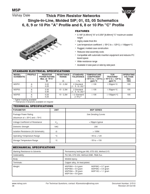
EXAMPLE: MSP08A-01-101G = A molded single-inline thick film resistor network with 8 pins on 0.100" [2.54mm] centers, 0.195" [4.95mm] maximum seated height, 01 Schematic, resistance value of 100 ohm and a tolerance of ± 2%.
STANDARD ELECTRICAL SPECIFICATIONS
MODEL/ SCHEMATIC PROFILE RESISTOR POWER RATING Max. @ 70°C* W 0.20 0.25 0.30 0.40 RESISTANCE RANGE STANDARD TOLERANCE ±% 2 Standard (1, 5, 10, 20)** 2 Standard (1, 5, 10, 20)** ± 2 Standard (± 5%)** TEMPERATURE TCR COEFFICIENT TRACKING* (- 55°C to + 125°C) (- 55°C to + 125°C) ppm/°C ppm/°C ± 100 ± 100 ± 100 ± 50ppm/°C ± 50ppm/°C ± 150ppm/°C OPERATING VOLTAGE Max. VDC 100 100 100
PARAMETER Package Power Rating (Maximum at + 25°C and + 70°C Voltage Coefficient of Resistance Dielectric Strength Isolation Resistance (03 Schematic) Operating Temperature Range Storage Temperature Range Veff VAC Ω °C °C < 50ppm typical 200 > 100M - 55 to + 125 - 55 to + 150 UNIT MSP SERIES See Derating Curves
GP1A05中文资料
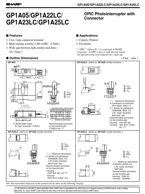
GP1A05/GP1A22LC/GP1A23LC/GP1A25LCOPIC Photointerrupter with Connectors Featuress Applicationss Outline Dimensions1. Uses 3-pin connector terminal2. High sensing accuracy (Slit width :0.5mm )3. Wide gap between light emitter and detec-*“OPIC ”(Optical IC ) is a trademark of SHARP and signal-processing circuit integrated onto a single chip.tor (5mm )Corporation.An OPIC consists of a light-detecting element gg Recommended connectors on the inserted side are show on the following 3rd page.(Unit :mm )1. Copiers, Printers2. Facsimiles-60504030201000.60.50.100.20.30.4Shield distance d (mm )-Detecting position d =3.5±0.3mmOutput LowOutput HighShield distance h (mm )Fig. 2 Low Level Output Voltage vs. Low Level Output CurrentFig. 1 Low Level Output Current vs.Ambient TemperatureL o w l e v l e o u t p u t v o l t a g e V O L (V )(2)(GP1A22LC /GP1A23LC /GP1A25LC :d =3.5±0.5mm )L o w l e v e l o u t p u t c u r r e n t I O L (m A )Detecting position h=3.0+2.0-1.5mms Precautions for Uses Recommended Connectors on the Inserted Side<<GP1A05>>q JAPAN AMP made El series connectorsHousing colorBlack Blue Green RedHousing Model No.172142-32-172142-34-172142-36-172142-38-172142-3Special terminalModel. No.(Material :Copper phosphide )AWG size Product shape Model No.AWG 26 to 22Bulk 170369-1Chain 170354-1AWG 30 to 26Bulk 170370-1Chain 170355-1(standard type )q JAPAN AMP made El series connectors (low profile type )q JAPAN AMP made El series connectors (amp mass termination )Housing colorBlack Blue Green RedHousing Model No.2-171822-34-171822-36-171822-38-171822-3Special terminalModel. No.AWG size ProductshapeMaterial Model No.AWG26 to 20Bulk Brass 170204-1Copperphosphide 170204-2Chain Brass 170262-1Copperphosphide170262-2AWG30 to 26Bulk Brass 170205-1Copperphosphide 170205-2Chain Brass 170263-1Copperphosphide170263-2Housing-terminal united type connector AWG28(Green )AWG26(Naturalcolor )AWG24(Black )AWG22(Red )172054-3172053-3172052-3172051-3* Terminal Material :Copper phosphide<<GP1A22LC/GP1A23LC >>een V CC and GND near the device in order to stabilize power supply line.However, do not perform the above cleaning using a soft cloth with cleaning solvent in the marking portion.In this case, use only the following type of cleaning solvent used for wiping off: Ethyl alcohol, Methyl alcohol, Isopropyl alcohol,When the cleaning solvents except for specified materials are used, please consult us.Housing Model No.H3P-SHF-AA S3P-SHF-1Special terminal Model. No.AWG sizeMaterialModel No.AWG sizeMaterialModel No.AWG26 to 22BrassSHF-001T-0.8SSAWG27 to 22BrassSHF-001T-0.8PCopperphosphide SHF-001T-0.8BS Copperphosphide-AWG30 to 26BrassSHF-002T-0.8SS AWG30 to 28BrassSHF-002T-0.8PCopperphosphide SHF-001T-0.8BS Copperphosphide-171822-3NaturalcolorNaturalcolorcase;therefore, dip cleaning or ultrasonic cleaning is prohibited.q JAPAN SOLDERLESS TERMINAL MSG. CO., LTD. made (Natural color •bulk )(1) It is recommended that a by-pass capacitor of more than 0.01µF be added betw (2) In this product, the PWB is fixed with a rear cover, and cleaning solvent may remain inside the (3) Remove dust or stains, using an air blower or a soft cloth moistened in cleaning solvent. (4) As for other general cautions, refer to the chapter “Precautions for Use .”Recommended connectors on the inserted side for GP1A05, G P1A22LC, and GP1A23LC a re shown below.。
2N3906中文资料(nte)中文数据手册「EasyDatasheet - 矽搜」
VCE = 1V, I C = 1mA
40 − − 80 − −
2N3905 2N3906
VCE = 1V, I C = 10mA
50 − 150 100 − 300
2N3905 2N3906
VCE = 1V, I C = 50mA
30 − − 60 − −
2N3905 2N3906
VCE = 1V, I C = 100mA
芯片中文手册,看全文,戳
2N3905 & 2N3906 硅PNP晶体管
一般用途
TO92类型封装
绝对最大额定值:
集电极 - 发射极电压,V
CEO . . . . . . . . . . . . . . . . . . . . . . . . . . . . . . . . . . . . . . . . . . . . . . . . . . . . . . 40V
器件总功耗(T
C = +255C), PD . . . . . . . . . . . . . . . . . . . . . . . . . . . . . . . . . . . . . . . . . . . . 1.5W
减免上述255℃. . . . . . . . . . . . . . . . . . . . . . . . . . . . . . . . . . . . . . . . . . . . . . . . . . . . . . 12MW / 5C
减免上述255℃. . . . . . . . . . . . . . . . . . . . . . . . . . . . . . . . . . . . . . . 5.0MW / 5C
器件总功耗(T
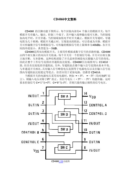
4066中文资料
Sine
Wave
5
VDD = 15V
Distortion
0
Frequency
VC = VDD = 5V, VSS = −5V RL = 10 kΩ,
0.
Response-Switch VIS = 5Vp-p, f= 1 kHz, (Figure 4)
1
“ON” (Frequency VC = VDD = 5V, VSS = −5V, RL = 1 kΩ,
当模拟开关的电源电压采用双电源时,例如 =﹢5V, =﹣5V(均对地0V 而 言),则输入电压对称于0V 的正、负信号电压(﹢5V~﹣5V)均能传输。这时 要求控制信号 C=“1”为+5V,C=“0”为-5V,否则只能传输正极性的信号电压。
CD4066引脚功能图
内部方框图
Absolute Maximum Ratings 绝对最大额定值:
5
=50pF(Figure 6)
0
RL=1.0kΩ, CL=50pF, (Figure 7)VOS(f) = ½ VOS(1.0 kHz)
6. VDD = 5.0V
0
8. VDD = 10V
0
8. VDD = 15V
5
Signal
Input
CIS Capacitance 信 号
8.
输入电容
0
Signal
20
80 240
320
0
Δ“ON”
RL = 10kΩ to (VDD − VSS/2) VCC = VDD, VIS = VSS to VDD
ΔRO Resistance
VDD = 10V
10
N Between Any 2
常用近500个三极管(MOSFET)中文资料

9011,9012,9013,9014,8050,8550三极管的区别9011 NPN 30V 30mA 400mW 150MHz 放大倍数20-809012 PNP 50V 500mA 600mW 低频管放大倍数30-909013 NPN 20V 625mA 500mW 低频管放大倍数40-1109014 NPN 45V 100mA 450mW 150MHz 放大倍数20-908050 NPN 25V 700mA 200mW 150MHz 放大倍数30-1008550 PNP 40V 1500mA 1000mW 200MHz 放大倍数40-140详情如下:90系列三极管参数90系列三极管大多是以90字为开头的,但也有以ST90、C或A90、S90、SS90、UTC90开头的,它们的特性及管脚排列都是一样的。
9011 结构:NPN集电极-发射极电压30V集电极-基电压50V射极-基极电压5V集电极电流0.03A耗散功率0.4W结温150℃特怔频率平均370MHZ放大倍数:D28-45 E39-60 F54-80 G72-108 H97-146 I132-1989012 结构:PNP集电极-发射极电压-30V集电极-基电压-40V射极-基极电压-5V集电极电流0.5A耗散功率0.625W结温150℃特怔频率最小150MHZ放大倍数:D64-91 E78-112 F96-135 G122-166 H144-220 I190-3009013 结构:NPN集电极-发射极电压25V集电极-基电压45V射极-基极电压5V集电极电流0.5A耗散功率0.625W结温150℃特怔频率最小150MHZ放大倍数:D64-91 E78-112 F96-135 G122-166 H144-220 I190-3009014 结构:NPN集电极-发射极电压45V集电极-基电压50V射极-基极电压5V集电极电流0.1A耗散功率0.4W结温150℃特怔频率最小150MHZ放大倍数:A60-150 B100-300 C200-600 D400-10009015 结构:PNP集电极-发射极电压-45V集电极-基电压-50V射极-基极电压-5V集电极电流0.1A耗散功率0.45W结温150℃特怔频率平均300MHZ放大倍数:A60-150 B100-300 C200-600 D400-10009016 结构:NPN集电极-发射极电压20V集电极-基电压30V射极-基极电压5V集电极电流0.025A耗散功率0.4W结温150℃特怔频率平均620MHZ放大倍数:D28-45 E39-60 F54-80 G72-108 H97-146 I132-1989018 结构:NPN集电极-发射极电压15V集电极-基电压30V射极-基极电压5V集电极电流0.05A耗散功率0.4W结温150℃特怔频率平均620MHZ放大倍数:D28-45 E39-60 F54-80 G72-108 H97-146 I132-198三极管85508550是一种常用的普通三极管。
DVPL0505S中文资料
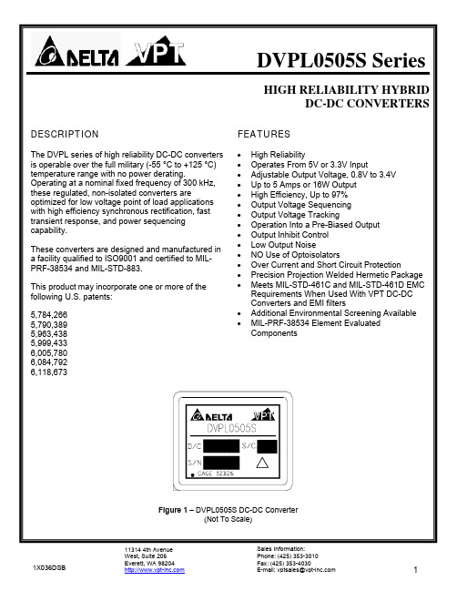
DVPL0505S Series
HIGH RELIABILITY HYBRID DC-DC CONVERTERS
DESCRIPTION
The DVPL series of high reliability DC-DC converters is operable over the full military (-55 °C to +125 °C) temperature range with no power derating. Operating at a nominal fixed frequency of 300 kHz, these regulated, non-isolated converters are optimized for low voltage point of load applications with high efficiency synchronous rectification, fast transient response, and power sequencing capability.
VOUT VOUT
VOUT VOUT VOUT
FAULT POWER DISSIPATION CAPACITIVE LOAD4
SWITCHING FREQUENCY
CASE ISOLATION
MTBF (MIL-HDBK-217F)
DYNAMIC
Load Step Output Transient5 Load Step Recovery2,5
3.3
3.30k
3.4
2.98k
R-TRIM
The output voltage is set with an external resistor connected from Trim pin to GND pin. This resistor must have a tolerance of 1% or less to achieve an accurate output voltage.
电子器件中文资料

下边资料的次序是纳米盘上的自动排列,请需要者自己看着找吧。
最后还有07年全年的《读者》E书下载,及几个小游戏。
4000系列数字集成电路资料大全.4000.rar/d/7d8425c10a0ff161c3e0e00037737a69c5d3980411432404AD620中文资料.pdf/d/b1961b23b272d8531b9f390fa570ae2c71c2d45024a6050074系列数字集成电路手册大全.pdf/d/b4c283d67d1af4aacf7b7c19d3d5aa3b71a8c58d7692c801速查速用世界可控硅代换手册.pdf/d/be70c47f9fc76db61c62e1caf90d0f4a87d1a68459699901最新集成电路应用300例.rar/d/365971ce99cae66629dd2d76d45b0307e83a21d461b83900怎样使用运算放大器.pdf/d/8ca6ba96b0a2d9d8ed0023ecde54908c909fb5cc8c8e2900新型实用电路制作200例.rar/d/b9f585eb5512f27c380fc3e01ce465e105592c00548f7d00新型电子电路应用实例精选.rar/d/2cd40d687adff1a0031927956c3ae4b16bd41b6489d48e00电子线路设计应用手册.rar/d/86601a2c9c3d346da2b7582806c525fc91e3cf55109a6301新编电子电路大全.rar/d/0ed4b1cba5ad94a5bdfabd410aae1c058c2bbd65aa8f6e00电子电路及电子器件.rar/d/0856a0265ffdc5947a7a4fe93ea34fa53539165b851ea700数字电路.rar/d/00fca0f91805c0f137bcfdc966caba0297c0e6d7dd4c3b00实用双向可控硅应用500例.rar/d/3ebb740d73718fb3cda67b20cb2d50620430f264cc2d6a00实用电子线路集.rar/d/4873ecc0445c91c3d7b444d6b71056bd6b45dc89ef6b8100实用电子电路大全.rar/d/2ca46fb365cedaee9451b79c697e8ff474d22aa6c5ebaf00实用单元电路及其应用.rar/d/3c77fff6e45fddf87dee1bf7788a1c242b1d1c4ef9119600三极管资料大全.rar/d/00de8710ba6c1e8c289ecaf61208d6b6ea32504677a90000绝对精品的硬件设计方面资料.rar/d/c8d1606af74af0a6f7a7f414376c7137e200fb588e460600简易可控硅整流电源电路.pdf/d/28430231e150b19c1d91d1a52f0104a8fef4b07eee510000电子电路大全(合订本).rar/d/7c041e86b457278bc289756622eca10562b31d68f6ba7a01电子电路集.pdf/d/cc133c04fb2ebe2abc1ed4b2a363046e6bff0d2bf8c04100电子电路百科全书(第五卷).rar/d/18148ed5200f99e6176c888024eb8e72d323fcf3e2007900电子电路.pdf/d/f1836309214f28fd8227efa0969e0d39c5261f29c88d4400电子爱好者实用电子制作.rar/d/05edad0c1b9b9c98eabc2847ca8a5d4cfa4fea48d9331f00常用电子元气件手册.pdf/d/f42c221af44585fee096c2b2c3f5d5da87591f3a7a143600常用电子元器件图片.pdf/d/90f6611e31ac9f60a761abb7af0ba31f50fb5a2a781f1c00常用稳压芯片篇.txt/d/6224bdf4fe9e168d36f3ef223422b6add262a8ed810c0000常用电子元器件简明手册.rar/d/00b9d1eedddd798047798152c65d916e257ff4e277702300常用电子元气件命名.pdf/d/3c89dc7fbb8fd14f64b93d946f16583a5c0c3848ce720800P8xC591_cn.pdf/d/8e6c43250690dc6baee98e3865798ee4fc85f5724ba14d00MAX485中文资料.pdf/d/15b701ca1ffd126726fdf070ea1f018d8344aa8bf19c0d00MAX280中文资料.pdf/d/12a35473a7bb0afbb25d41f079b2cbd5af770460877b0100MAX194中文资料.pdf/d/c4a65303e4422f2b661ee713c44e3000ab1ec8baf34b0100T8变压器.pdf/d/86d97d9ca03ec16cb94e885a63912561864f0dfb384d0200NE555.pdf/d/6eeb2db556192e988d3f45d6fc6a976d3743a54695d40300LM7805中文资料.pdf/d/20ade1675d2aebb22a5b7e8596cf421ad74fb6e0bc680400NE555中文资料.pdf/d/4437cbafdb450d9803022a7f145806736178b2647d8e0000MC1413.pdf/d/a8b41856cce7d8c13e68d7be0f7eba717d00bcc2be460100MCP3202中文资料.pdf/d/e6652d4504073a352f4a6e628575bcb68cd4b7bac3ed0b00MC3423.PDF/d/1856c527d115fecf23c7cc792b2df521f434795f4ad80100LM358中文资料.pdf/d/01055a8e69fd7f39469037ab678f9ed4a2807672378c0100LM339.rar/d/8c8b06f70cccad70c338f9f8bb9bf85745f5340af9480000lm2596.pdf/d/67de0105031f80ad657a9558635c3a8b38140cc53ada0c00LM2576中文资料.pdf/d/fc5567b2fa37f7ce88b5272536b2d817eb231c50971e0400lm1117中文资料.pdf/d/f24586db9afc12e7f9bf32371f24b389452a1cc4a7bb0b00LM393中文资料.pdf/d/1961b1559934b7bf617ae57027e87ebb7d12aea50a9a0300LM363中文资料.pdf/d/7e83da8b44365c274829b181ecf725a2291407804cb40100LM7909中文资料.pdf/d/8ce4617cb1123fda1ad10ad38d4493a6480e86f5d4bf0000LMD18200.doc/d/a7e301b93175eb71345299272395fce9e06a30a8009c0100lm324中文资料.pdf/d/cc590a103a433200fdfb3a57f44f5f383d2ee0b4557d0a00LM317中文资料.pdf/d/686a9606b1dd1cca239d8a6bcc8e27d4b45c1f8c24d50d00lm211lm311中文资料.pdf/d/eb9f6ebac497c099445f95a4ad95a0a44730341a715d0b00LM140.pdf/d/3876aea02373e492cdb7da633c9ba26d5f250e06d8e10200LM358.pdf/d/7816ffab592a9e37d9c493dd238fc6b6e55397be8e5e0100LM109.pdf/d/a70eaf6138bb71be74d0431224cbd5d0c7f1136a55740100lm3s317_ds_cn.pdf/d/bd34bf2a2ab69f935911e60206bd5e1a67e6f06ca0215d00 LF398中文资料.pdf/d/bcd8edd55f76babe047e7e1e8e61045af8129ab1866e0100L290-L291-L292.pdf/d/2e0ab9638f84016c18a6ff0fc817b8dbf1043857e30b0400ICL7135中文资料.pdf/d/71e1b23dbc5dff6f6fef9c002be6420f5968745750710800ICL7104中文资料.pdf/d/e07abec1e557ad53c159d7156237bfa86e842cb549820100fm3135_ds.pdf/d/fc97032bc0142c568bdd39f8140d82c6ae4ee9b175260400cd40161中文资料pdf.pdf/d/40230b71ccbbc78b9355e8946d1e4391efecf2199da10200最新世界三极管特性代换手册.r/d/6605148cde3dddb2a4bb9123eb0dcdb6721a053f286c7601lm3s310_ds_cn.pdf/d/bb01eb82cbddbc6fabae95b5a3f631f1d32d3331750e5700cmos4000器件中文资料.pdf/d/bde8cef1903e5f776ddae591fe4b9fe4dd41fa2023074800cd40109中文资料pdf.pdf/d/202883c137a9443ae5aad82ac01c0c5d5b027bfceeb50100cd40105中文资料pdf.pdf/d/b56e06f4a9b172b10908429505b829f1b06b46934bca0100ds1302中文资料.pdf/d/8ffe86b97d76a8cc3fffe2b8b7d7d411ea84ad0bac730300cd40163中文资料pdf.pdf/d/305f9eca8225b8333aafa3a1bd0c4c3c1c3ac34338a10200cd40147中文资料pdf.pdf/d/e3380153eb1198bc857e579999fc3dddb55b460294f20100cd4076中文资料.pdf/d/d000f62e7c0c80c37332f73d5a9200afa8a7f4b572f30200cd4071中文资料.pdf/d/49f8cce83e6ab3e4d593fa45e1f0e685dcbb5186db3a0200cd4070中文资料.pdf/d/82edf36cc8617e3356612ac573e356ba89959470a3420200cd4068中文资料.pdf/d/18c87ad5f8690c9cd1a33121bfd1ba3040256c7d8f490200cd4067中文资料.pdf/d/e6966eea3a191a3186dd7bfb5f19f031b430ea7121530200cd4055中文资料.pdf/d/33d92d1285e92130dbb263df34bebe04f1418d98e29f0300cd4038中文资料.pdf/d/bebc590afbebe766436886d23fbc5205344cbe07d5690300cd4029中文资料pdf.pdf/d/0d4dc7d75ded5885fd3e475e8071f438921d796cbd750400cd4048中文资料.pdf/d/846d38f344ce9ef88598d6e69a542300fed3c3d7d33f0200cd4047中文资料.pdf/d/36a5eec356ffc0baf497d07e71f28081732d28bc145e0200cd4035中文资料.pdf/d/c7b4075b5bda2910cbfdc61bd13730a2d7ab41f161a10300cd4034中文资料.pdf/d/b6dadf2ee2883540208c0f0e06d930fbbf0812016faf0400cd4028中文资料pdf.pdf/d/557cd672fe94a58e1e0c7b508bd095c74c7851d7fb820300cd4024中文资料pdf.pdf/d/c2196481f081938dbb92ed67395098e681fac3206cf10300cd4027中文资料pdf.pdf/d/348e802290198d2503df1013653fd744b97ccdba31ef0200 AT89S51.pdf/d/dccdecb6e6192d5581e790a27bf787eb9a354e1335350900cd4053.pdf/d/404342f322a3a932c98775f207d3ebfd4086551dacb10200cd4034中文资料.pdf/d/49106b6ade07c448f2e9f0d4c232dd8f818961bf6faf0400cd4028中文资料pdf.pdf/d/21e60f5ad93242cad1720458dce6b23333765ec7fb820300cd4027中文资料pdf.pdf/d/60d154cb4a834783bdc59afd3385cd025*********ef0200cd4022中文资料pdf.pdf/d/1057c76c8deff8300c6a6db430ba3282d53d9dbfc70d0400att7021cn.pdf/d/0e5d65285c35682e713bddf0a405e0326a64aba2c6c20a00BA5101BA5201.pdf/d/5d16c3c4e4ac5e156c4241ea590dba00ef7246403acf0400AT89S51.pdf/d/237f01593ba5bddc8665e29116ff139e19c340d435350900AT89LV52.pdf/d/5879e4ac095f60ca5e2b92beb242eaac1c5665cedf300800ad9850中文资料.pdf/d/38a283d55c2c6ceb04694c7a5534c3ae16ab96a6dc6e1c00AT89C1051U.pdf/d/559f6cf5bc2aefa3bbaf4bc6d6f9dd17042dcba1f8d40400 AD673.pdf/d/559f6cf5bc2aefa3bbaf4bc6d6f9dd17042dcba1f8d40400AD620中文资料.pdf/d/145656a8efc258c014c5330ed03482a33a04ea6524a60500AD594_595.pdf/d/6028f9ccfdf02af289e312c94ef8cfc0d9275efdb6220200AD346中文资料.pdf/d/7bd0a4417a8213a7dc982986fbcdae8ce53d9e53fa4401009013.pdf/d/9057c57766e0d1fded4e6a49804e23949c2177bc6d9501008050.pdf/d/24e3b9655ebf0b2f019abd07baaa995fa98f45bf31a1020078xx.pdf/d/af10e44a0a8b804bdd6336b88e2188cf195375644b1c010074LS164中文资料.pdf/d/201383c7b23d7057d102cfc148946d045797b4a88914030074ls245中文资料.pdf/d/37f26e3d5349c02dc216bdc7a487060d1332e94f7501030074LS138中文资料.pdf/d/52f4c8c7b39181704008ceb6e89ea8095faaab98cbbe030074ls138.PDF/d/7aa7e214ce5dfe4c5dce8d9c78ab396289ca517377b9030074ls74.PDF/d/9e1051ab95e509fe3414830be349e6d7d6f56374297a060074ls04.PDF/d/e8a4bad83b00a61a514f295ef7d36aa064801b744472040074LS14中文资料.pdf/d/8938dbc43cdb1a232112a8f69e0b0f7e50357cb54389030074HC245中文资料.pdf/d/d045498e1b5a8b831fb554e3059f7c9c6a3ed92d1701030024c02中文官方资料手册pdf.pdf/d/5463179db3bbb8a494d38f0ab48c8cbb9cf6aece299c090074ALS245.pdf/d/b4c462102ac87887e8e5059e001f16647c213459b13f01004N25中文资料.pdf/d/c818ecf73638d05fb5489690e28b91c94c0976af7ccb0100USB DISK EJECT.EXE/d/4102ee837c5b11d7d7e3d40c759bd5b384154f33007c0d00TEA1062.pdf/d/569c7b2bf61ebf2e2c01d7fcb3bdb0a3f1b83a0d8b4e030078xx.pdf/d/dc3547b7951a28c30c447002adfc743b2cd8174a4b1c010074ls245中文资料.pdf/d/f0fd2d9a704cfc09571d7f694b8e5625ea2577f57501030074LS138中文资料.pdf/d/8df689b9e0e1157387ae34ffb186587654607dc5cbbe030074ls138.PDF/d/906f5068200722722dd009f2c0558d2ca954855d77b9030074ls74.PDF/d/d4ce35981359c38e4e10a143913dbc77ec41b17c297a060074LS14中文资料.pdf/d/500d0dd2c24ca57fdd5f81887ce014ee383cf15f4389030074ls04.PDF/d/00b330534fc4824625e3f5aadb970e2cb07c17204472040024c02中文官方资料手册pdf.pdf/d/0dfded751578a730e85acec4fecb3ff3ecb3e344299c090074HC245中文资料.pdf/d/ff5c91227f1bf663c1326fc19d5295f02035768b1701030074ALS245.pdf/d/0347de88ba42c7981ec9d8cb0829ed27dee125a8b13f01001N4148smd.pdf/d/885391bb8724b237c52840be7996214047193380cfa008002n4403.PDF/d/20bc155264d25b57a981c63afab4b0be6bb806f2b4f700002n4401.PDF/d/40c749e3a06284cca55f4964a1322308e344b26651f70000LMD18200.doc/d/58c3a544b3cc4481889d5c85b54087756849a92e009c0100。
MAX6709-MAX6714资料
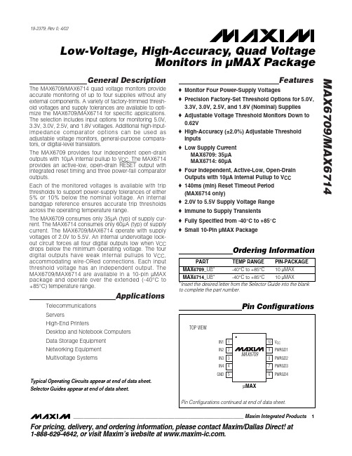
General DescriptionThe MAX6709/MAX6714 quad voltage monitors provide accurate monitoring of up to four supplies without any external components. A variety of factory-trimmed thresh-old voltages and supply tolerances are available to opti-mize the MAX6709/MAX6714 for specific applications.The selection includes input options for monitoring 5.0V,3.3V, 3.0V, 2.5V, and 1.8V voltages. Additional high-input-impedance comparator options can be used as adjustable voltage monitors, general-purpose compara-tors, or digital-level translators.The MAX6709 provides four independent open-drain outputs with 10µA internal pullup to V CC . The MAX6714provides an active-low, open-drain RESET output with integrated reset timing and three power-fail comparator outputs.Each of the monitored voltages is available with trip thresholds to support power-supply tolerances of either 5% or 10% below the nominal voltage. An internal bandgap reference ensures accurate trip thresholds across the operating temperature range.The MAX6709 consumes only 35µA (typ) of supply cur-rent. The MAX6714 consumes only 60µA (typ) of supply current. The MAX6709/MAX6714 operate with supply voltages of 2.0V to 5.5V. An internal undervoltage lock-out circuit forces all four digital outputs low when V CC drops below the minimum operating voltage. The four digital outputs have weak internal pullups to V CC ,accommodating wire-ORed connections. Each input threshold voltage has an independent output. The MAX6709/MAX6714 are available in a 10-pin µMAX package and operate over the extended (-40°C to +85°C) temperature range.ApplicationsTelecommunications ServersHigh-End PrintersDesktop and Notebook Computers Data Storage Equipment Networking Equipment Multivoltage SystemsFeatureso Monitor Four Power-Supply Voltageso Precision Factory-Set Threshold Options for 5.0V,3.3V, 3.0V, 2.5V, and 1.8V (Nominal) Supplies o Adjustable Voltage Threshold Monitors Down to 0.62V o High-Accuracy (±2.0%) Adjustable Threshold Inputs o Low Supply CurrentMAX6709: 35µA MAX6714: 60µAo Four Independent, Active-Low, Open-Drain Outputs with 10µA Internal Pullup to V CC o 140ms (min) Reset Timeout Period (MAX6714 only)o 2.0V to 5.5V Supply Voltage Range o Immune to Supply Transients o Fully Specified from -40°C to +85°C o Small 10-Pin µMAX PackageMAX6709/MAX6714Low-Voltage, High-Accuracy, Quad VoltageMonitors in µMAX Package________________________________________________________________Maxim Integrated Products 1Ordering InformationPin Configurations19-2379; Rev 0; 4/02For pricing, delivery, and ordering information,please contact Maxim/Dallas Direct!at 1-888-629-4642, or visit Maxim’s website at .Typical Operating Circuits appear at end of data sheet.Selector Guides appear at end of data sheet.to complete the part number.M A X 6709/M A X 6714Low-Voltage, High-Accuracy, Quad Voltage Monitors in µMAX Package 2_______________________________________________________________________________________ABSOLUTE MAXIMUM RATINGSELECTRICAL CHARACTERISTICS (MAX6709)Stresses beyond those listed under “Absolute Maximum Ratings” may cause permanent damage to the device. These are stress ratings only, and functional operation of the device at these or any other conditions beyond those indicated in the operational sections of the specifications is not implied. Exposure to absolute maximum rating conditions for extended periods may affect device reliability.All Pins to GND.........................................................-0.3V to +6V Input/Output Current (all pins)............................................20mA Continuous Power Dissipation (T A = +70°C)10-Pin µMAX (derate 5.6mW/°C above +70°C)..........444mWOperating Temperature Range ...........................-40°C to +85°C Storage Temperature Range.............................-65°C to +150°C Junction Temperature......................................................+150°C Lead Temperature (soldering, 10s).................................+300°CMAX6709/MAX6714Low-Voltage, High-Accuracy Quad, VoltageMonitors in µMAX Package_______________________________________________________________________________________3ELECTRICAL CHARACTERISTICS (MAX6714)Note 2:Condition at V CC = 1V is guaranteed only from T A = 0°C to +70°C.Note 3:Monitored voltage 5V/3.3V is also the device supply. In the typical condition, supply current splits as follows: 25µA for theresistor-divider, and the rest for other circuitry.M A X 6709/M A X 6714Low-Voltage, High-Accuracy, Quad Voltage Monitors in µMAX Package 4_______________________________________________________________________________________Typical Operating Characteristics(V CC = 5V, T A = +25°C, unless otherwise noted.)SUPPLY CURRENTvs. SUPPLY VOLTAGE (MAX6709)SUPPLY VOLTAGE (V)S U P P L Y C U R R E N T (µA )5.04.53.5 4.01.0 1.5 2.0 2.5 3.00.5510152025303540455000 5.5SUPPLY CURRENTvs. SUPPLY VOLTAGE (MAX6714)SUPPLY VOLTAGE (V)S U P P L Y C U R R E N T (µA )5.04.53.5 4.01.0 1.5 2.0 2.5 3.00.510203040506070809010005.5NORMALIZED THRESHOLD ERROR vs. SUPPLY VOLTAGE (MAX6709)SUPPLY VOLTAGE (V)N O R M A L I Z E D T H R E S H O L D E R R O R (%)5.04.53.54.03.02.5-0.0100.010.020.030.040.050.060.070.08-0.022.05.5NORMALIZED THRESHOLD vs. TEMPERATURE (MAX6709)M A X 6709/14 t o c 04TEMPERATURE (°C)N O R M A L I Z E D T H R E S H OL D6035-1510-0.15-0.10-0.0500.050.100.150.20-0.20-4085NORMALIZED PFI_ THRESHOLD vs. TEMPERATURE (MAX6714)TEMPERATURE (°C)N O R M A L I Z E D P F I _ T H R E S H O L D603510-150.9920.9940.9960.9981.0001.0021.0041.0061.0081.0100.990-4085OUTPUT VOLTAGE LOW vs. SINK CURRENTSINK CURRENT (mA)O U T P U T V O L T A G E L O W (m V )98672345120406080100120140160180200010MAXIMUM TRANSIENT DURATION vs. V CC OVERDRIVE (MAX6714)V CC OVERDRIVE (mV)M A X I M U M T R A N S I E N T D U R A T I O N (µs )90080060070020030040050010010203040506070809010011012001000MAXIMUM TRANSIENT DURATION vs. PFI_ OVERDRIVE (MAX6714)PFI_ OVERDRIVE (mV)M A X I M U M T R A N S I E N T D U R A T I O N (µs )500100402010203040506070809010011012001000RESET TIMEOUT PERIOD vs. TEMPERATURE (MAX6714)M A X 6709/14 t o c 09TEMPERATURE (°C)R E S E T T I M E O U T P E R I O D (m s )603510-15211212213214215216210-4085MAX6709/MAX6714Low-Voltage, High-Accuracy Quad, VoltageMonitors in µMAX Package_______________________________________________________________________________________5Typical Operating Characteristics (continued)(V CC = 5V, T A = +25°C, unless otherwise noted.)PROPAGATION DELAY (WITH 100mV OVERDRIVE)MAX6709/14 toc1010µs/div PWRGD_ (PFO_)2V/div IN_ (PFI_)100mV/div AC-COUPLED PFO_ PULLUP AND PULLDOWN RESPONSE(C _ = 47pF)MAX6709/14 toc1110µs/divPFO_2V/divPFI_50mV/div AC-COUPLEDRESET TIMEOUT DELAYMAX6709/14 toc1240ms/divRESET 2V/divMR 2V/divM A X 6709/M A X 6714Low-Voltage, High-Accuracy, Quad Voltage Monitors in µMAX Package 6_______________________________________________________________________________________Detailed DescriptionThe MAX6709/MAX6714 are low-power, quad voltage monitors designed for multivoltage systems. Preset voltage options for 5.0V, 3.3V, 3.0V, 2.5V, and 1.8V make these quad monitors ideal for applications such as telecommunications, desktop and notebook comput-ers, high-end printers, data storage equipment, and networking equipment.The MAX6709/MAX6714 have an internally trimmed threshold that minimizes or eliminates the need for external components. The four open-drain outputs have weak (10µA) internal pullups to V CC , allowing them to interface easily with other logic devices. The weak inter-nal pullups can be overdriven by external pullups to any voltage from 0 to 5.5V. Internal circuitry prevents currentflow from the external pullup voltage to V CC . The out-puts can be wire-ORed for a single power-good signal.The MAX6709 quad voltage monitor includes an accu-rate reference, four precision comparators, and a series of internally trimmed resistor-divider networks to set the factory-fixed threshold options. The resistor net-works scale the specified IN_ reset voltages to match the internal reference/comparator voltage. Adjustable threshold options bypass the internal resistor networks and connect directly to one of the comparator inputs (an external resistor-divider network is required for threshold matching). The MAX6709 monitors power supplies with either 5% or 10% tolerance specifica-tions, depending on the selected version. Additional high-input-impedance comparator options can be usedMAX6709/MAX6714Low-Voltage, High-Accuracy Quad, VoltageMonitors in µMAX Package_______________________________________________________________________________________7Figure 1. MAX6709 Functional DiagramM A X 6709/M A X 6714as an adjustable voltage monitor, general-purpose comparator, or digital-level translator.The MAX6714 quad voltage monitor/reset offers one fixed input with internal timing for µP reset, three power-fail comparators, and a manual reset input (MR ). RESET asserts low when V CC drops below its threshold or MR is driven low. Each of the three power-fail inputs connects directly to one of the comparator inputs.When any input is higher than the threshold level, the output is high. The output goes low as the input drops below the threshold voltage. The undervoltage lockout circuitry remains active and all outputs remain low with V CC down to 1V (Figures 1 and 2).Applications InformationHysteresisWhen the voltage on one comparator input is at or near the voltage on another input, ambient noise generally causes the comparator output to oscillate. The most common way to eliminate this problem is through hys-teresis. When the two comparator input voltages are equal, hysteresis causes one comparator input voltage to move quickly past the other, thus taking the input out of the region where oscillation occurs. Standard com-parators require hysteresis to be added through the use of external resistors. The external resistive network usually provides a positive feedback to the input in order to cause a jump in the threshold voltage when output toggles in one direction or the other. TheseLow-Voltage, High-Accuracy, Quad Voltage Monitors in µMAX Package 8_______________________________________________________________________________________resistors are not required when using the MAX6709/MAX6714 because hysteresis is built into the device.MAX6709/MAX6714 hysteresis is typically 0.3% of the threshold voltage.Undervoltage Detection CircuitThe open-drain outputs of the MAX6709/MAX6714 can be configured to detect an undervoltage condition.Figure 3 shows a configuration where an LED turns on when the comparator output is low, indicating an undervoltage condition.The MAX6709/MAX6714 can also be used in applica-tions such as system supervisory monitoring, multivolt-age level detection, and V CC bar graph monitoring (Figure 4).Window DetectionA window detector circuit uses two auxiliary inputs in a configuration such as the one shown in Figure 5.External resistors R1–R4 set the two threshold voltages (V TH1and V TH4) of the window detector circuit. Window width (∆V TH ) is the difference between the threshold voltages (Figure 6).Adjustable InputThe MAX6709 offers several monitor options with adjustable reset thresholds. The MAX6714 has three monitored inputs with adjustable thresholds. The thresh-old voltage at each adjustable IN_ (PFI_) input is typically 0.62V. To monitor a voltage >0.62V, connect a resistor-divider network to the circuit as shown in Figure 7.V INTH = 0.62V ✕(R1 + R2) / R2MAX6709/MAX6714Low-Voltage, High-Accuracy Quad, VoltageMonitors in µMAX Package_______________________________________________________________________________________9Figure 3. Quad Undervoltage Detector with LED IndicatorsCCFigure 5. Window Detection Figure 6. Output Response of Window Detector CircuitM A X 6709/M A X 6714Or, solved in terms of R1:R1 = R2 ((V INTH / 0.62V) - 1)Unused InputsThe unused inputs (except the adjustable) are internally connected to ground through the lower resistors of the threshold-setting resistor pairs. The adjustable input,however, must be connected to ground if unused.Reset OutputThe MAX6714 RESET output asserts low when V CC drops below its specified threshold or MR asserts low and remains low for the reset timeout period (140ms min) after V CC exceeds its threshold and MR deasserts (Figure 8). The output is open drain with a weak (10µA)internal pullup to V CC . For many applications, no exter-nal pullup resistor is required to interface with other logic devices. An external pullup resistor to any voltage from 0 to 5.5V overdrives the internal pullup if interfac-ing to different logic supply voltages (Figure 9). Internal circuitry prevents reverse current flow from the external pullup voltage to V CC .Manual Reset InputMany µP-based products require manual reset capabili-ty, allowing the operator, a test technician, or external logic circuitry to initiate a reset. A logic low on MR asserts RESET low. RESET remains asserted while MR is low, and during the reset timeout period (140ms min)after MR returns high. The MR input has an internal 20k Ωpullup resistor to V CC , so it can be left open if unused.Drive MR with TTL or CMOS-logic levels, or with open-drain/collector outputs. Connect a normally open momen-tary switch from MR to GND to create a manual reset function; external debounce circuitry is not required. If MR is driven from long cables or if the device is used in anoisy environment, connecting a 0.1µF capacitor from MR to GND provides additional noise immunity.Reseting the µP from a 2nd Voltage(MAX6714)The MAX6714 can be configured to assert a reset from a second voltage by connecting the power-fail output to manual reset. As the V PFI_falls below its threshold, PFO goes low and asserts the reset output for the reset time-out period after the manual reset input is deasserted.(See Typical Operating Circuit.)Power-Supply Bypassing and GroundingThe MAX6709/MAX6714 operate from a single 2.0V to 5.5V supply. In noisy applications, bypass V CC with a 0.1µF capacitor as close to V CC as possible.Low-Voltage, High-Accuracy, Quad Voltage Monitors in µMAX Package 10______________________________________________________________________________________Figure 8. RESET Output Timing DiagramMAX6709/MAX6714Low-Voltage, High-Accuracy Quad, VoltageMonitors in µMAX Package______________________________________________________________________________________11Pin Configurations (continued)Chip InformationTRANSISTOR COUNT: 1029PROCESS: BiCMOSM A X 6709/M A X 6714Low-Voltage, High-Accuracy, Quad Voltage Monitors in µMAX Package 12______________________________________________________________________________________MAX6709/MAX6714Low-Voltage, High-Accuracy, Quad VoltageMonitors in µMAX PackageMaxim cannot assume responsibility for use of any circuitry other than circuitry entirely embodied in a Maxim product. No circuit patent licenses are implied. Maxim reserves the right to change the circuitry and specifications without notice at any time.Maxim Integrated Products, 120 San Gabriel Drive, Sunnyvale, CA 94086 408-737-7600 ____________________13©2002 Maxim Integrated ProductsPrinted USAis a registered trademark of Maxim Integrated Products.Package Information(The package drawing(s) in this data sheet may not reflect the most current specifications. For the latest package outline information,go to /packages .)。