PMEG4030EP,115;中文规格书,Datasheet资料
肖特基PMEG4030ER

3 A low VF MEGA Schottky barrier rectifier
Rev. 01 — 11 August 2009
Product data sheet
1. Product profile
1.1 General description
Planar Maximum Efficiency General Application (MEGA) Schottky barrier rectifier with an integrated guard ring for stress protection, encapsulated in a SOD123W small and flat lead Surface-Mounted Device (SMD) plastic package.
total power dissipation
Tamb ≤ 40 °C Tsp ≤ 130 °C square wave; tp = 8 ms Tamb ≤ 25 °C
[1] -
[2] -
[3][4] [3][5] -
[3][1] -
Max Unit
40
V
3
A
3
A
50
A
0.57 W
0.95 W
1.8
W
PMEG4030ER_1
Product data sheet
Rev. 01 — 11 August 2009
© NXP B.V. 2009. All rights reserved.
2 of 13
NXP Semiconductors
PMEG4030ER
3 A low VF MEGA Schottky barrier rectifier
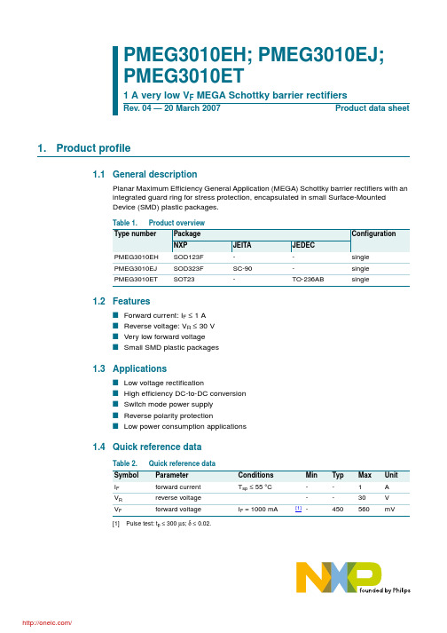
PMEG3010EJ,115;PMEG3010EH,115;中文规格书,Datasheet资料
Marking code[1] AA AK *AV
PMEG3010EH_EJ_ET_4
Product data sheet
/
Rev. 04 — 20 March 2007
© NXP B.V. 2007. All rights reserved.
2 of 11
NXP Semiconductors
Conditions in free air
PMEG3010EJ
PMEG301esistance from junction to solder point
PMEG3010EH PMEG3010EJ PMEG3010ET
Min Typ Max Unit
[1]
Rev. 04 — 20 March 2007
© NXP B.V. 2007. All rights reserved.
4 of 11
NXP Semiconductors
PMEG3010EH/EJ/ET
1 A very low VF MEGA Schottky barrier rectifiers
103 IF (mA)
3. Ordering information
Simplified outline Symbol
[1]
1
2
001aab540
1
2
sym001
3
1
2
3
1
2 n.c.
006aaa436
Table 4. Ordering information
Type number Package
Name
Description
[4] Soldering point of cathode tab.
PMEG3020EH中文资料

6. Thermal characteristics
Table 7: Thermal characteristics
Fig 2. Reverse current as a function of reverse voltage; typical values
9397 750 15077
Product data sheet
Rev. 03 — 31 May 2005
© Koninklijke Philips Electronics N.V. 2005. All rights reserved.
9397 750 15077
Product data sheet
Rev. 03 — 31 May 2005
© Koninklijke Philips Electronics N.V. 2005. All rights reserved.
2 of 9
Philips Semiconductors
PMEG3020EH; PMEG3020EJ
1.4 Quick reference data
Table 2: Symbol IF VR VF
Quick reference data
Parameter
Conditions
forward current
Tsp ≤ 55 °C
reverse voltage
forward voltage
IF = 2000 mA
Symbol Parameter
PMEG4010CEA 40V 1A MEGA 氧化铬栅栏电阻说明书

PMEG4010CEA40 V, 1 A low VF MEGA Schottky barrier rectifier18 November 2016Product data sheet1. General descriptionPlanar Maximum Efficiency General Application (MEGA) Schottky barrier rectifier with anintegrated guard ring for stress protection, encapsulated in a very small SOD323 (SC-76) Surface-Mounted Device (SMD) plastic package.2. Features and benefits•Average forward current: I F(AV) ≤ 1 A•Reverse voltage: V R ≤ 40 V•Low forward voltage typ. V F = 720 mV•Low reverse current typ. I R = 1.5 µA•Very small SMD plastic package•AEC-Q101 qualified3. Applications•Low voltage rectification•High efficiency DC-to-DC conversion•Switch mode power supply•Reverse polarity protection•Low power consumption applications•Automotive applications4. Quick reference data[1]Very short test pulse to keep junction temperature unchanged.5. Pinning information6. Ordering information7. Marking8. Limiting valuesTable 5. Limiting values[1]Device mounted on an FR4 PCB, single-sided copper, tin-plated and standard footprint.[2]Device mounted on an FR4 PCB, single-sided copper, tin-plated, mounting pad for cathode 1 cm2.9. Thermal characteristics[1]For Schottky barrier diodes thermal runaway has to be considered, as in some applications the reverse power losses P R are asignificant part of the total power losses.[2]Device mounted on an FR4 PCB, single-sided copper, tin-plated and standard footprint.[3]Device mounted on an FR4 PCB, single-sided copper, tin-plated, mounting pad for cathode 1 cm2.[4]Soldering point of cathode tab.10. Characteristics[1]Very short test pulse to keep junction temperature unchanged.11. Test informationThe current ratings for the typical waveforms are calculated according to the equations: I F(AV) = I M× δ with I M defined as peak current, I RMS = I F(AV) at DC, and I RMS = I M × √δ with I RMS defined asRMS current.Quality informationThis product has been qualified in accordance with the Automotive Electronics Council (AEC)standard Q101 - Stress test qualification for discrete semiconductors, and is suitable for use inautomotive applications.12. Package outline13. Soldering14. Revision history15. Legal informationData sheet status[1]Please consult the most recently issued document before initiating orcompleting a design.[2]The term 'short data sheet' is explained in section "Definitions".[3]The product status of device(s) described in this document may havechanged since this document was published and may differ in case of multiple devices. The latest product status information is available on the Internet at URL .DefinitionsPreview — The document is a preview version only. The document is still subject to formal approval, which may result in modifications or additions. Nexperia does not give any representations or warranties as tothe accuracy or completeness of information included herein and shall have no liability for the consequences of use of such information.Draft — The document is a draft version only. The content is still under internal review and subject to formal approval, which may result in modifications or additions. Nexperia does not give anyrepresentations or warranties as to the accuracy or completeness of information included herein and shall have no liability for the consequences of use of such information.Short data sheet — A short data sheet is an extract from a full data sheet with the same product type number(s) and title. A short data sheet is intended for quick reference only and should not be relied upon to contain detailed and full information. For detailed and full information see the relevant full data sheet, which is available on request via the local Nexperia sales office. In case of any inconsistency or conflict with theshort data sheet, the full data sheet shall prevail.Product specification — The information and data provided in a Product data sheet shall define the specification of the product as agreed between Nexperia and its customer, unless Nexperia andcustomer have explicitly agreed otherwise in writing. In no event however, shall an agreement be valid in which the Nexperia productis deemed to offer functions and qualities beyond those described in the Product data sheet.DisclaimersLimited warranty and liability — Information in this document is believed to be accurate and reliable. However, Nexperia does not giveany representations or warranties, expressed or implied, as to the accuracy or completeness of such information and shall have no liability for the consequences of use of such information. Nexperia takes no responsibility for the content in this document if provided by an information source outside of Nexperia.In no event shall Nexperia be liable for any indirect, incidental,punitive, special or consequential damages (including - without limitation -lost profits, lost savings, business interruption, costs related to the removal or replacement of any products or rework charges) whether or not such damages are based on tort (including negligence), warranty, breach of contract or any other legal theory.Notwithstanding any damages that customer might incur for any reason whatsoever, Nexperia’s aggregate and cumulative liability towards customer for the products described herein shall be limited in accordance with the Terms and conditions of commercial sale of Nexperia.Right to make changes — Nexperia reserves the right tomake changes to information published in this document, including without limitation specifications and product descriptions, at any time and without notice. This document supersedes and replaces all information supplied prior to the publication hereof.Suitability for use in automotive applications — This Nexperiaproduct has been qualified for use in automotiveapplications. Unless otherwise agreed in writing, the product is not designed, authorized or warranted to be suitable for use in life support, life-critical or safety-critical systems or equipment, nor in applications where failure or malfunction of a Nexperia product can reasonably be expectedto result in personal injury, death or severe property or environmental damage. Nexperia and its suppliers accept no liability forinclusion and/or use of Nexperia products in such equipment or applications and therefore such inclusion and/or use is at the customer's own risk.Quick reference data — The Quick reference data is an extract of the product data given in the Limiting values and Characteristics sections of this document, and as such is not complete, exhaustive or legally binding. Applications — Applications that are described herein for any of these products are for illustrative purposes only. Nexperia makesno representation or warranty that such applications will be suitable for the specified use without further testing or modification.Customers are responsible for the design and operation of their applications and products using Nexperia products, and Nexperiaaccepts no liability for any assistance with applications orcustomer product design. It is customer’s sole responsibility to determine whether the Nexperia product is suitable and fit for thecustomer’s applications and products planned, as well as for the planned application and use of customer’s third party customer(s). Customers should provide appropriate design and operating safeguards to minimize the risks associated with their applications and products.Nexperia does not accept any liability related to any default,damage, costs or problem which is based on any weakness or defaultin the customer’s applications or products, or the application or use by customer’s third party customer(s). Customer is responsible for doing all necessary testing for the customer’s applications and products using Nexperia products in order to avoid a default of the applicationsand the products or of the application or use by customer’s third party customer(s). Nexperia does not accept any liability in this respect.Limiting values — Stress above one or more limiting values (as defined in the Absolute Maximum Ratings System of IEC 60134) will cause permanent damage to the device. Limiting values are stress ratings only and (proper) operation of the device at these or any other conditions above thosegiven in the Recommended operating conditions section (if present) or the Characteristics sections of this document is not warranted. Constant or repeated exposure to limiting values will permanently and irreversibly affect the quality and reliability of the device.Terms and conditions of commercial sale — Nexperiaproducts are sold subject to the general terms and conditions of commercial sale, as published at /profile/terms, unless otherwise agreed in a valid written individual agreement. In case an individual agreement is concluded only the terms and conditions of the respective agreement shall apply. Nexperia hereby expressly objects toapplying the customer’s general terms and conditions with regard to the purchase of Nexperia products by customer.No offer to sell or license — Nothing in this document may be interpretedor construed as an offer to sell products that is open for acceptance or the grant, conveyance or implication of any license under any copyrights, patents or other industrial or intellectual property rights.Export control — This document as well as the item(s) described herein may be subject to export control regulations. Export might require a prior authorization from competent authorities.Translations — A non-English (translated) version of a document is for reference only. The English version shall prevail in case of any discrepancy between the translated and English versions.TrademarksNotice: All referenced brands, product names, service names and trademarks are the property of their respective owners.16. Contents1. General description (1)2. Features and benefits (1)3. Applications (1)4. Quick reference data (1)5. Pinning information (2)6. Ordering information (2)7. Marking (2)8. Limiting values (3)9. Thermal characteristics (3)10. Characteristics (5)11. Test information (8)12. Package outline (9)13. Soldering (9)14. Revision history (11)15. Legal information (12)For more information, please visit: Forsalesofficeaddresses,pleasesendanemailto:*************************** Date of release:18 November 2016Mouser ElectronicsAuthorized DistributorClick to View Pricing, Inventory, Delivery & Lifecycle Information:N experia:PMEG4010CEAX。
PMEG6010CEJ,115;PMEG6010CEH,115;中文规格书,Datasheet资料

Rev. 02 — 27 March 2007
Product data sheet
1. Product profile
1.1 General description
Table 1. Product overview
Type number
Package
NXP
PMEG6010CEH
SOD123F
PMEG6010CEJ
SOD323F
JEITA SC-90
Configuration
single single
1.2 Features
I Forward current: IF ≤ 1 A I Reverse voltage: VR ≤ 60 V I Very low forward voltage I Small and flat lead SMD plastic packages
plastic surface-mounted package; 2 leads
Version SOD123F SOD323F
4. Marking
Table 5. Marking codes Type number PMEG6010CEH PMEG6010CEJ
Marking code CA EQ
PMEG6010CEH_PMEG6010CEJ_2
1.4 Quick reference data
Table 2. Symbol IF VR VF
Quick reference data Parameter forward current reverse voltage forward voltage
PMEG2005AEL,315;中文规格书,Datasheet资料

1.Product profile1.1General descriptionPlanar Maximum Efficiency General Application (MEGA) Schottky barrier diode with an integrated guard ring for stress protection encapsulated in a SOD882 leadless ultra small plastic package.1.2FeaturesForward current: 0.5AReverse voltage: 20V Ultra low forward voltageLeadless ultra small plastic packagePower dissipation comparable to SOT231.3ApplicationsUltra high-speed switching Voltage clamping Protection circuitsLow voltage rectificationHigh efficiency DC-to-DC conversionLow power consumption applications1.4Quick reference dataPMEG2005AEL0.5A ultra low V F MEGA Schottky barrier rectifier in leadless ultra small SOD882 packageRev. 03 — 15 January 2010Product data sheetTable 1.Quick reference dataSymbol Parameter Value Unit I F forward current 0.5A V Rreverse voltage20V2.Pinning information[1]The marking bar indicates the cathode.3.Ordering information4.Marking5.Limiting valuesTable 2.Discrete pinningPin Description Simplified outline Symbol1cathode [1]2anode001aaa332Bottom viewTop view21sym00112Table 3.Ordering informationType number Package NameDescriptionVersion PMEG2005AEL-leadless ultra small plastic package; 2 terminals; body 1.0×0.6×0.5mmSOD882Table 4.MarkingType number Marking code PMEG2005AELF2Table 5.Limiting valuesIn accordance with the Absolute Maximum Rating System (IEC 60134).Symbol Parameter Conditions Min Max Unit V R continuous reverse voltage -20V I F continuous forward current-0.5A I FRM repetitive peak forward current t p ≤1ms; δ≤0.25- 2.5A I FSM non-repetitive peak forward currentt =8ms square wave-3A T j junction temperature[1]-150°C T amb operating ambient temperature [1]−65+150°C T stgstorage temperature−65+150°C[1]For Schottky barrier diodes thermal run-away has to be considered, as in some applications the reverse power losses P R are a significant part of the total power losses. Nomograms for determining the reverse power losses P R and I F(AV) rating will be available on request.6.Thermal characteristics[1]Refer to SOD882 standard mounting conditions (footprint), FR4 with 60μm copper strip line.[2]For Schottky barrier diodes thermal run-away has to be considered, as in some applications the reverse power losses P R are a significant part of the total power losses. Nomograms for determining the reverse power losses P R and I F(AV) rating will be available on request.7.Characteristics[1]Pulse test: t p ≤300μs; δ≤0.02.Table 6.Thermal characteristics Symbol ParameterConditions Value Unit R th(j-a)thermal resistance from junction to ambientin free air[1][2]500K/WTable 7.CharacteristicsT amb =25°C unless otherwise specified.Symbol Parameter Conditions Typ Max Unit V Fcontinuous forward voltagesee Figure 1;I F =0.1mA 2560mV I F =1mA 75110mV I F =10mA 135190mV I F =100mA 220290mV I F =500mA375440mV I Rcontinuous reverse currentsee Figure 2;[1]V R =10V 210600μA V R =20V3701500μA C ddiode capacitanceV R =1V; f =1MHz; see Figure 31925pF8.Package outlineLeadless ultra small plastic package; 2 terminals; body 1.0 x 0.6 x 0.5 mm SOD882Fig 4.Package outline9.Revision historyTable 8.Revision historyDocument ID Release date Data sheet status Change notice SupersedesPMEG2005AEL_320100115Product data-PMEG2005AEL_2 Modifications:•This data sheet was changed to reflect the new company name NXP Semiconductors,including new legal definitions and disclaimers. No changes were made to the technicalcontent.PMEG2005AEL_220040427Product data-PMEG2005AEL_1 PMEG2005AEL_120040419Product data--10.Legal information10.1Data sheet status[1]Please consult the most recently issued document before initiating or completing a design. [2]The term ‘short data sheet’ is explained in section “Definitions”.[3]The product status of device(s) described in this document may have changed since this document was published and may differ in case of multiple devices. The latest product status information is available on the Internet at URL .10.2DefinitionsDraft — The document is a draft version only. The content is still under internal review and subject to formal approval, which may result in modifications or additions. NXP Semiconductors does not give any representations or warranties as to the accuracy or completeness ofinformation included herein and shall have no liability for the consequences of use of such information.Short data sheet — A short data sheet is an extract from a full data sheet with the same product type number(s) and title. A short data sheet is intended for quick reference only and should not be relied upon to contain detailed and full information. For detailed and full information see the relevant full data sheet, which is available on request via the local NXP Semiconductors sales office. In case of any inconsistency or conflict with the short data sheet, the full data sheet shall prevail.10.3DisclaimersGeneral — Information in this document is believed to be accurate andreliable. However, NXP Semiconductors does not give any representations or warranties, expressed or implied, as to the accuracy or completeness of such information and shall have no liability for the consequences of use of such information.Right to make changes — NXP Semiconductors reserves the right to make changes to information published in this document, including withoutlimitation specifications and product descriptions, at any time and without notice. This document supersedes and replaces all information supplied prior to the publication hereof.Suitability for use — NXP Semiconductors products are not designed, authorized or warranted to be suitable for use in medical, military, aircraft, space or life support equipment, nor in applications where failure ormalfunction of an NXP Semiconductors product can reasonably be expected to result in personal injury, death or severe property or environmentaldamage. NXP Semiconductors accepts no liability for inclusion and/or use of NXP Semiconductors products in such equipment or applications and therefore such inclusion and/or use is at the customer’s own risk.Applications — Applications that are described herein for any of these products are for illustrative purposes only. NXP Semiconductors makes no representation or warranty that such applications will be suitable for the specified use without further testing or modification.Limiting values — Stress above one or more limiting values (as defined in the Absolute Maximum Ratings System of IEC 60134) may cause permanent damage to the device. Limiting values are stress ratings only and operation of the device at these or any other conditions above those given in theCharacteristics sections of this document is not implied. Exposure to limiting values for extended periods may affect device reliability.Terms and conditions of sale — NXP Semiconductors products are sold subject to the general terms and conditions of commercial sale, as published at /profile/terms , including those pertaining to warranty, intellectual property rights infringement and limitation of liability, unlessexplicitly otherwise agreed to in writing by NXP Semiconductors. In case of any inconsistency or conflict between information in this document and such terms and conditions, the latter will prevail.No offer to sell or license — Nothing in this document may be interpreted or construed as an offer to sell products that is open for acceptance or the grant, conveyance or implication of any license under any copyrights, patents or other industrial or intellectual property rights.Export control — This document as well as the item(s) described herein may be subject to export control regulations. Export might require a prior authorization from national authorities.Quick reference data — The Quick reference data is an extract of theproduct data given in the Limiting values and Characteristics sections of this document, and as such is not complete, exhaustive or legally binding.10.4TrademarksNotice: All referenced brands, product names, service names and trademarks are the property of their respective owners.11.Contact informationFor more information, please visit: For sales office addresses, please send an email to: salesaddresses@Document status [1][2]Product status [3]DefinitionObjective [short] data sheet Development This document contains data from the objective specification for product development. Preliminary [short] data sheet Qualification This document contains data from the preliminary specification. Product [short] data sheetProductionThis document contains the product specification.12.Contents1Product profile. . . . . . . . . . . . . . . . . . . . . . . . . . 11.1General description . . . . . . . . . . . . . . . . . . . . . 11.2Features. . . . . . . . . . . . . . . . . . . . . . . . . . . . . . 11.3Applications . . . . . . . . . . . . . . . . . . . . . . . . . . . 11.4Quick reference data . . . . . . . . . . . . . . . . . . . . 12Pinning information. . . . . . . . . . . . . . . . . . . . . . 23Ordering information. . . . . . . . . . . . . . . . . . . . . 24Marking. . . . . . . . . . . . . . . . . . . . . . . . . . . . . . . . 25Limiting values. . . . . . . . . . . . . . . . . . . . . . . . . . 26Thermal characteristics . . . . . . . . . . . . . . . . . . 37Characteristics. . . . . . . . . . . . . . . . . . . . . . . . . . 38Package outline. . . . . . . . . . . . . . . . . . . . . . . . . 59Revision history. . . . . . . . . . . . . . . . . . . . . . . . . 610Legal information. . . . . . . . . . . . . . . . . . . . . . . . 710.1Data sheet status . . . . . . . . . . . . . . . . . . . . . . . 710.2Definitions. . . . . . . . . . . . . . . . . . . . . . . . . . . . . 710.3Disclaimers. . . . . . . . . . . . . . . . . . . . . . . . . . . . 710.4Trademarks. . . . . . . . . . . . . . . . . . . . . . . . . . . . 711Contact information. . . . . . . . . . . . . . . . . . . . . . 712Contents. . . . . . . . . . . . . . . . . . . . . . . . . . . . . . . 8Please be aware that important notices concerning this document and the product(s)described herein, have been included in section ‘Legal information’.© NXP B.V.2010.All rights reserved.For more information, please visit: For sales office addresses, please send an email to: salesaddresses@分销商库存信息: NXPPMEG2005AEL,315。
施耐德电子产品数据手册-XPSUS12AP防护自动模块特性说明书

T h e i n f o r m a t i o n p r o v i d e d i n t h i s d o c u m e n t a t i o n c o n t a i n s g e n e r a l d e s c r i p t i o n s a n d /o r t e c h n i c a l c h a r a c t e r i s t i c s o f t h e p e r f o r m a n c e o f t h e p r o d u c t s c o n t a i n e d h e r e i n .T h i s d o c u m e n t a t i o n i s n o t i n t e n d e d a s a s u b s t i t u t e f o r a n d i s n o t t o b e u s e d f o r d e t e r m i n i n g s u i t a b i l i t y o r r e l i a b i l i t y o f t h e s e p r o d u c t s f o r s p e c i f i c u s e r a p p l i c a t i o n s .I t i s t h e d u t y o f a n y s u c h u s e r o r i n t e g r a t o r t o p e r f o r m t h e a p p r o p r i a t e a n d c o m p l e t e r i s k a n a l y s i s , e v a l u a t i o n a n d t e s t i n g o f t h e p r o d u c t s w i t h r e s p e c t t o t h e r e l e v a n t s p e c i f i c a p p l i c a t i o n o r u s e t h e r e o f .N e i t h e r S c h n e i d e r E l e c t r i c I n d u s t r i e s S A S n o r a n y o f i t s a f f i l i a t e s o r s u b s i d i a r i e s s h a l l b e r e s p o n s i b l e o r l i a b l e f o r m i s u s e o f t h e i n f o r m a t i o n c o n t a i n e d h e r e i n .Product data sheetCharacteristicsXPSUS12APPreventa module Cat.4 features 2*XPSUAF +enabling movement 24vac/dc screwMainRange of product Preventa Safety automation Product or component typePreventa safety module Safety module name XPSUSSafety module applicationFor electrical monitoring of two-hand control stations Monitoring antivalent contactsFor emergency stop, guard and light curtain monitoringFor enabling switch monitoringFunction of moduleEmergency stop button with 2 NC contacts Guard monitoring with 1 or 2 limit switches Monitoring 2 PNP sensors Magnetic switch monitoring Light curtain monitoring RFID switchMonitoring of electro-sensitive protection equipment (ESPE)Enabling switch monitoring Proximity sensor monitoringMonitoring two-hand control station Safety levelCan reach PL e/category 4 ISO 13849-1Can reach SILCL 3 IEC 62061Can reach SIL 3 IEC 61508Safety reliability dataMTTFd > 30 years ISO 13849-1Dcavg >= 99 % ISO 13849-1PFHd = 1.13E-09 ISO 13849-1HFT = 1 IEC 62061PFHd = 1.13E-09 IEC 62061SFF > 99% IEC 62061HFT = 1 IEC 61508-1PFHd = 1.13E-09 IEC 61508-1SFF > 99% IEC 61508-1Type = B IEC 61508-1Electrical circuit typeNC pair PNP pairAntivalent pair OSSD pairConnections - terminalsRemovable screw terminal block, 0.2...2.5 mm² solid or flexibleRemovable screw terminal block, 0.25...2.5 mm²flexible with ferrule single conductorRemovable screw terminal block, 0.2...1.5 mm² solid or flexible twin conductorRemovable screw terminal block, 2 x 0.25...1 mm²flexible with ferrule without cable end, with bezel Removable screw terminal block, 2 x 0.5...1.5 mm²flexible with ferrule with cable end, with bezel [Us] rated supply voltage24 V AC - 15...10 %24 V DC - 20...20 %ComplementarySynchronisation time between inputs0.5 s 2 s 4 sType of startAutomatic/manual/monitored Power consumption in W 2 W 24 V DCPower consumption in VA 5.0 VA 24 V AC 50/60 Hz Input protection type Internal, electronic Safety outputs2 NOSafety inputs2Maximum wire resistance500 OhmInput compatibility Normally closed circuit ISO 14119XC limit switch ISO 14119Mechanical contact ISO 14119Normally closed circuit ISO 13850Antivalent pair ISO 14119OSSD pair IEC 61496-1-2Two-hand control EN 574/ISO 13851-III A3-wire proximity sensors PNPOutput type Relay output, 250 V ACRelay output, 250 V ACRelay output, 24 V DCRelay output, 24 V DC[Ie] rated operational current5 A AC-13 A AC-155 A DC-13 A DC-133 A AC-11 A AC-153 A DC-11 A DC-13Control outputs 3 pulsed outputInput/output type Semiconductor pulsed diagnostic output Z1, 20 mA [Ith] conventional free air thermal current8 AAssociated fuse rating10 A gG NO relay output circuit IEC 60947-1 Minimum output current10 mA relay outputMinimum output voltage12 V relay outputMaximum response time on input open20 ms[Ui] rated insulation voltage250 V 2)EN/IEC 60947-1[Uimp] rated impulse withstand voltage4 kV II EN/IEC 60947-1Local signalling Power ON LED green)Error LED red)Safety output status LED yellow)Start input LED yellow)Safety input S12 LED yellow)Safety input S13 LED yellow)Safety input S22 LED yellow)Safety input S23 LED yellow)Mounting support35 mm symmetrical DIN railMaximum Depth 4.72 in (120 mm)Maximum Height 3.94 in (100 mm)Maximum Width0.89 in (22.5 mm)Net Weight0.44 lb(US) (0.200 kg)EnvironmentStandards IEC 60947-5-1IEC 61508-1 functional safety standardIEC 61508-2 functional safety standardIEC 61508-3 functional safety standardIEC 61508-4 functional safety standardIEC 61508-5 functional safety standardIEC 61508-6 functional safety standardIEC 61508-7 functional safety standardISO 13849-1 functional safety standardIEC 62061 functional safety standardProduct certifications TÜVCULusIP degree of protection IP20 terminals)EN/IEC 60529IP40 housing)EN/IEC 60529IP54 mounting area)EN/IEC 60529Ambient air temperature for storage-13…185 °F (-25…85 °C)Relative humidity5…95 % non-condensingOrdering and shipping detailsCategory22477 - SAFETY MODULES (PREVENTA)Discount Schedule SAF2GTIN03606489601812Nbr. of units in pkg.1Package weight(Lbs)1 lb(US) (0.45 kg)Returnability YesPacking UnitsUnit Type of Package 1PCEPackage 1 Height 2.56 in (6.5 cm)Package 1 width 5.31 in (13.5 cm)Package 1 Length 6.30 in (16 cm)Unit Type of Package 2BB1Number of Units in Package 21Package 2 Weight11.11 oz (315 g)Package 2 Height 2.52 in (6.4 cm)Package 2 width 5.24 in (13.3 cm)Package 2 Length 6.02 in (15.3 cm)Unit Type of Package 3S03Number of Units in Package 316Package 3 Weight11.57 lb(US) (5.246 kg)Package 3 Height11.81 in (30 cm)Package 3 width11.81 in (30 cm)Package 3 Length15.75 in (40 cm)Offer SustainabilitySustainable offer status Green Premium productEU RoHS Directive Pro-active compliance (Product out of EU RoHS legal scope)EU RoHSDeclarationMercury free YesRoHS exemption information YesChina RoHS Regulation China RoHS DeclarationEnvironmental Disclosure Product Environmental ProfileCircularity Profile End Of Life InformationWEEE The product must be disposed on European Union markets following specificwaste collection and never end up in rubbish bins.PVC free YesDimensions DrawingsDimensionsFront and Side Views(A) :Product drawing(B) :Screw clamp terminal (C) :Side view(1) :Removable terminal blocks, top (2) :Removable terminal blocks, bottom (3) :LED indicators(4) :Start function selector (5) :Function selector(6) :Connector for optional output extension module (lateral)(7) :Sealable transparent coverMounting and Clearance Mounting to DIN railScrew-mountingConnections and SchemaWiring Drawing(1) :A1-A2 (Power supply)(2) :S11-S12-S13-S21-S22-S23 (Single-channel safety input)(3) :Y1-Y2 (Start)13-23-14-24 :OutputEXT :Connector for optional extension module B2 :Common ground terminalZ1 :Pulsed output for diagnostics, not safety-related。
DATASHEET (TP4054 线性锂离子电池充电器)

间,并应通过至少一个 1μF 电容器进行旁 路。当 VCC 降至 BAT 引脚电压的 30mV 以 内,TP4054 进入停机模式,从而使 IBAT 降至 2μA 以下。 PROG(引脚 5) :充电电流设定、充电电流 监控和停机引脚。 在该引脚与地之间连接一 个精度为 1%的电阻器 RPROG 可以设定充电 电流。当在恒定电流模式下进行充电时,引 脚的电压被维持在 1V。 PROG 引脚还可用来关断充电器。将设定电 阻器与地断接,内部一个 2.5μA 电流将 PROG 引脚拉至高电平。当该引脚的电压达 到 2.70V 的停机门限电压时, 充电器进入停 机模式,充电停止且输入电源电流降至 45μA。重新将 RPROG 与地相连将使充电器 恢复正常操作状态。
TEL:0755-82863877 13242913995 FAX:0755-82863778 E-MAIL:panxia168@
DATASHEET
(TP4054 线性锂离子电池充电器)
1
TP4054 线性锂离子电池充电器
描述
TP4054 是一款完整的单节锂离子电池采用恒定电流/恒定电压线性充电器。其 SOT 封装与较少的外部元件数目使得 TP4054 成为便携式应用的理想选择。 TP4054 可以适合 USB 电源和适配器电源工作。 由于采用了内部 PMOSFET 架构,加上防倒充电路,所以不需要外部检测电阻器和 隔离二极管。热反馈可对充电电流进行调节,以便在大功率操作或高环境温度条件下对 芯片温度加以限制。 充电电压固定于 4.2V, 而充电电流可通过一个电阻器进行外部设置。 当充电电流在达到最终浮充电压之后降至设定值 1/10 时, TP4054 将自动终止充电循环。 当输入电压(交流适配器或 USB 电源)被拿掉时,TP4054 自动进入一个低电流状 态,将电池漏电流降至 2uA 以下。也可将 TP4054 置于停机模式,以而将供电电流降至 45uA。TP4054 的其他特点包括充电电流监控器、欠压闭锁、自动再充电和一个用于指 示充电结束和输入电压接入的状态引脚。
- 1、下载文档前请自行甄别文档内容的完整性,平台不提供额外的编辑、内容补充、找答案等附加服务。
- 2、"仅部分预览"的文档,不可在线预览部分如存在完整性等问题,可反馈申请退款(可完整预览的文档不适用该条件!)。
- 3、如文档侵犯您的权益,请联系客服反馈,我们会尽快为您处理(人工客服工作时间:9:00-18:30)。
1.2 Features
I Average forward current: IF(AV) ≤ 3 A I Reverse voltage: VR ≤ 40 V I Low forward voltage I High power capability due to clip-bond technology I AEC-Q101 qualified I Small and flat lead SMD plastic package
PMEG4030EP_1
Product data sheet
/
Rev. 01 — 7 August 2009
© NXP B.V. 2009. All rights reserved.
3 of 13
NXP Semiconductors
PMEG4030EP
3 A low VF MEGA Schottky barrier rectifier
1.4 Quick reference data
Table 1. Quick reference data Tj = 25 °C unless otherwise specified.
Symbol Parameter
Conditions
Min Typ Max
IF(AV)
average forward current
square wave; δ = 0.5; f = 20 kHz
Tamb ≤ 65 °C
[1] -
-
3
Tsp ≤ 140 °C
-
-
3
VR
reverse voltage
-
-
40
VF
forward voltage
IR
reverse current
IF = 3 A VR = 40 V
-
430 490
-
35
103 Zth(j-a) (K/W)
102
10
1
duty cycle = 1 0.75 0.5 0.33
0.25 0.2
0.1 0.05
0.02 0.01
0
006aab666
10−1
10−3
10−2
10−1
1
10
102
103
tp (s)
FR4 PCB, standard footprint Fig 1. Transient thermal impedance from junction to ambient as a function of pulse duration; typical values
Version SOD128
4. Marking
Table 4. Marking codes Type number PMEG4030EP
Marking code AE
5. Limiting values
Table 5. Limiting values In accordance with the Absolute Maximum Rating System (IEC 60134).
reverse current
VR = 10 V
VR = 40 V
Cd
diode capacitance f = 1 MHz
VR = 1 V
VR = 10 V
Min Typ Max Unit
-
285 320 mV
200
[1] Device mounted on a ceramic Printed-Circuit Board (PCB), Al2O3, standard footprint.
Unit
A A V mV µA
/
NXP Semiconductors
PMEG4030EP
Table 5. Limiting values …continued In accordance with the Absolute Maximum Rating System (IEC 60134).
Symbol
Parameter
Conditions
Min
Tj
junction temperature
-
Tamb
ambient temperature
−55
Tstg
storage temperature
−65
Max Unit
150
°C
+150 °C
+150 °C
[1] Device mounted on a ceramic PCB, Al2O3, standard footprint. [2] Tj = 25 °C prior to surge. [3] Reflow soldering is the only recommended soldering method. [4] Device mounted on an FR4 PCB, single-sided copper, tin-plated and standard footprint. [5] Device mounted on an FR4 PCB, single-sided copper, tin-plated, mounting pad for cathode 1 cm2.
PMEG4030EP_1
Product data sheet
/
Rev. 01 — 7 August 2009
© NXP B.V. 2009. All rights reserved.
2 of 13
NXP Semiconductors
PMEG4030EP
3 A low VF MEGA Schottky barrier rectifier
103 Zth(j-a) (K/W)
102
10
1
duty cycle =
1
0.75
0.5
0.33
0.25
0.2
0.1 0.05
0.02 0.01
0
006aab667
10−1
10−3
10−2
10−1
1
10Leabharlann 102103tp (s)
FR4 PCB, mounting pad for cathode 1 cm2 Fig 2. Transient thermal impedance from junction to ambient as a function of pulse duration; typical values
PMEG4030EP_1
Product data sheet
/
Rev. 01 — 7 August 2009
© NXP B.V. 2009. All rights reserved.
4 of 13
NXP Semiconductors
PMEG4030EP
3 A low VF MEGA Schottky barrier rectifier
[2] Reflow soldering is the only recommended soldering method. [3] Device mounted on an FR4 PCB, single-sided copper, tin-plated and standard footprint. [4] Device mounted on an FR4 PCB, single-sided copper, tin-plated, mounting pad for cathode 1 cm2. [5] Device mounted on a ceramic PCB, Al2O3, standard footprint. [6] Soldering point of cathode tab.
1.3 Applications
I Low voltage rectification I High efficiency DC-to-DC conversion I Switch Mode Power Supply (SMPS) I Reverse polarity protection I Low power consumption applications
3 A low VF MEGA Schottky barrier rectifier
2. Pinning information
Table 2. Pin 1 2
Pinning Description cathode anode
[1] The marking bar indicates the cathode.
7. Characteristics
Table 7. Characteristics Tj = 25 °C unless otherwise specified.
Symbol Parameter
Conditions
VF
forward voltage
IF = 0.1 A
IF = 1 A
IF = 3 A
IR
Symbol
Parameter
Conditions
Min
VR
reverse voltage
Tj = 25 °C
-
IF(AV)
average forward current
square wave; δ = 0.5; f = 20 kHz
IFSM Ptot
non-repetitive peak forward current
102 duty cycle =
Zth(j-a) (K/W)
10
1 0.75
0.5 0.33
0.25 0.2
0.1
0.05
0.02 0.01
1