2N5089RLRAG中文资料
UL 508认证标准(中文版)

UL508P83-100设备性能42综述42.1工业控制设备的性能应该通过按照43-61B 节中所描述的试验项目对典型样品或商业贸易中的样品进行试验来验证并要求那些测试按照表42.1所示的操作顺序进行42.2那些导致某一测试项目终止的温度或电流敏感设备或系统应该进行附加的评估测试来确定他们适用于其应用场合42.3除非特别说明测试应采用表42.2中所指定的实际使用电压的额定频率42.4除非特别说明测试应在10-4050-104℉的任意环境温度下进行环境温度的测量应采用在设备的附近安装温度计或热电偶的方法测量42.5对于有不完全封闭或局部外壳的工业控制设备将在本标准中被作为一个开放式无外壳设备来考虑其性能要求表42.1测试顺序样品数量 注1 2 标准参考条款试验项目 顺序 顺序 43 44 45 46 49温升测试过电压和欠电压测试 过负载测试 耐久性测试 介质耐压测试1 2 31 2 3注所有或任一个试验顺序的分组取决于单一样品是否适用任何一个试验顺序没有必要作为进行其他试验项目的首要条件表42.2测试电压值设备的额定电压试验项目110-120 220-240 254-277 380-415 440-480 560-600标准条款编号温升测试 120 240 277 415 480 600 43 过电压试验 AC / DC 132 264 305 457 528 660 44 欠电压试验AC 102 204 235 353 408 510 44 欠电压试验DC96 192 222 332 384 480 44过负载 120 240 277 415 480 600 45 耐久性 120 240 277 415 480 600 46a如果设备的额定值不落在表中的任何电压值范围内除了过压测试和欠压测试见43.8外都以设备的额定电压值作为他的测试值42.6敞开式设备应安装在一个被认为是预期典型使用的罩壳内最大罩壳尺寸可以通过以下任一方法来确定a设备长宽高三尺寸的150%b尺寸符合表6.8所列的导线弯曲空间c预期的罩壳如一标准出路盒子或d预期的罩壳假如标注在设备或卡片上的尺寸可以比42.6a-42.6c所确定的尺寸大例外如36.7a所指定继电器的不必要这样测试 [注36.7a额定功率为1马力输出功率746瓦或相当的FLA或者更小的720伏安断开控制器功率或更小或电压为51-150伏时电流不大于15安培电压为151-300伏时电流不大于10安培或电压为301-600伏时电流不大于5安培]42.7为了进行测试将有两个或更多开-关位置的换向控制器切换开关仪表开关双回路或三回路装置或其他类型的装置进行连接以便使正常使用中会出现的相反极性施加于断开触点或零件之间参见64.1 [注64.1导线接线端应明确标识导线连接的适当的电源负载控制回路等类似的或者一配线表代码以确保能够安全连接设备例外1至于一双接线端开关装置导线连接是非常明白的接线端不必标识例外2在安装配线表说明书后如数目方面可以独立的提供具有多样回路安装的配线表或者在一封袋上提供名牌或类似永久的显著的附件例外3对于一开放式设备配线表可以与设备分开提供]例外明确标识有极性的设备应按标识所指的极性进行连接42.8在测试期间设备应是处于约定的正常连接和安装状态以体现正常使用状态除了体现终端扭矩测试59节所有导线终端模块或导线连接器接线端子应按照产品注明的扭矩力值紧固43温度测试43.1在43.2-43.27描述的条件下进行测试工业控制设备应满足以下要求a不达到对设备上所采用的材料构成着火危险或不利影响的高温b不能超过设备中任何一个零部件的极限温度以及c在特定测试点不能超过表43.1描述的温升值43.2在表43.1所列的所有温升值适用于约定最高允许环境温度为40的设备43.3 43.3和43.5合并和重新修订43.4 删除43.5 43.3和43.5合并和重新修订43.6 假如工业控制设备约定最高允许环境温度高于40则在这更高环境温度下允许的温升按照如下计算公式计算TR = TT- [TM- 40]其中T R 允许的温升值T T 表43.1所允许的最大温度升高TM设备上所标识的更高环境温度见62.1.1 [注设备应该服役在规定的额定的40的温度条件下或高于或低于40并且以5的整数倍为间隔如45505560]43.7 假如工业控制设备约定最高允许环境温度低于40则在这较低环境温度下允许的温升按照如下计算公式计算T R = T T + 40 - T M其中T R允许的温升值T T 表43.1所允许的最大温度升高T M设备上所标识的较低环境温度见62.1.143.8测试时线圈电压应按照表42.2所列然而当制造厂商提供了在表42.2所列每一指定电压范围内如110115或120伏特的不同额定电压变压器或电磁铁线圈以及如果线圈是采用每一额定范围内的最大值激励则应该对每一电压范围内的典型线圈规格按照44.1条明确的百分比确定试验电压进行测试如果线圈没有提供在每一范围内的最大电压等级测试应控制在表42.2所列的所有线圈测试电压43.9为了确定工业控制设备是否达到温度测试的要求应该按照以下条件进行操作a 在正常条件下b 连续通以额定电流见43.1-43.13条c 给线圈施加如表42.2或43.8条所规定的电压例外除了线圈额定电压以外的低压电源可以代替规定的电压值用于零部件的温度测试 d 约定的安装方式见43.14和43.16条e 在43.17条所规定的环境温度下f需要达到温度稳定见43.25条在测试的结果方面每一种材料或部件的温升不能超过在43.143.6和43.7条中所列的最大温升值一种材料或部件的温升是其稳定时温度与测试环境温度之间的差值在测试过程中保护装置或线路不应动作对于按照43.17条a测试的具有温控装置或其他热保护装置的设备这些温度装置的动作温度应该予以测量并修正环境温度的差值通过将修正后的温度值与保护装置动作温度比较以确定是否该设备发生温度保护并将其作为测试的结果43.10由于某一部件的发热可能会影响到其他部件的发热所以应该在所有部件同时工作时进行温度的测量43.11设备额定马力所对应的额定电流如表45.245.362.2或62.3所示表43.1最大温升 材料和部件℉1 闸刀开关的刀片和接触口 30 542 当用虚拟保险丝模拟一个用于保护支路回路的保险丝测试的保险丝夹子 30 54 3当用为了保护支路回路的测试的保险丝夹子o85 1534 橡胶或热塑形绝缘材料 aa5接线端配线区域c,k,i设备标识为60或60/75的应用导线设备标识为75的应用导线5065901176总线和接线板或接线棒d 7 触点纯以及复合银银合金以及镀银其他所有材料e65e1178 绝缘系统105级绝缘系统 f热电偶法电阻法105A级绝缘系统用于单层series非绝缘或上漆裸露线圈热电偶法120E级绝缘系统f r热电偶法电阻法130B级绝缘系统f r热电偶法电阻法155F级绝缘系统f r热电偶法电阻法180H级绝缘系统f r热电偶法电阻法200N级绝缘系统f r热电偶法电阻法220R级绝缘系统f r热电偶法电阻法658590759585105951151151351351551551751171261621351711531891712072072432432792793159 绝缘材料 b p p10 在流动空气环境下距离设备外壳1英尺25.4mm处 175175 11 固定电阻和可变电阻的包裹材料内含阻性元器件的墙面安装型调光器 300 54012 已经内置阻性导体并用于安装在配电盘或不可燃的框架内的变阻调光350 630器的包裹材料67513 裸露的电阻材料热电偶法 375g14 电容 g15 功率切换半导体器件 mmn16 印刷线路板 nq17 1-16项中没有规定的材料和部件 qa 对于绝缘导体最大温升不能超过规定的导线所讨论的减去一个假定的室内温度40的最大工作温度b对于已经调查过的特殊的额定温度的复合最大温升不能超过额定温度减去假定的环境温度40c配线接线端或接线片的最有可能被接触点的温度的测量通过绝缘导体作为实际服务安装d界限不能用于连接热源如电阻器和一过载继电器的电流元件e通过相临部分材料的温度界限的温度极点见43.18不能有接触装配结构变化部件的松开破裂或材料的剥落簧片韧度降低部件的退火或其他明显的损伤f见43.19-43.25g对于一电容器最大温升是电容标识限定温度减去40h删除i当升高值是50或低于打算用一个铝才连接器或铝导线连接器应按AL7CU或AL9CU标识当接线端温升在50-65之间时连接器的标识应为AL9CUj删除k见63.3l极限值仅仅是用于线路板bus bars和用于工业控制装置功率分分布的接线板极限值不应用于位于工业控制装置短片的铜板和用于固定接触单元或工厂或配线区终端这种结构类型的最大温升取决于所用材料的的温度限定值材料的临近部分或者在铜材表面最低的温升100他们不能有装配结构的恶化部件的松散开裂或材料的剥落簧片韧度的降低部件的退火或其他明显的损伤m在这种条件下的最大温升是这种最大条件下温度应用于被半导体制造商推荐的功率消耗减去40n印刷线路板的最大温升是线路板的工作温度减去40o见63.23p见表15.2和37.1q任何组件的最大温升不能超过组件的极限温度减去40r绝缘系统应该符合UL1446绝缘材料系统标准综述的要求43.12对于电流特性表中具有最小和最大满负载电机电流的设备温度测试应采用表中所列的最大满负载电流进行即使这个电流超过了设备的最大额定电流对于电流特性表中只是稳态tripping电流的设备测试电流应采用所规定的最大稳态电流的87%43.13对于直接安装在接触器或启动器上的一个辅助开关测试电流应符合与额定切换电流相一致的最大分断电流43.14工业控制设备的测试应采用1.2m长的导线来连接每一接线端比如当导体是连接在两个接线端子之间则需要用2.4m长的导线导线的最小允许规格应至少能够承受以下负载的125%a与表45.2或45.3相一致的最大满载电机电流适当的至少对于其他负载的100%b对于如表43.1所列具有最高额定电流特性应用了可更换电流元件的过载装置的设备采用其最大满负载电机电流c对于采用过载继电器和应用了不可更换电流元件过载继电器的设备采用其最大满负载电机电流导线的大小应根据设备上导线温度等级标识并与表43.2相一致绝缘类型没有特别规定温度测试可以采用非黑色绝缘层的导线进行连接但是在仲裁测量时应采用黑色绝缘层的导线进行连接如果接线端不能达到43.12条所规定的导线尺寸如具有过载继电器的设备或者如果设备按照25.5.4条有标识限制导线的尺寸则应使用设备所允许的最大尺寸的导线例外当规定额电流在450安培或以上的工业控制设备只能采用线排时应使用厚度为6.4mm铜排其宽度按表43.3规定并且至少需要4英尺 1.2m长温度测试可以采用非黑色绝缘层的铜排进行连接但是在仲裁测量时应采用黑色绝缘层的铜排进行连接除非在个别终端设备有特殊要求铜排间的间隔距离应6.4mm不应有意加大间隔距离表43.2绝缘导体的容量导线尺寸 60 75AWG mm2铜铝铜铝24 0.2 2 - - -22 0.3 3 - - -20 0.5 5 - - -18 0.8 7 - - -16 1.3 10 - - -14 2.1 15 - 15 -12 3.3 20 15 20 1510 5.3 30 25 30 258 8.4 40 30 50 406 13.3 55 40 65 504 21.2 70 55 85 653 26.7 85 65 100 752 33.6 95 75 115 901 42.4 110 85 130 1001/0 53.5 150 1202/0 67.4 175 135 3/0 85.0 200 155 4/0 107.2230 180kcmil 250 127 255 205 300 152 285 230 350 177 310 250 400 203 335 270 500 253 380 310 600 304 420 340 700 355 460 375 750 380 475 385 800 405 490 395 900 456 520 425 1000 506 545 445 1250 633 590 485 1500 760 625 520 1750 887 650 545 2000 1013665 560注1对于接线端具有相同尺寸1/0AWG 或更大多重导体容量等于表43.2中对应导体的值乘以接线端所能容纳导体的数量2那些容量值仅仅适用于在导管安装区至多三根导线如果四根或更多导线除了一中性的带不稳定电流的导线外其他的将安装在一导管内有可能发生因为导管中心数规定设备的输出数导体的量必然是一多相体系或其他原因每一导体的容量是如果包括4-6根导体则是他们值的80%如果是7-24根则是70%25-42根则是60%如果大于或等于43根则是50%表43.3铜线路板的宽度线路板的宽度产品额定值安培线路板每一接线端英尺 毫米 450-600 1 2 51 601-1000 1 3 76 1001-1200 1 4 102 1201-1600 2 3 76 1601-2000 241022001-2500 2 5 1274 2-1/2 642501-3000 3 5 1274 4 10243.15当要求仲裁测量的环境温度时应将几个温度计或热电偶放在设备周围的不同点上温度计或热电偶应放在冷却介质能够进入的地方并防止气流和异常的热辐射环境温度意味着读取的温度值在同样的距离时间决定性于测试最后环境持续环境温度代表着在连续测试的最后测试阶段相同时间间隔内的温度读数43.16封闭式的工业控制设备的测量是在制造商提供的封闭条件下开放型的工业控制设备的测量应在封闭式环境如42.6所描述例外当标识大气环境温度等级时开放型工业控制设备没有要求在封闭式条件下测试43.17温度测试应与设备所放置的环境有关a环境条件与42.4一致b一个无空气循环的测试空间用环境温度的空间测试适合环境等级43.18可接受性绝缘材料不同于其他在表43.1所描述的是由与性能相关如可燃性抗电弧性等之类决定的基于工作温度相当于测量温度的升高加上40或其他标识环境温度等级43.19在表43.1中所规定的热电偶方法的温度测量由用电位计工具类型测量的温度和应用于易受热影响的热电偶组成热电偶是由不大于0.21mm2不小于0.05mm2的导线制成的热电偶和相关的工具应是精确和校准的与实验室规定一致的热电偶导线是符合特殊热电偶在温度测量热电偶ANSI/ISA MC96.1-1982方面的要求的43.20热电偶的连接和靠近热电偶头导线应可靠地安装控制在温度得到测量的材料表面良好的热接触在大多数情况下适当的热接触将由可靠轻拍或接合在热电偶的适当位置产生但是如果材料表面是棘手的铜焊的或焊接热电偶与金属是必要的43.21电阻法测温度具体参见表40.1计算线圈温升用方程t=(r2/r1)(k+t1)-(k+t2)t是线圈温升单位为Cr2是测试最后的线圈电阻单位欧姆r1是开始测试时的线圈电阻单位欧姆t1在开始测试时的室内温度单位为Ct2在测试最后的室内温度单位为Ck对于铜是234.5对于电传导等级EC铝是225.0对于其它传导体具体数值另外确定43.22因为在测量r2前去激励一般是必要的r2在试验停止后准确的数值可能由在短的时间间隔电阻测量决定的在试验停止后马上测量电阻值的曲线变化和时间可以区分和推断以确定试验刚结束时r2的值43.23测量线圈温度的首选方法是电阻法但温度的测量不论是用热电偶还是用电阻法都已被广泛接受除了热电偶法不被使用在使用辅助绝缘任何点以外43.24参考43.23当热电偶用于测量线圈的温度时至少应使用两热电偶计热电偶应放在线圈导线加绝缘在测试过程中定位方向的上表面另外附加的热电偶放在受到另一热源影响的表面比如其他变压器或热电阻器43.25当三次连续读数时间间隔在过去的10%持续测试但不少于10分钟间隔所显示的温升没变化温升是被作为恒量的43.26红外线热分析可用于确定温度测试时热电偶所放位置的最大温度43.27机械接触装置接触部分的清洁不能用研磨剂也不能用腐蚀的方法或在温度测试前采用几次的循环负载44过压和欠压测试44.1一个含有一个或多个电磁开关部件的装配单元应能经受住110%的额定电压而不损害工作绕组并且对于直流应能在其额定电压的80%下正常工作交流应能在其额定电压的85%下正常工作44.2如果设备如具有控制回路变压器的组合电机控制装置进行欠压测试时施加于变压器原边的电压应为变压器原边额定电压的90%44.3首先应在测试温度的条件下激励磁路直到线圈温度达到稳定为止接下来控制回路电压将降低到44.1条中所规定的欠压测试的电压然后开断几次控制回路以确定最后衔铁是否能够完全闭合44.4控制回路的电压升高到45.1条中所规定的过载电压测试值直到用热电偶法测得温度稳定为止然后电压迅速降低到温度测试的电压值马上让控制回路开断几次以确定最后衔铁是否能够完全闭合44.5对于用于周期性负载的电磁铁应进行测试以便确定是否符合44.1-44.4条的规定如果当触点闭合时电阻是接入到电磁铁电路中则当线圈在温度测试条件进行激活时该电阻也应包括在电路中45过载测试45.1在本节所规定的过载测试中设备应没有电气性能或机械性能的下降触点上没有过度的烧损或凹陷触点不发生粘接45.13条中所规定的保险丝不应断开45.2工业控制设备的导线和负载的接线端间隙应具有符合量符合UL840标准第5节电气设备的绝缘间隙和爬电距离中过压控制要求的B级间隙在额定工作下带载和空载时应监测导线和负载的接线端的过电压产生的电压不能高于UL840表5.1条中所规定的最小浪涌耐受电压在过载测试过程中应该通过示波器分析的手段来实现监测45.3用于测试的导线容量最少应为表45.2或45.3所规定的满负载电机电流的125%适当的或最少是其它负载的100%表45.1过载测试回路设备约定应用场合电流安培功率因素全线交流电机启动单相6倍设备满负载电流 0.40-0.50 全线交流电机启动双相和三相测试电流见表45.4 0.40-0.50 全线直流电机启动 10倍设备满负载电流 dc a直流常规回路 1.5倍设备额定值 dc a交流常规回路 1.5倍设备额定值 0.75-0.80 直流阻性回路 1.5倍设备额定值 dc a交流阻性回路 1.5倍设备额定值 1.0 交流阻性空气加热 1.5倍设备额定值 1.0 直流阻性空气加热 1.5倍设备额定值 dc a交流白炽灯钨 1.5倍设备额定值 0.75-0.80 直流白炽灯钨 1.5倍设备额定值 dc 交流电放电管镇流器 3.0倍设备额定值 0.40-0.50 升降机控制交流hp b升降机控制直流hp b容性开关kVar 1.5倍设备额定值 c NOTE-测试循环应按45.12所述A负载是个无电感的阻性负载B升降机控制器要求无过载条件C负载是由商用电容器组成表45.2满负载电机运转电流安培数对应的各种各样a-c马力等级110-120V 200 V 208 V 220-240V b380-415 V 440-480 V 550-600 V马力单相三相单相三相单相三相单相三相单相三相单相三相单相三相1/10 3.0 -- -- -- -- -- 1.5 -- 1.0 -- -- -- -- --1/8 3.8 -- -- -- -- -- 1.9 -- 1.2 -- -- -- -- --1/6 4.4 -- 2.5 -- 2.4 -- 2.2 -- 1.4 -- -- -- -- --1/4 5.8 -- 3.3 -- 3.2 -- 2.9 -- 1.8 -- -- -- -- --1/3 7.2 -- 4.1 -- 4.0 -- 3.6 -- 2.3 -- -- -- -- --1/2 9.8 4.4 5.6 2.5 5.4 2.4 4.9 2.2 3.2 1.3 2.5 1.1 2.0 0.93/4 13.8 6.4 7.9 3.7 7.6 3.5 6.9 3.2 4.5 1.8 3.5 1.6 2.8 1.31 16.0 8.4 9.2 4.8 8.8 4.6 8.0 4.2 5.1 2.3 4.0 2.1 3.2 1.720.0 12.0 11.5 6.9 11.0 6.6 10.0 6.0 6.4 3.3 5.0 3.0 4.0 2.41-1/22 24.0 13.6 13.8 7.8 13.2 7.5 12.0 6.8 7.7 4.3 6.0 3.4 4.8 2.73 34.0 19.2 19.6 11.0 18.7 10.6 17.0 9.6 10.9 6.1 8.5 4.8 6.8 3.95 56.0 30.4 32.2 17.5 30.8 16.7 28.0 15.2 17.9 9.7 14.0 7.6 11.2 6.17-1/80.0 44.0 46.0 25.3 44.0 24.2 40.0 22.0 27.0 14.0 21.0 11.0 16.0 9.0210 100 56.0 57.5 32.2 55.0 30.8 50.0 28.0 33.0 18.0 26.0 14.0 20.0 11.015 135 84.0 -- 48.3 -- 46.2 68.0 42.0 44.0 27.0 34.0 21.0 27.0 17.020 - 108 -- 62.1 -- 59.4 88.0 54.0 56.0 34.0 44.0 27.0 35.0 22.025 - 136 -- 78.2 -- 74.8 110 68.0 70.0 44.0 55.0 34.0 44.0 27.030 - 160 -- 92 -- 88 136 80.0 87.0 51.0 68.0 40.0 54.0 32.040 - 208 -- 120 -- 114 176 104 112 66.0 88.0 52.0 70.0 41.050 - 260 -- 150 -- 143 216 130 139 83.0 108 65.0 86.0 52.0-- 62.060 - -- -- 177 -- 169 -- 154 -- 103 -- 77.0-- 77.075 - -- -- 221 -- 211 -- 192 -- 128 -- 96.0100 - -- -- 285 -- 273 -- 248 -- 165 -- 124 -- 99.0 125 - -- -- 359 -- 343 -- 312 -- 208 -- 156 -- 125150 - -- -- 414 -- 396 -- 360 -- 240 -- 180 -- 144200 - -- -- 552 -- 528 -- 480 -- 320 -- 240 -- 192250 - -- -- -- -- -- -- 604 -- 403 -- 302 -- 242 300 - -- -- -- -- -- -- 722 -- 482 -- 361 -- 289 350 - -- -- -- -- -- -- 828 -- 560 -- 414 -- 336 400 - -- -- -- -- -- -- 954 -- 636 -- 477 -- 382-- -- -- 515 -- 412 450 - -- -- -- -- -- -- 1030-- 786 -- 590 -- 472 500 - -- -- -- -- -- -- 1180A删除B为了得到电机满负载电流265和277伏220-240额定电压相应减少13%和17%表45.3满负载电机运转电流安培数对应的各种各样d-c马力等级马力90V 110-120V 180V 220-240V 500V 550-600V 1/10 -- 2.0 -- 1.0 -- -- 1/8 -- 2.2 -- 1.1 -- -- 1/6 -- 2.4 -- 1.2 -- -- 1/4a 4.0 3.1 2.0 1.6 -- -- 1/3 5.2 4.1 2.6 2.0 -- -- 1/2 6.8 5.4 3.4 2.7 -- -- 3/4 9.6 7.6 4.8 3.8 -- 1.61 12.2 9.5 6.1 4.7 -- 2.01-1/2-- 13.2 8.3 6.6 -- 2.710.8 8.5 -- 3.62 -- 17.03 -- 25.016.0 12.2 -- 5.227.0 20.0 -- 8.35 -- 40.07-1/2 -- 58.0 -- 29.0 -- 12.2 10 -- 76.0 -- 38.0 -- 16.0 15 -- 110.0 -- 55.0 27.0 24.0 20 -- 148.0 -- 72.0 34.0 31.0 25 -- 184.0 -- 89.0 43.0 38.0 30 -- 220.0 -- 106.0 51.0 46.0 40 -- 292.0 -- 140.0 67.0 61.0 50 -- 360.0 -- 173.0 83.0 75.0 60 -- -- -- 206.0 99.0 90.0 75 -- -- -- 155.0 123.0 111.0 100 -- -- -- 341.0 164.0 148.0 125 -- -- -- 425.0 205.0 185.0 150 -- -- -- 506.0 246.0 222.0 200 -- ---- 675.0 330.0 294.0A 对于1/4马力满负载电流32Vd-c 电机是8.6安培 表45.4锁定的转子电机电流对应的各种各样a-c 马力等级三相110-120V 200V 208V220-240V 380-415V 440-480V 550-600V电机牌号 电机牌号 电机牌号 电机牌号 电机牌号 电机牌号 电机牌号HPB C DE BC DE BC DE BC DE BC DE BC DE BC DE1/2 40 40 23 23 22.1 22.1 20 20 20 12 10 10 8 8 3/4 50 50 28.8 28.8 27.6 27.6 25 25 20 15 12.5 12.5 10 10 160 60 34.5 34.5 33 33 30 30 20 18 15 15 12 121-1/2 80 80 46 46 44 44 40 40 27 24 20 20 16 16 2 100 100 57.5 57.5 55 55 50 50 34 30 25 25 20 20 3 128 146 73.6 84 71 81 64 73 43 44 32 36.5 25.6 29.2 5184 244 105.8 140 102 135 92 122 61 74 46 61 36.8 48.87-1/2 254 366 146 210 140 202 127 183 84 111 63.5 91.5 50.8 73.2 10 324 450 186.3 259 179 249 162 225 107 136 81 113 64.8 90 15 464 674 267 388 257 373 232 337 154 204 116 169 93 135 20 580 898 334 516 321 497 290 449 194 272 145 225 116 180 25 730 1124 420 646 404 621 365 562 243 340 183 281 146 225 30 870 1348 500 775 481 745 435 674 289 408 218 337 174 270 40 1160 1648 667 948 641 911 580 824 387 499 290 412 232 330 50 1450 2060 834 1185 802 1139 725 1030 482 623 363 515 290 412 60-- -- 1001 1421 962 1367 870 1236 578 748 435 618 348 49475 -- -- 1248 1777 1200 1708 1085 1545 722 935 543 773 434 618100 -- -- 1668 2154 1603 2071 1450 1873 965 1134 725 937 580 749 125 -- -- 2087 2692 2007 2589 1815 2341 1207 1417 908 1171 726 936 150 -- -- 2496 3230 2400 3106 2170 2809 1441 1700 1085 1405 868 1124 200 -- -- 3335 4307 3207 4141 2900 3745 1927 2267 1450 1873 1160 1498 250 -- -- -- -- -- -- 3650 4688 -- 2834 1825 2344 1460 1875 300 -- -- -- -- -- -- 4400 5618 -- 3400 2200 2809 1760 2247 350 -- -- -- -- -- -- 5100 6554 -- 3967 2550 3277 2040 2622 400 -- -- -- -- -- -- 5800 7490 -- 4534 2900 3745 2320 2996 450 -- -- -- -- -- -- 6500 8427 -- 5100 3250 4214 2600 3371 500 -- -- -- -- -- -- 7252 9363 -- 5667 3625 4682 2900 3746 注意1依照63.8标识的设备估价是与电机原意设计E一致的2一设计E设备没有标识使用估计是与电机原意设计B C和D一致的45.4过载测试应当包括电压功率和电流的最大中断条件45.5对设备测试所采用的交流电流额定频率为60Hz例外测试回路频率在25-60Hz被认为是具有代表性的45.6设备应当接通和分断具有表45.1所规定的电流和功率因数的电路如果控制器是额定马力而不是额定电流为了采用表45.1应采用表45.2和表45.3的相关信息将额定马力折算为满负载电流值45.7采用空心电感获得表45.1所规定的电抗功率因数电感之间是可以并联的一个电感不能与电阻相并联例外在任何相位如果电阻器功率大约是总功率的1%的话空心电感可以并联一个电阻电阻的阻值可按下面公式计算R=1001/PF-PF E/ISHPF是功率因素E是闭合回路相电压I是相电流45.8除了在45.9中阐述的闭合测试回路的电压应为表42.2中所规定的过载测试电压的100%-110%45.9对于额定功率大于25马力18.6千瓦电动机控制器或额定电流大于100安培电磁开关开路电压应大于表42.2中所规定的电压而闭合回路电压应低于表42.2中所规定的电压值在这样的条件下只要开路电压符合表中所规定电压的110%过负载测试不需要考虑闭合时的回路电压值然而测试回路的负载能力不必要大于第50节中短路回路测试综述的规定45.10在对具有厂家安装的机械的或电子的互锁装置以及及其任何组合的反向控制器进行测试时操作过程中应将所有这些互锁装置连接起来如果互锁系统被作为一选择权来提供则系统将在测试过程中失败45.11设备应当接通和分断测试回路50次对于反向控制器应在50次工作之后同时与两线圈额外激励十次循环45.12除了反向控制器以外的其它所有设备测试循环时间应为1秒通9秒断对于反向控制器循环时间应是1秒钟正向1秒钟反向8秒钟断开例外1如果设备的操作不允许这样的循环时间应尽可能选择接近以上的循环时间进行测试2如果确定其持续时间小于1秒设备在没有断开电路或受到热不良影响的情况下始终接通着测试电流并且在通过示波器所确定的断开前设备的触点处于适当的位置则接通时间可以减少至该持续时间3对于应接通测试电流在500-1499安培的设备的断开时间不应超过120秒对于应接通测试电流在1499安培以上的设备的断开时间不应超过240秒45.13在测试过程中外壳应通过一只非延时30安培保险丝与被认为测试电路中近似的电极上45.14一个设备有两个或多个电极的话应对两邻近的电极进行反极性的测试例外如果设备上标识有相同的极性则两邻近电极间就不需要相反的极性存在45.15在对可相反极性使用的多极设备进行测试时应将所有不用的电极与外壳连接起来45.16除非设备提供有接线图或标明用于控制负载的电极编号的等同标识设备进行测试时应用一个电极控制单相或直流负载用两电极来控制多相负载45.17图45.1表明了典型的接线线路A线路A和线路B分别表示了在设备没有标识负载连接方式的情况下设备与单相和三相负载的典型连接B线路C和线路D分别表示了具有断开所有连线标致或类似标示的设备与三相和单相负载的典型连接C线路E表示了没有标识连接极性的双电极双转换继电器的连接线路F表示了标识有相同极性的双电极双转换继电器的连接对于双转换设备假如对于每一状态触点的间隙和触点压力都是一样的话可只对常开或常闭其中一种状态进行测试对于单电极或双转换继电器也同样适用46耐久性试验46.1在本节所述的耐久性试验中不应出现装置在电气和机械方面的故障触点粘接以及触点的异常燃弧或烧损45.13条中所规定的保险丝不能断开在试验后装置应能够符合第49节绝缘耐压测试的要求46.2除非在本节中有另外规定耐久性测试的条件应与第45节所规定的过负载测试条件一样46.3设备应接通和分断符合如表46.1所规定的有效电流和功率因数的电路试验的循环时间和循环次数按照表46.1的规定接通时的回路试验电压应为表42.2所规定耐久性试验电压的100%-110%46.4如果采用钨丝灯白炽灯作为试验负载除了如果为满足负载总功率要求而有必要使用一两个小于500瓦灯外负载应是由数量最接近的500瓦灯泡组成如果适合他们相关的。
2N5609中文资料
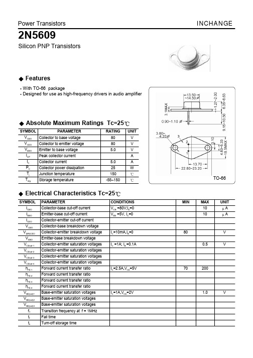
TO-66
Electrical Characteristics Tc=25
SYMBOL ICBO IEBO ICEO VCBO V(BR)CEO VEBO VCEsat-1 VCEsat-2 VCEsat-3 VCEsat-4 hFE-1 hFE-2 hFE-3 hFE-4 VBE(sat)1 VBE(sat)2 VBE(sat)3 fT tf ts PARAMETER Collector-base cut-off current Emitter-base cut-off current Collector-emitter cut-off current Collector-base breakdown voltage Collector-emitter breakdown voltage Emitter-base breakdown voltage Collector-emitter saturation voltages Collector-emitter saturation voltages Collector-emitter saturation voltages Collector-emitter saturation voltages Forward current transfer ratio Forward current transfer ratio Forward current transfer ratio Forward current transfer ratio Base-emitter saturation voltages Base-emitter saturation voltages Base-emitter saturation voltages Transition frequency at f = 1MHz Fall time Tum-off storage time IC=1A,VCE=2V 1.0 V IC=2.5A,VCE=5V 70 200 IC =1A; IB =0.1A 0.5 V IC=10mA,IB=0 80 V CONDITIONS VCB =80V;IE=0 VEB =5V, IC=0 MIN MAX 10 10 UNIT A A
2N5089中文资料

Amplifier TransistorsNPN SiliconMAXIMUM RATINGSTHERMAL CHARACTERISTICSELECTRICAL CHARACTERISTICS (T = 25°C unless otherwise noted)OFF CHARACTERISTICS1.R θJA is measured with the device soldered into a typical printed circuit board.2.Pulse Test: Pulse Width ≤ 300 m s, Duty Cycle ≤ 2.0%.ON Semiconductor t© Semiconductor Components Industries, LLC, 20011Publication Order Number:2N50882N5089COLLECTOR21EMITTERELECTRICAL CHARACTERISTICS (T= 25°C unless otherwise noted) (Continued)SMALL–SIGNAL CHARACTERISTICS2.Pulse Test: Pulse Width ≤ 300 m s, Duty Cycle ≤ 2.0%.Figure 2. Effects of Frequencyf, FREQUENCY (Hz)7.01020305.0Figure 3. Effects of Collector CurrentI C , COLLECTOR CURRENT (mA)Figure 4. Noise Currentf, FREQUENCY (Hz)Figure 5. Wideband Noise FigureR S , SOURCE RESISTANCE (OHMS)3.0NOISE CHARACTERISTICS(V CE = 5.0 Vdc, T A = 25°C)NOISE VOLTAGEe n , N O I S E V O L T A G E (n V )e n , N O IS E V O L T A G E (n V )I n , N O I S E C U R R E N T (p A )N F , N O I S E F I G U R E (d B )7.01020305.03.0100.10.20.31.00.72.03.05.07.004.08.0121620100 Hz NOISE DATA3002001003.05.07.010********R S , SOURCE RESISTANCE (OHMS)V T , T O T A L N O I S E V O L T A G E (n V )N F , N O I S E F I G U R E (d B )4.08.01220Figure 6. Total Noise Voltage R S , SOURCE RESISTANCE (OHMS)Figure 7. Noise Figure0.5Figure 8. DC Current GainI C , COLLECTOR CURRENT (mA)0.41.02.03.04.00.3h , D C C U R R E N T G A I N (N O R M A L I Z E D )0.2F E 0.70.5Figure 9. “On” VoltagesI C , COLLECTOR CURRENT (mA)0.40.60.81.00.2Figure 10. Temperature CoefficientsI C , COLLECTOR CURRENT (mA)V , V O L T A G E (V O L T S )-ā0.8-ā1.2-ā1.6-ā2R V B E ,B A S E -E M I T T E R θT E M P ER A T U R E C O E F F I C I E N T (m V /C )°-ā0.4-ā2.0f T , C U R R E N T -G A I N Ċ B A N D W I D T H P R O D U C T (M H z )C , C A P A C I T A N C E (p F )8.00.81.02.03.04.06.05003002007050100Figure 11. Capacitance V R , REVERSE VOLTAGE (VOLTS)Figure 12. Current–Gain — Bandwidth ProductI C , COLLECTOR CURRENT (mA)PACKAGE DIMENSIONSCASE 29–11ISSUE ALTO–92 (TO–226)NOTES:1.DIMENSIONING AND TOLERANCING PER ANSI Y14.5M, 1982.2.CONTROLLING DIMENSION: INCH.3.CONTOUR OF PACKAGE BEYOND DIMENSION R IS UNCONTROLLED.4.LEAD DIMENSION IS UNCONTROLLED IN P AND BEYOND DIMENSION K MINIMUM.PLANEDIM MIN MAX MIN MAX MILLIMETERSINCHES A 0.1750.205 4.45 5.20B 0.1700.210 4.32 5.33C 0.1250.165 3.18 4.19D 0.0160.0210.4070.533G 0.0450.055 1.15 1.39H 0.0950.105 2.42 2.66J 0.0150.0200.390.50K 0.500---12.70---L 0.250--- 6.35---N 0.0800.105 2.04 2.66P ---0.100--- 2.54R 0.115--- 2.93---V0.135--- 3.43---EMITTER2.BASE3.COLLECTORON Semiconductor and are trademarks of Semiconductor Components Industries, LLC (SCILLC). SCILLC reserves the right to make changes without further notice to any products herein. SCILLC makes no warranty, representation or guarantee regarding the suitability of its products for any particular purpose, nor does SCILLC assume any liability arising out of the application or use of any product or circuit, and specifically disclaims any and all liability, including without limitation special, consequential or incidental damages. “Typical” parameters which may be provided in SCILLC data sheets and/or specifications can and do vary in different applications and actual performance may vary over time. All operating parameters, including “Typicals” must be validated for each customer application by customer’s technical experts. SCILLC does not convey any license under its patent rights nor the rights of others.SCILLC products are not designed, intended, or authorized for use as components in systems intended for surgical implant into the body, or other applications intended to support or sustain life, or for any other application in which the failure of the SCILLC product could create a situation where personal injury or death may occur. Should Buyer purchase or use SCILLC products for any such unintended or unauthorized application, Buyer shall indemnify and hold SCILLC and its officers, employees, subsidiaries, affiliates, and distributors harmless against all claims, costs, damages, and expenses, and reasonable attorney fees arising out of, directly or indirectly, any claim of personal injury or death associated with such unintended or unauthorized use, even if such claim alleges that SCILLC was negligent regarding the design or manufacture of the part. SCILLC is an Equal Opportunity/Affirmative Action Employer. PUBLICATION ORDERING INFORMATIONJAPAN: ON Semiconductor, Japan Customer Focus Center4–32–1 Nishi–Gotanda, Shinagawa–ku, Tokyo, Japan 141–0031Phone: 81–3–5740–2700Email: r14525@。
L298电机驱动芯片资料

L298Jen uary 2000DUAL FULL-BRIDGE DRIVERMultiwatt15ORDERING NUMBERS :L298N (MultiwattVert.L298HN (MultiwattHori z. L298P (PowerSO20BLOCK DIAGRAM.OPERATING SUPPLY VOLTAGE UP TO 46V . TOTAL DC CURRENT UP TO4A . LOW SATURATION VOLTAGE.OVERTEMPERATURE PROTECTIONLOGICAL ” 0” INPUT VOLTAGE UP TO 1.5V (HIGHNOISE IMMUNITYDESCRIPTIONThe L298is an integrated monolithic circuit in a 15-lead Multiwatt andPowerSO20packages. It is a high voltage, high current dual full-bridge driver de-signedto acceptsta ndardTTL logic levels an ddrive in ductive loads such as relays, sole no ids, DC and stepp in gmotors. Two en able in puts are provided to en ableor disablethe device in depe nden tlyof the in-put sig nals. The emitters of the lower tran sistors of each bridge are conn ected togethera nd the corre-sp onding exter nal termi nal can be used for the con-n ecti onof an exter nalse nsing resistor.A nadditi onal supply in put is provided so that the logic works at a lower voltage.PowerSO201/13PIN CONNECTIONS (topviewGND Input 2VSS N.C. Out 1V S Out 2ln put 1En able A Sense AGND1089765432131415161719182012111GNDD95IN239In put 3En able B Out 3lnput 4Out 4N.C. Se nse B GND ABSOLUTE MAXIMUM RATINGSSymbol ParameterValue Un it V S Power Supply 50V V SS Logic Supply Voltage 7V V I ,V en In put and En able Voltage-0.3to 7V I OPeak Output Current (eachChanneFNon Repetitive (t=100 s 卩-Repetitive(80%on -20%off; t on =10ms -DCOperatio n 32.52A A A V sensSensing Voltage—to 2.3V P tot Total Power Dissipatio n (Tease =75C 25W T op Ju nctionOperating Temperature-25to 130 CT stg , T jStorage and Junction Temperature-40to 150°CTHERMAL DATASymbol ParameterPowerSO20Multiwatt15Unit R th j-case Thermal Resista nee Junction-case Max—°C/WR th j-amb Thermal Resista nee Jun cti on-ambie ntMax.13(*350C/W(*M oun ted on alumi num substrate1234567910118ENABLE B INPUT 3LOGIC SUPPLY VOLTAGE V SS GND INPUT 2ENABLE A INPUT 1 SUPPLY VOLTAGE V S OUTPUT 2OUTPUT 1CURRENT SENSING ATAB CONNECTED TO PIN 813141512CURRENT SENSING B OUTPUT4OUTPUT 3INPUT 4D95IN240AMultiwatt15PowerSO20L2982/13PIN FUNCTIONS (referto the block diagramMW.15PowerSO Name Fun ction1;152;19Se nse A; Sense B Betwee n this pin and ground is conn ected the sense resistor to control the current of the load.2;34;5Out 1; Out 2Outputs of the Bridge A; the curre nt that flows through the load conn ected betwee n these two pins is monitored at pin 1.46V SSupply Voltage for the Power Output Stages.A non-i nductive 100nF capacitor must be conn ected betwee n this pin and ground.5;77;9I nput 1; I nput 2TTL Compatible In puts of the Bridge A.6;118;14E nable A; En able BTTL Compatible En able In put:the L state disables the bridge A (en ableA an d/orthe bridge B (en ableB. 81,10,11,20GND Grou nd.912VSS Supply Voltage for the Logic Blocks. A100 nF capacitor must be conn ected between this pin and grou nd. 10; 1213;15I nput 3; I nput 4TTL Compatible In puts of the Bridge B.13; 1416;17Out 3; Out 4Outputs of the Bridge B. The curre nt that flows through the load conn ected betwee n these two pins is mon itored at pin 15—3;18N.C.Not Conn ectedELECTRICAL CHARACTERISTICS (VS =42V; V SS =5V, T j =25 C; unl ess otherwise specifiedSymbol ParameterTest Con diti onsMin. Typ.Max. Unit V S Supply Voltage (pin4 Operative ConditionV IH +2.546V V SS Logic Supply Voltage (pin9 4.557V I SQuiesce nt Supply Curre nt (pin4V en =H; I L =0V i =L V i =H 13502270mA mA V en =LVi =X 4mA ISSQuiesce nt Curre nt from V SS (pi n9 V en =H; I L =0V i =L V i =H 2473612mA mA V en =LV i =X6mA V iL In put Low Voltage (pi ns5, 7, 10, 12 —.31.5V V iH In put High Voltage (pi ns5, 7, 10, 12 2.3VSS V I iL Low Voltage In put Curre nt (pi ns5, 7, 10, 12V i =L-0 叭I iH High Voltage In put Curre nt (pin s5, 7, 10, 12Vi =H < V SS0.6V30100 叭V en =L Enable Low Voltage (pins6, 11 -0.31.5V V en =H Enable High Voltage (pin s6, 11 2.3V SS V I en =L Low Voltage En able Curre nt (pin s6, 11V en =L-0 叭I en =HHigh Voltage En able Curre nt (pin s6, 11V en =H < V SS0.6V30100 A V CEsat (HSource Saturation Voltage I L =1A I L =2A 0.951.3521.72.7V V V CEsat (LSink Saturation Voltage I L =1A (51 L =2A (50.851.21.71.62.3V V V CEsat Total Drop1 L =1A (5I L =2A(51.803.24.9V V V sensSensing Voltage (pin s1, 15-(12V L2983/13Figure 1:Typical Saturation Voltage vs. OutputCurre nt.Figure 2:Switching Times Test Circuits.Note :For INPUT Switchi ng, set EN =HFor ENABLESwitchi ng, set IN =H1 1Sensing voltage can be- 1V for t < 50 卩sec; in steady state V senOmV.2 >-See fig. 2.3 See fig. 4.4 The load must be a pure resistor.ELECTRICAL CHARACTERISTICS (continuedSymbol ParameterTest Con diti onsMi n.Typ. Max.Unit T 1(Vi Source Curre nt Turn-off Delay 0.5V i to 0.9I L (2;(41.5 s T 2(Vi 卩Source Current Fall Time 0.9I L to 0.1I L (2;(40.2 s T 3(Vi Sourc g Current Turn-onDelay 0.5V i to 0.1I L (2;(42 s T 4(Vi (Source Current Rise Time 0.1I L to 0.9I L(2;(40.7 s T 5(Vi Sink Current Turn-off Delay 0.5V i to 0.9I L (3;(40.7 s T 6(Vi Sink (Current Fall Time 0.9I L to 0.1I L (3;(40.25 s T 7(Vi Sink(Current Turn-on Delay 0.5V ito 0.9I L (3;(41.6 s T 8(Vi Sink Current Rise Time 0.1I L to 0.9I L (3;(40.2 s fc (Vi Commutation Frequency I L =2A 2540KHz T 1(Ven Source CurrentTurn-off Delay 0.5V en to 0.9I L (2;(43 s T 2(Ven Source Current Fall Time 0.9I L to0.1I L (2;(41 s T(3(Ven Source Current Turn-on Delay 0.5V en to 0.1I L (2;(40.3 s T ( 4(Ven Source Current Rise Time 0.1I L to 0.9I L (2;(40.4 s T 5(Ven Sink (Current Turnoff Delay 0.5V en to 0.9I L (3;(42.2 s T 6(Ven Sink Current Fall Time 0.9I L to 0.1I L(3;(40.35 s T 7(Ven Sink Current Turn-on Delay 0.5V en to 0.9I L (3;(40.25 s T 8(Ven ( Sink Curre nt Rise Time0.11 L to 0.91 L(3;(40.1pSL2984/13Figure 3:Source Current Delay Times vs. Input or Enable Switching. Figure 4:Switching Times Test Circuits.Note :For INPUT Switchi ng, set EN =HFor ENABLE Switching, set IN =LL2985/13Figure 5:Sink Current Delay Times vs. Input 0V Enable Switching. Figure 6:Bidirectio nal DC Motor Con trol.L =LowH =HighX =Don' tcareIn putsFunction V en =HC =H ;D =L Forward C =L ; D =H Reverse C =DFast Motor Stop V en =LC =X ;D =XFree Running Motor StopL2986/13Figure 7:For higher curre nts, outputs can be paralleled. Take care to parallel cha nnel 1with cha nnel 4and cha nnel 2with cha nnel 3.APPLICATION INFORMATION (Referto the block diagram 1.1. POWER OUTPUT STAGE TheL298i ntegratestwopoweroutputstages(A;B.The power output stage is a bridge configuration and its outputs can drive an in ductive load incom-mon or differe nzialmode, depe ndingon thestate of the in puts. The curre nt that flows through the loadcomes out from the bridge at the sense output :anexternalresistor (RSA ; R SB . allows to detect the in-tensity of this current.12 INPUT STAGE Each bridge is drive n by means of four gatesthe in-put of which are In1; In2; EnA and In3; In4; EnB. The In in putsset thebridge state whe n The En in put is high; a lowstateof theE n in puti nhibitsthe bridge. All the in puts are TTL compatible. 2. SUGGESTIONSA non inductive capacitor, usually of 100nF, mustbe foresee n betwee n both Vs and Vss, to ground.as n ear as possible to GND pin. Whe n the large ca-pacitor of the power supply is too far from the IC, a sec ond smaller one must be foresee n n ear the L298. The sense resistor, not of a wire wound type, mustbe groun ded near the n egative pole of Vs that must be n ear the GND pin of the I.C. Each in put must be conn ected to the source of thedriv ing sig nals by means of a very short path. Turn-On and Turn-Off :Before to Turn-0 NtheSup-plyVoltagea nd beforeto Turnit OFF,the En able in-put must be drive n to the Low state. 3. APPLICATIONS Fig 6shows a bidirectio nal DC motor con trolSche- matic Diagram for which only one bridge is n eeded. The exter nal bridge of diodes D1to D4is made byfour fast recovery eleme nts (trr < 200n sec that must be chose n of a VF as low as possible at theworst case of the load curre nt. The sen seoutputvoltage can be used to con trolthe curre nt amplitude by chopp ing the in puts,or to pro-vide overcurre nt protecti on by switchi ng low the en-able in put. The brake fun ctio n (Fastmotor stop requires that the Absolute Maximum Rat ing of 2Amps must n ever be overcome. When the repetitive peak curre nt n eeded from theload is higher than 2Amps, a paralleled configura-tion can be chosen (SeeFig.7. An exter nal bridge of diodes are required whe n in-ductive loads are drive n and whe n the in puts of the ICare chopped; Shottkydiodeswould bepreferred.L2987/13This solution can drive until 3AmpsIn DC operation and until 3.5Amps of a repetitive peak curre nt. OnFig 8it is show nthedriv ing ofa twophasebipolar stepper motor ; the n eeded sig nals to drive the in-puts of the L298are gen erated, in this example, from the IC L297.Fig 9shows an example of P.C.B. designed for the application of Fig 8.Fig 10shows a sec ond two phase bipolar stepper motor con trol circuit where the curre nt is con trolled by the I.C. L6506.Figure 8:Two Phase Bipolar Stepper Motor Circuit.This circuit drives bipolar stepper motors with winding currents up to 2A. The diodes are fast 2A types. R S仁R S2=0.5?D1to D8=2A Fast diodes{V F < 1.2V @I =2A trr < 200nsL2988/13Figure 9:SuggestedPrinted Circuit Board Layout for the Circuit of fig. 8(1:1scale.Figure 10:Two Phase Bipolar Stepper Motor Con trol Circuit by Using the Curre nt Con troller L6506. R R and R sense depe nd from the load curre ntL2989/13Multiwatt15VDIM. mminch MIN.TYP.MAX. MIN.TYP.MAX. A 50.197 B 2.650.104C 1.60.063D 10.039E 0.490.550.0190.022F 0.660.750.0260.030G1.021.271.520.0400.0500.060G117.5317.7818.030.6900.7000.710H119.60.772H220.20.795L 21.922.222.50.8620.8740.886L121.722.122.50.8540.8700.886 L217.6518.10.6950.713L317.2517.517.750.6790.6890.699L410.310.710.90.4060.4210.429L72.652.90.1040.114 M 4.254.554.850.1670.1790.191M14.635.085.530.1820.2000.218S1.92.60.0750.102S11.92.60.0750.102Dia13.653.850.1440.152OUTLINE AND MECHANICAL DATAL29810/13L298 DIM. MIN. A B C E F G G1 H1 H2 L L1 L2 L3 L4 L5 L6 L7 S S1 Dia1 2.651.9 1.9 3.65 17.25 10.3 20.57 18.032.54 17.5 10.7 5.28 2.38 2.9 2.6 2.63.85 0.104 0.0750.075 0.144 17.75 10.9 0.679 0.406 0.49 0.66 1.14 17.57 19.6 20.2 0.810 0.710 0.1000.689 0.421 0.208 0.094 0.114 0.102 0.102 0.152 0.699 0.429 1.27 17.78 mm TYP.MAX. 5 2.65 1.6 0.55 0.75 1.4 17.91 0.019 0.026 0.045 0.692 0.772 0.795 0.050 0.700MIN. i nch TYP. MAX. 0.197 0.104 0.063 0.022 0.030 0.055 0.705 OUTLINE ANDMECHANICAL DATA Multiwatt15 H 11/13L298 mm TYP. i nch TYP. DIM. A a1 a2 a3 b c D (1 D1 E e e3 E1 (1 E2 E3 G H hL N S T MIN. 0.1 0 0.4 0.23 15.8 9.4 13.9 MAX. 3.6 0.3 3.3 0.1 0.53 0.32 16 9.8 14.5MIN. 0.004 0.000 0.016 0.009 0.622 0.370 0.547 MAX. 0.142 0.012 0.130 0.004 0.0210.013 0.630 0.386 0.570 OUTLINE AND MECHANICAL DATA 1.27 11.43 10.9 5.8 015.5 0.8 11.1 0.429 2.9 6.2 0.228 0.1 0.000 15.9 0.610 1.1 1.1 0.031 1Qmax. 8 (max. °10 0.050 0.450 0.437 0.114 0.244 0.004 0.626 0.043 0.043 JEDEC MO66 0.394 (1 ” Dand F ” do not include mold flash or protrusio. - Mold flash or protrusions shall notexceed 0.15 mm (0.006 - Critical dimensions: ” E” , ” G' and ” a3” PowerSO20 N N a2 b e A R c DETAIL B a1 E DETAIL A DETAIL A e3 H lead D a3 DETAIL B 20 11 GagePla ne 0.35 slug -C- S E2 T E1 BOTTOM VIEW L SEATING PLANE G C (COPLANARITY E3 1 10 h x 45 PSO20MEC D1 12/13。
阿布拉康UHF RFID标签说明书
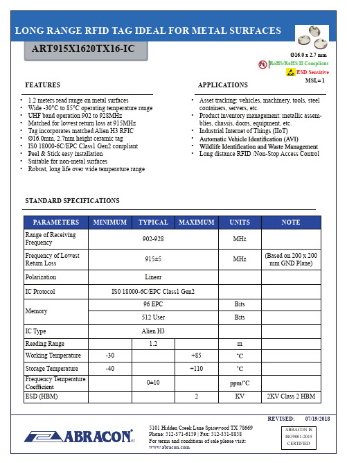
Pb RoHS/RoHS II CompliantMSL= 1REVISED:07/19/2018ESD SensitiveØ16.0 x 2.7 mmSTANDARD SPECIFICATIONS FEATURES APPLICATIONS• 1.2 meters read range on metal surfaces• Wide -30°C to 85°C operating temperature range • UHF band operation 902 to 928MHz• Matched for lowest return loss at 915MHz • Tag incorporates matched Alien H3 RFIC • Ø16.0mm, 2.7mm height ceramic tag• IS0 18000-6C/EPC Class1 Gen2 compliant • Peel & Stick easy installation • Suitable for non-metal surfaces•Robust, long life over wide temperature range• Asset tracking: vehicles, machinery, tools, steel containers, servers, etc.• Product inventory management: metallic assem-blies, chassis, doors, equipment, etc.• Industrial Internet of Things (IIoT) • •• Long distance RFID /Non-Stop Access ControlPARAMETERS MINIMUM TYPICAL MAXIMUM UNITS NOTERange of Receiving Frequency902-928MHz Frequency of Lowest Return Loss 915±5MHz(Based on 200 x 200 mm GND Plane)Polarization LinearIC Protocol IS0 18000-6C/EPC Class1 Gen2Memory 96 EPC Bits 512 User BitsIC Type Alien H3Reading Range 1.2m Working Temperature -30+85Storage Temperature -40+110Frequency Temperature 0±10ESD (HBM)2KV2KV Class 2 HBMPb RoHS/RoHS II CompliantMSL= 1REVISED:07/19/2018ESD SensitiveØ16.0 x 2.7 mmMECHANICAL DIMENSIONS (ALL DIMENSIONS ARE IN mm)PACKAGINGMounting: Mounted with adhesive/tape (not included).PACKAGE TYPE QUANTITY Tray 60 pcs/tray Vacuum Bag 300pcs/ Vacuum BagMOQ300pcsTRAYTrayPb RoHS/RoHS II CompliantMSL= 1REVISED:07/19/2018ESD SensitiveØ16.0 x 2.7 mmNOTES1. 2.to modify prior to an order placement.3. In no case shall ABRACON be liable for any product failure from in appropriate handling or operation of4.5.-reliability where component failure could result in loss of life and/or property damage.CAUTION1. Do not apply excess mechanical stress to the component body or terminations. Do not attempt to re-form or bend the components as this will cause damage to the component.2.3.in-circuit validation is recommended.4. Electrostatic sensitive device; observe standard precautions for handling.。
2N5087中文资料

2N5087中⽂资料Amplifier TransistorPNP SiliconMAXIMUM RATINGSTHERMAL CHARACTERISTICSELECTRICAL CHARACTERISTICS (T = 25°C unless otherwise noted)OFF CHARACTERISTICS1.Pulse T est: Pulse Width ≤ 300 m s, Duty Cycle ≤2.0%.Preferred devices are ON Semiconductor recommended choices for future use and best overall value. ON Semiconductor tPublication Order Number:2N5087ON Semiconductor Preferred Device COLLECTOR21EMITTERELECTRICAL CHARACTERISTICS (T= 25°C unless otherwise noted) (Continued)1.Pulse T est: Pulse Width ≤ 300 m s, Duty Cycle ≤2.0%.TYPICAL NOISE CHARACTERISTICS(V CE = –5.0 Vdc, T A = 25°C)Figure 1. Noise Voltage f, FREQUENCY (Hz)5.07.0103.0Figure 2. Noise Currentf, FREQUENCY (Hz)1.01020100200500 1.0?k 2.0?k5.0?k10?ke n , N O I S E V O L T A G E (n V )102050100200500 1.0?k 2.0?k 5.0?k10?k2.0NOISE FIGURE CONTOURS(V CE = –5.0 Vdc, T A = 25°C)500?k 1002005001.0?k 10?k 5.0?k 20?k 50?k 100?k 200?k 2.0?k 1.0?M 500?k 1002005001.0?k 10?k 5.0?k 20?k 50?k 100?k 200?k 2.0?k 1.0?M Figure 3. Narrow Band, 100 Hz I C , COLLECTOR CURRENT (µA)Figure 4. Narrow Band, 1.0 kHzI C , COLLECTOR CURRENT (µA)10R S , S O UR CE R E S I S T A N C E (O H M S )R S , S O U R C E R E S I S T A N C E (O H M S )Figure 5. WidebandI C , COLLECTOR CURRENT (µA)10R S , S O U R C E R E S I S T A N C E (O H M S )Noise Figure is Defined as:NF +20log 10e n 2)4KTR S )I n 2R S 24KTR S1ń2= Noise Voltage of the Transistor referred to the input. (Figure 3)= Noise Current of the Transistor referred to the input. (Figure4)= Boltzman’s Constant (1.38 x 10⁻²³ j/°K)= T emperature of the Source Resistance (°K)= Source Resistance (Ohms)e n I n K T R S 203050701002003005007001.0?k10203050701002003005007001.0?k500?k 1002005001.0?k 10?k 5.0?k 20?k 50?k 100?k 200?k 2.0?k 1.0?M 203050701002003005007001.0?kh , D C C U R R E N T G A I NF E I C , COLLECTOR CURRENT (mA)1.4I C , COLLECTOR CURRENT (mA)V , V O L T A G E (V O L T S )Figure 9. “On” Voltages 0.40.60.81.00.2V C E , C O L L E C T O R -E M I T T E R V O L T A G E (V O L T S ) Figure 10. Temperature Coefficients1.21.00.80.60.40.20C , C A P A C I T A N C E (p F )Figure 11. Turn–On TimeI C , COLLECTOR CURRENT (mA)500Figure 12. Turn–Off TimeI C , COLLECTOR CURRENT (mA)Figure 13. Current–Gain — Bandwidth Product I C , COLLECTOR CURRENT (mA)Figure 14. Capacitance V R , REVERSE VOLTAGE (VOLTS)Figure 15. Input Impedance I C , COLLECTOR CURRENT (mA)Figure 16. Output AdmittanceI C , COLLECTOR CURRENT (mA)5000.510t , T I M E (n s )f ?, C U R R E N T -G A I N ? B A N D W I D T H P R O D U C T (M H z )T h i e , I N P U T I M P E D A N C E (k )5.07.010203050701003005070100200300 1.02.03.05.07.00.20.30.50.71.02.03.05.07.01020200-5.0-7.0-50-70Figure 17. Thermal Responset, TIME (ms)1.0r (t ) T R A N S I E N T T H E R M A L R E S I S T A N C E (N O R M A L I Z E D ) 0.010.020.030.050.070.10.20.30.50.750?kT J , JUNCTION TEMPERATURE (°C)104I C , C O L L E C T O R C U R R E N T (n A )Figure 19. Typical Collector Leakage Current400I C , C O L L E C T O R C U R R E N T (m A )DESIGN NOTE: USE OF THERMAL RESPONSE DATAA train of periodical power pulses can be represented by the model as shown in Figure 19. Using the model and the device thermal response the normalized effective transient thermal resistance of Figure 17 was calculated for various duty cycles. To find Z θJA(t), multiply the value obtained from Figure 17 by the steady state value R θJA .Example:The 2N5087 is dissipating 2.0 watts peak under the follow-ing conditions:t 1 = 1.0 ms, t 2 = 5.0 ms (D = 0.2)Using Figure 17 at a pulse width of 1.0 ms and D = 0.2, the reading of r(t) is 0.22.The peak rise in junction temperature is thereforeT = r(t) x P (pk) x R θJA = 0.22 x 2.0 x 200 = 88°C.For more information, see ON Semiconductor Application Note AN569/D, available from the Literature Distribution Center or on our website at/doc/08656144e518964bcf847c95.html .The safe operating area curves indicate I C –V CE limits of the transistor that must be observed for reliableoperation.Collector load lines for specific circuits must fall below the limits indicated by the applicable curve.The data of Figure 18 is based upon T J(pk) = 150°C; T C or T A is variable depending upon conditions. Pulse curves are valid for duty cycles to 10% provided T J(pk) ≤ 150°C. T J(pk)may be calculated from the data in Figure 17. At high case or ambient temperatures, thermal limitations will reduce the power than can be handled to values less than the limitations imposed by second breakdown.10-210-11001011021034.06.010204060100200PACKAGE DIMENSIONSCASE 29–11ISSUE ALTO–92 (TO–226)NOTES:1.DIMENSIONING AND TOLERANCING PER ANSI Y14.5M, 1982.2.CONTROLLING DIMENSION: INCH.3.CONTOUR OF PACKAGE BEYOND DIMENSION R IS UNCONTROLLED.4.LEAD DIMENSION IS UNCONTROLLED IN P AND BEYOND DIMENSION K MINIMUM.DIM MIN MAX MIN MAX MILLIMETERSINCHES A 0.1750.205 4.45 5.20B 0.1700.210 4.32 5.33C 0.1250.165 3.18 4.19D 0.0160.0210.4070.533G 0.0450.055 1.15 1.39H 0.0950.105 2.42 2.66J 0.0150.0200.390.50K 0.500---12.70---L 0.250--- 6.35---N 0.0800.105 2.04 2.66P ---0.100--- 2.54R 0.115--- 2.93---V0.135--- 3.43---EMITTER2.BASE3.COLLECTORON Semiconductor and are trademarks of Semiconductor Components Industries, LLC (SCILLC). SCILLC reserves the right to make changes without further notice to any products herein. SCILLC makes no warranty, representation or guarantee regarding the suitability of its products for any particular purpose, nor does SCILLC assume any liability arising out of the application or use of any product or circuit, and specifically disclaims any and all liability, including without limitation special, consequential or incidental damages. “Typical” parameters which may be provided in SCILLC data sheets and/or specifications can and do vary in different applications and actual performance may vary over time. All operating parameters, including “Typicals” must be validated for each customer application by customer’s technical experts. SCILLC does not convey any license under its patent rights nor the rights of others.SCILLC products are not designed, intended, or authorized for use as components in systems intended for surgical implant into the body, or other applications intended to support or sustain life, or for any other application in which the failure of the SCILLC product could create a situation where personal injury or death may occur. Should Buyer purchase or use SCILLC products for any such unintended or unauthorized application, Buyer shall indemnify and hold SCILLC and its officers, employees, subsidiaries, affiliates, and distributors harmless against all claims, costs, damages, and expenses, and reasonable attorney fees arising out of, directly or indirectly, any claim of personal injury or death associated with such unintended or unauthorized use, even if such claim alleges that SCILLC was negligent regarding the design or manufacture of the part. SCILLC is an Equal Opportunity/Affirmative Action Employer. PUBLICATION ORDERING INFORMATION JAPAN: ON Semiconductor, Japan Customer Focus Center4–32–1 Nishi–Gotanda, Shinagawa–ku, Tokyo, Japan 141–0031Phone: 81–3–5740–2700Email: r14525@/doc/08656144e518964bcf847c95.html。
Pololu双VNH5019电机驱动板 дляArduino说明书

Features
Pololu dual VNH5019 motor driver shield, assembled and connected to an Arduino
Uno R3.
Pololu dual VNH5019 motor driver shield for Arduino, bottom view with board dimensions.
Can survive input voltages up to 41 V Undervoltage and overvoltage shutdown High-side and low-side thermal shutdown Short-to-ground and short-to-Vcc protection
1 While the overvoltage protection typically kicks in at 27 V, it can trigger at voltages as low as 24 V, so we do not recommend using this motor driver with 24 V batteries, which significantly exceed 24 V when fully charged. If the shield is configured to power an Arduino or Arduino clone, the supply voltage must conform to that Arduino’s input voltage requirements.
Overview
Pololu Dual VNH5019 Motor Driver Shield for Arduino
拉雷尔电子有限公司产品说明书
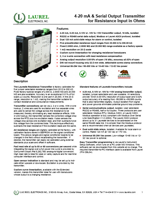
LAUREL ELECTRONICS, INC.4-20 mA & Serial Output Transmitter for Resistance Input in OhmsFeatures•4-20 mA, 0-20 mA, 0-10V or -10V to +10V transmitter output, 16 bits, isolated•RS232 or RS485 serial data output, Modbus or Laurel ASCII protocol, isolated•Dual 120 mA solid state relays for alarm or control, isolated•Five precalibrated resistance input ranges from 20.000 Ω to 200.00 kΩ•Fixed 2.0000 ohm, 2.0000 MΩ and 20.000 MΩ range available as a factory specia• 1 mΩ resolution on 20 Ω scale•Custom curve linearization for changing resistance transducers•2, 3 or 4-wire connection with lead resistance compensation•Analog output resolution 0.0015% of span (16 bits), accuracy ±0.02% of span•DIN rail mount housing only 22.5 mm wide, detachable screw-clamp connectors•Universal 85-264 Vac / 90-300 Vdc or 10-48 Vdc / 12-32 Vac powerDescriptionThe Laureate Resistance Transmitter is factory calibrated forfive jumper selectable resistance ranges from 20 Ω to 200 kΩ.Fixed factory-special ranges of 2.000 Ω, 2.0000 MΩ and 20.000MΩ are also available. Accuracy is an exceptional 0.01% of fullscale ± 2 counts. Resolution is one part in 20,000. In the 20 Ωrange, resolution is 1 mΩ, making the transmitter suitable forcontact resistance and conductance measurements.Transmitter connections can be via 2, 3 or 4 wires. With 4-wirehookup, 2 wires are used for excitation and two separate wiresare used to sense the voltage across the resistance to bemeasured, thereby eliminating any lead resistance effects. With3-wire hookup, the transmitter senses the combined voltage dropacross the RTD plus two excitation leads. It also senses thevoltage drop across one excitation lead, and then subtracts twicethis voltage from the combined total. This technique effectivelysubtracts the lead resistance if the excitation leads are the same.All resistance ranges are digitally calibrated at the factory, withcalibration factors stored in EEPROM on the signal conditionerboard. This allows ranges and signal conditioner boards to bechanged in the field without recalibrating the transmitter. Ifdesired, the transmitter can easily be calibrated using externalstandards plus scale and offset in software.Fast read rate at up to 50 or 60 conversions per second whileintegrating the signal over a full power line cycle is provided byConcurrent Slope (Pat 5,262,780) analog-to-digital conversion.High read rate is ideal for peak or valley capture and for real-timecomputer interface and control.Open sensor indication is standard and may be set up to indi-cate either upscale or downscale. Excitation is provided by thetransmitter.Custom curve linearization, available with the Extendedversion, makes this transmitter ideal for use with transducerswhose output is a changing resistance.Standard features of Laureate transmitters include:•4-20 mA, 0-10V or -10V to +10V analog transmitter output,isolated, jumper-selectable and user scalable. All selectionsprovide 16-bit (0.0015%) resolution of output span and 0.02%output accuracy of a reading from -99,999 to +99,999 countsthat is also transmitted digitally. Output isolation from signaland power grounds eliminates potential ground loop problems.•Serial communications output, isolated. User selectableRS232 or RS485, half or full duplex. Three protocols are userselectable: Modbus RTU, Modbus ASCII, or Laurel ASCII.Modbus operation is fully compliant with Modbus Over SerialLine Specification V1.0 (2002). The Laurel ASCII protocolallows up to 31 Laureate devices to be addressed on thesame RS485 data line. It is simpler than the Modbus protocoland is recommended when all devices are Laureates.•Dual solid state relays, isolated. Available for local alarm orcontrol. Rated 120 mA at 130 Vac or 170 Vdc.•Universal 85-264 Vac power. Low-voltage 10-48 Vdc or 12-32 Vac power is optional.Easy Transmitter programming is via Laurel's InstrumentSetup Software, which runs on a PC under MS Windows. Thissoftware can be downloaded from this website at no charge. Therequired transmitter-to-PC interface cable is available from Laurel(P/N CBL04).SpecificationsRange Resolution Accuracy Excitation Current0-2.0000 Ω 0-20.000 Ω 0-200.00 Ω 0-2000.0 Ω 0-20000 Ω 0-200.00 kΩ 0-2.0000 MΩ 0-20.000 MΩ 0.1 mΩ1 mΩ10 mΩ100 mΩ1 Ω10 Ω100 Ω1 kΩ±0.01% of range± 2 counts5 mA5 mA500 µA50 µA5 µA500 nA500 nA75 nASignal InputInput Resolution Input Accuracy Update Rate, Max 16 bits (65,536 steps)±0.01% of full scale ± 2 counts 50/sec at 50 Hz, 60/sec at 60 HzAnalog Output (standard)Output Levels Compliance at 20 mA Compliance at 10V Output Resolution Output Accuracy Output Isolation 4-20 mA, 0-20 mA, 0-10 Vdc, -10 to +10Vdc (user selectable) 10V (0-500Ω load)2 mA (5 kΩ load or higher)16 bits (65,536 steps)0.02% of output span plus conversion accuracy250V rms working, 2.3 kV rms per 1 minute testSerial Communications (standard)Signal TypesData RatesOutput Isolation Serial Protocols Modbus Modes Modbus Compliance Digital Addressing RS232 or RS485 (half or full duplex)300, 600, 1200, 2400, 4800, 9600, 19200 baud250V rms working, 2.3 kV rms per 1 min testModbus RTU, Modbus ASCII, Laurel ASCIIRTU or ASCIIModbus over Serial Line Specification V1.0 (2002)247 Modbus addresses. Up to 32 devices on an RS485 line w/o a repeater.Dual Relay Output (standard)Relay Type Load Rating Two solid state relays, SPST, normally open, Form A 120 mA at 140 Vac or 180 VdcPower InputStandard Power Low Power Option Power Frequency Power Isolation Power Consumption 85-264 Vac or 90-300 Vdc10-48 Vdc or 12-32 VacDC or 47-63 Hz250V rms working, 2.3 kV rms per 1 min test 2W typical, 3W with max excitation outputMechanicalDimensions MountingElectrical Connections 129 x 104 x 22.5 mm case35 mm rail per DIN EN 50022 Plug-in screw-clamp connectorsEnvironmentalOperating Temperature Storage Temperature Relative Humidity Cooling Required 0°C to 55°C-40°C to 85°C95% at 40°C, non-condensingMount transmitters with ventilation holes at top and bottom. Leave 6 mm (1/4") between transmitters, or force air with a fan.PinoutMechanicalQA Application with Relays in Passband ModeA deviation limit (50 mΩ in this example) is set uparound both sides of a setpoint. The relay closes (oropens) when the reading falls within the deviationband, and opens (or closes) when the reading fallsoutside of this band. This mode sets up a passbandaround the setpoint and can be used for contactresistance testing in a production environment.RTD HookupIn 4-wire hookup, different pairs of leads are used to apply the excitation current and sense the voltage drop across the unknown resistance, so that the IR drop across the excitation leads is not a factor.In 3-wire hookup, the transmitter senses the combined voltage drop across the unknown resistance plus two excitation leads. It also senses the voltage drop across one excitation lead, and then subtracts twice this voltage from the combined total. This technique effectively subtracts all lead resistance and compen-sates for ambient temperature changes if the two excitation leads are identical.In 2-wire hookup, the transmitter senses the combined voltage drop across the unknown resistance and both lead wires. The voltage drop across the lead wires can be measured by shorting out the resistance during transmitter setup, and this voltage is then automatically subtracted from the combined total. However, changing resistance of the lead wires due to ambient tempera-ture changes will not be compensated.Ordering GuideCreate a model a model number in this format: LT20R1Transmitter Type LT Laureate 4-20 mA & RS232/RS485 output transmitter Main Board 2 Standard Main BoardPower0 Isolated 85-264 Vac or 90-300 Vdc 1 Isolated 10-48 Vdc or 12-32 VacResistance RangeR0 0-20 ohms (factory special fixed range) R1 0-20 ohms R2 0-200 ohms R3 0-2 kohms R4 0-20 kohms R5 0-200 kohmsR6 0-2 Mohms (factory special fixed range) R7 0-20 Mohms (factory special fixed range)Note: The same signal conditioner board can be used for resistance and RTD temperature measurement.AccessoriesCBL04 RS232 cable, 7ft. Connects RS232 screw terminals of LT transmitter to DB9port of PC.CBL02 USB to RS232 adapter cable. Combination of CBL02 and CBL04 connectstransmitter RS232 terminals to PC USB port.。
- 1、下载文档前请自行甄别文档内容的完整性,平台不提供额外的编辑、内容补充、找答案等附加服务。
- 2、"仅部分预览"的文档,不可在线预览部分如存在完整性等问题,可反馈申请退款(可完整预览的文档不适用该条件!)。
- 3、如文档侵犯您的权益,请联系客服反馈,我们会尽快为您处理(人工客服工作时间:9:00-18:30)。
2N5088, 2N5089Amplifier TransistorsNPN SiliconFeatures•Pb−Free Packages are Available*MAXIMUM RATINGSRating Symbol Value UnitCollector − Emitter Voltage2N50882N5089V CEO3025VdcCollector − Base Voltage2N50882N5089V CBO3530VdcEmitter − Base Voltage V EBO 3.0Vdc Collector Current − Continuous IC50mAdcTotal Device Dissipation @ T A = 25°C Derate above 25°C P D6255.0mWmW/°CTotal Device Dissipation @ T C = 25°C Derate above 25°C P D 1.512WmW/°COperating and Storage JunctionTemperature RangeT J, T stg−55 to +150°C THERMAL CHARACTERISTICSCharacteristic Symbol Max Unit Thermal Resistance, Junction−to−Ambient(Note 1)R q JA200°C/W Thermal Resistance, Junction−to−Case R q JC83.3°C/WStresses exceeding Maximum Ratings may damage the device. Maximum Ratings are stress ratings only. Functional operation above the Recommended Operating Conditions is not implied. Extended exposure to stresses above the Recommended Operating Conditions may affect device reliability.1.R q JA is measured with the device soldered into a typical printed circuit board.*For additional information on our Pb−Free strategy and soldering details, please download the ON Semiconductor Soldering and Mounting Techniques Reference Manual, SOLDERRM/D.x = 8 or 9A = Assembly LocationY = YearWW = Work WeekG = Pb−Free PackageMARKING DIAGRAM3 COLLECTOR2BASE1 EMITTERDevice Package Shipping†2N5089G2N2089RLREORDERING INFORMATION†For information on tape and reel specifications, including part orientation and tape sizes, please refer to our T ape and Reel Packaging Specifications Brochure, BRD8011/D.TO−922000/Tape & ReelTO−92(Pb−Free)5000 Units/Bulk2N508xAYWW GG(Note: Microdot may be in either location)2N5088G TO−92(Pb−Free)5000 Units/Bulk2N2088RLRAG TO−92(Pb−Free)2000/Tape & Reel212BENT LEADTAPE & REELAMMO PACKSTRAIGHT LEADBULK PACKTO−92CASE 29STYLE 1ELECTRICAL CHARACTERISTICS (T A = 25°C unless otherwise noted)CharacteristicSymbolMinMaxUnitOFF CHARACTERISTICSCollector −Emitter Breakdown Voltage (Note 2)(I C = 1.0 mAdc, I B = 0)2N50882N5089V (BR)CEO3025−−VdcCollector −Base Breakdown Voltage (I C = 100 m Adc, I E = 0)2N50882N5089V (BR)CBO3530−−VdcCollector Cutoff Current (V CB = 20 Vdc, I E = 0)2N5088(V CB = 15 Vdc, I E = 0)2N5089I CBO−−5050nAdcEmitter Cutoff Current(V EB(off) = 3.0 Vdc, I C = 0)(V EB(off) = 4.5 Vdc, I C = 0)I EBO−−50100nAdcON CHARACTERISTICSDC Current Gain(I C = 100 m Adc, V CE = 5.0 Vdc)2N50882N5089(I C = 1.0 mAdc, V CE = 5.0 Vdc)2N50882N5089(I C = 10 mAdc, V CE = 5.0 Vdc) (Note 2)2N50882N5089h FE3004003504503004009001200−−−−−Collector −Emitter Saturation Voltage (I C = 10 mAdc, I B = 1.0 mAdc)V CE(sat)−0.5Vdc Base −Emitter On Voltage(I C = 10 mAdc, V CE = 5.0 Vdc) (Note 2)V BE(on)−0.8VdcSMALL−SIGNAL CHARACTERISTICS Current−Gain − Bandwidth Product(I C = 500 m Adc, V CE = 5.0 Vdc, f = 20 MHz)f T 50−MHz Collector−Base Capacitance(V CB = 5.0 Vdc, I E= 0, f = 1.0 MHz)C cb − 4.0pF Emitter−Base Capacitance(V EB = 0.5 Vdc, I C = 0, f = 1.0 MHz)C eb −10pF Small−Signal Current Gain(I C = 1.0 mAdc, V CE = 5.0 Vdc, f = 1.0 kHz)2N50882N5089h fe35045014001800−Noise Figure(I C = 100 m Adc, V CE = 5.0 Vdc, R S = 1.0 k W , f = 1.0 kHz)2N50882N5089NF−−3.02.0dB2.Pulse Test: Pulse Width ≤ 300 m s, Duty Cycle ≤ 2.0%.Figure 1. Transistor Noise ModelFigure 2. Effects of Frequencyf, FREQUENCY (Hz)7.01020305.0Figure 3. Effects of Collector CurrentI C , COLLECTOR CURRENT (mA)Figure 4. Noise Currentf, FREQUENCY (Hz)Figure 5. Wideband Noise FigureR S , SOURCE RESISTANCE (OHMS)3.010NOISE CHARACTERISTICS(V CE = 5.0 Vdc, T A = 25°C)NOISE VOLTAGEe n , N O I S E V O L T A G E (n V )e n , N O I S E V O L T A G E (n V )I n , N O I S E C U R R E N T (p A )N F , N O I S E F I G U R E (d B )20501002005001 k 2 k 5 k 10 k 20 k 50 k 100 k7.01020305.03.00.010.020.050.10.20.5 1.0 2.0 5.010101020501002005001 k 2 k 5 k 10 k 20 k 50 k 100 k 0.10.20.31.00.72.03.05.07.01020501002005001 k 2 k 5 k 10 k 20 k 50 k 100 k04.08.0121620100 Hz NOISE DATA3002001003.05.07.010********R S , SOURCE RESISTANCE (OHMS)1020501002005001 k 2 k 5 k 10 k 20 k 50 k 100 kV T , T O T A L N O I S E V O L T A G E (n V )N F , N O I S E F I G U R E (d B )4.08.0121620Figure 6. Total Noise Voltage 1020501002005001 k 2 k 5 k 10 k 20 k 50 k 100 kR S , SOURCE RESISTANCE (OHMS)Figure 7. Noise Figure0.5Figure 8. DC Current GainI C , COLLECTOR CURRENT (mA)0.41.02.03.04.00.3h , D C C U R R E N T G A I N (N O R M A L I Z E D )0.2F E 0.70.50.010.020.050.10.20.5 1.0 2.0 5.0102050100Figure 9. “On” VoltagesI C , COLLECTOR CURRENT (mA)0.40.60.81.00.2Figure 10. Temperature CoefficientsI C , COLLECTOR CURRENT (mA)V , V O L T A G E (V O L T S )0.010− 0.8− 1.2− 1.6− 2.4R V B E , B A S E −E M I T T E R θT E M P E R A T U R E C O E F F I C I E N T (m V /C )°− 0.4− 2.00.020.050.10.20.5 1.0 2.0 5.0102050100f T , CU R R E N T −G A I N Ċ B A N D WI D T H P R O D U C T (M H z )C , C A P A C I T A N C E (p F )8.00.81.02.03.04.06.00.10.20.5 1.0 2.0 5.01020501001.02.05.03.07.010203050701005003002007050100Figure 11. Capacitance V R , REVERSE VOLTAGE (VOLTS)Figure 12. Current−Gain — Bandwidth ProductI C , COLLECTOR CURRENT (mA)PACKAGE DIMENSIONSTO−92 (TO−226)CASE 29−11ISSUE AMNOTES:1.DIMENSIONING AND TOLERANCING PER ANSI Y14.5M, 1982.2.CONTROLLING DIMENSION: INCH.3.CONTOUR OF PACKAGE BEYOND DIMENSION R IS UNCONTROLLED.4.LEAD DIMENSION IS UNCONTROLLED IN P AND BEYOND DIMENSION K MINIMUM.PLANEDIM MIN MAX MIN MAX MILLIMETERSINCHES A 0.1750.205 4.45 5.20B 0.1700.210 4.32 5.33C 0.1250.165 3.18 4.19D 0.0160.0210.4070.533G 0.0450.055 1.15 1.39H 0.0950.105 2.42 2.66J 0.0150.0200.390.50K 0.500−−−12.70−−−L 0.250−−− 6.35−−−N 0.0800.105 2.04 2.66P −−−0.100−−− 2.54R 0.115−−− 2.93−−−V0.135−−−3.43−−−NOTES:1.DIMENSIONING AND TOLERANCING PER ASME Y14.5M, 1994.2.CONTROLLING DIMENSION: MILLIMETERS.3.CONTOUR OF PACKAGE BEYOND DIMENSION R IS UNCONTROLLED.4.LEAD DIMENSION IS UNCONTROLLED IN P AND BEYOND DIMENSION K MINIMUM.DIM MIN MAX MILLIMETERS A 4.45 5.20B 4.32 5.33C 3.18 4.19D 0.400.54G 2.40 2.80J 0.390.50K 12.70−−−N 2.04 2.66P 1.50 4.00R 2.93−−−V3.43−−−STYLE 1:PIN 1.EMITTER2.BASE3.COLLECTORON Semiconductor and are registered trademarks of Semiconductor Components Industries, LLC (SCILLC). SCILLC reserves the right to make changes without further notice to any products herein. SCILLC makes no warranty, representation or guarantee regarding the suitability of its products for any particular purpose, nor does SCILLC assume any liability arising out of the application or use of any product or circuit, and specifically disclaims any and all liability, including without limitation special, consequential or incidental damages.“Typical” parameters which may be provided in SCILLC data sheets and/or specifications can and do vary in different applications and actual performance may vary over time. All operating parameters, including “Typicals” must be validated for each customer application by customer’s technical experts. SCILLC does not convey any license under its patent rights nor the rights of others. SCILLC products are not designed, intended, or authorized for use as components in systems intended for surgical implant into the body, or other applications intended to support or sustain life, or for any other application in which the failure of the SCILLC product could create a situation where personal injury or death may occur. Should Buyer purchase or use SCILLC products for any such unintended or unauthorized application, Buyer shall indemnify and hold SCILLC and its officers, employees, subsidiaries, affiliates,and distributors harmless against all claims, costs, damages, and expenses, and reasonable attorney fees arising out of, directly or indirectly, any claim of personal injury or death associated with such unintended or unauthorized use, even if such claim alleges that SCILLC was negligent regarding the design or manufacture of the part. SCILLC is an Equal Opportunity/Affirmative Action Employer. This literature is subject to all applicable copyright laws and is not for resale in any manner.PUBLICATION ORDERING INFORMATION。