ECKD4A102MDU中文资料
4R182S1E5500;4R252S1E5500;4R252S1N5500;4R112S1E3500;4R182S1E3200;中文规格书,Datasheet资料
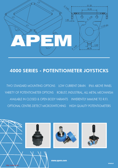
4000 SERIES - POTENTIOMETER JOYSTICKSTWO STANDARD MOUNTING OPTIONS LOW CURRENT DRAIN IP65 ABOVE PANEL VARIETY OF POTENTIOMETER OPTIONS ROBUST , INDUSTRIAL, ALL METAL MECHANISMAVAILABLE IN CLOSED & OPEN BODY VARIANTS INHERENTLY IMMUNE TO R.F .I.OPTIONAL CENTRE-DETECT MICROSWITCHING HIGH QUALITY POTENTIOMETERS51.2018.20R2.651.85R3.028.7510 d7.5i a3.60R4.5APEMAPEMGENERAL DESCRIPTIONThe 4000 Series is a range of robust, industrial quality potentiometer joysticks. All 4000 Series share the same, all metal, mechanism to provide the finest performance and service life over a wide range of temperatures and loads. All 4000 Series employ high quality plastic film potentiometers, yielding a service life of many millions of cycles.Whilst contactless joysticks such as the 9000 Series have replaced potentiometer joysticks in many applications, the 4000 Series continue to be popular owing to their ease of interfacing, wider operating voltage span, lower current drain andinherent immunity to RFI.MECHANISMUnlike most other products in it's class the 4000 Series employs an all-metal mechanism, providing the finest feel. It delivers consistent return to centre performance over life, across a broad range of applications and operating environments. The4000 Series is offered in two body styles; the more standard closed body type should be selected for those applications requiring gaiter option 5. The open frame variant may be specified for use with gaiter option 1, or in the case thejoystick is specified with friction hold, or where space in the immediate vicinity of the joystick is very limited. POTENTIOMETERSThe high quality plastic film potentiometers employed as standard in the 4000 Series have 340° tracks. With a shaftdeflection angle of 55° (+/-27.5°), a typical 12V supply would therefore result in a full-scale nominal deflection from 5V to7V, operating about a nominal 6V centre. The 4000 Series is available with alternative potentiometers, including the optionof the 5K-55° track variant, providing rail-to-rail signal swings for applications where these are necessary and additional amplification is not practical.Potentiometer option 2 is ideal for safety critical applications. Acting like two potentiometers in one, potentiometer option 2 provides two completely independent wiper signals, which may also be powered seperately and yield nominally rail to rail outputs. The potentiometers on the 4000 Series are designed for use as a variable potential divider rather than a two pin variable resistor. Noise generated by the contact resistance of the wiper to the track dictates that for optimum performance the output signals should be fed into a load of greater than 100K.Potentiometer option 9 is to special order only, and may be subject to longer than standard lead times.GATINGBeing a sub-panel mount joystick the panel cut-out may be used to limit the deflection of the joystick. The maximumallowable panel cutout dimensions are shown on the following page. Where some handles may be larger than the specified panel cut-out please refer to the Apem sales team. Subsequently the joystick may be supplied without the handle fitted, orwith an additional mounting plate.SPRINGINGAs standard 4000 Series are offered sprung to centre. The standard spring force requires 1.3N (nominally) to off-centre the joystick. The 4000 Series may be specified with a lighter spring (1N), or a stronger spring (1.6N).N.B. Forces quoted are subject to exact joystick configuration and are provided as a guide only.Note: The company reserves the right to change specifications without notice.STANDARD OPTIONSThe 4000 Series is available with a range of standard options, to specify your joystick, simply choose one option from each column. An example is shown below.TECHNICAL SPECIFICATIONAll parameters and dimensions shown maybe subject to specification, please refer to Apem for details.CABLE SPECIFICATIONCable information may be subject to specification, please refer to Apem for details.Note: The dimensions shown are for a generic two axes 4000 Series open frame with the E type handle, and a generic two axes 4000 Series closed frame also with the two axes E type handle.For specific dimensions of this or any other configuration please refer to Apem.CLOSED FRAME - PANEL CUT-OUT AND MOUNTING INSTALLATIONNote: During the mounting process, great care should be taken not to damage the gaiter. All panel cut-outs should be free from sharp edges and swarf that may damage the gaiter.分销商库存信息:CH-PRODUCTS4R182S1E55004R252S1E55004R252S1N5500 4R112S1E35004R182S1E32004P182F1D0100 4P182F1C55004P282S1C05004P382H1Y0100 4R382S1Y5500。
视频处理器K4A用户手册

AC 100-240V ~ 50/60HZ
交流电源接口
3
K4A 用户手册
3 应用场景
信号连接时,请先关闭设备电源。
如需同时控制多台 K4A,请按下图进行连接。
SIM 卡安装
步骤 1 轻按图中按钮,卡槽会自动弹出。
西
安
诺
瓦
电
子
科
技
有
限
公
司
步骤 2 轻拉出卡槽。 步骤 3 将 SIM 卡按照卡槽放置好。 步骤 4 将卡槽轻轻推入。
西
⩕ᝤ ڹ
安
诺
瓦
电
子
科
技
有
限
公
司
6TFST.BOVBM
ੑܰӱ֗1'
ࠈކ՚ 49 ࣍ߎ՚ <
声明
欢迎您选用西安诺瓦电子科技有限公司(以下简称诺瓦科技)的产品,如果本文档为您了解和 使用产品带来帮助和便利,我们深感欣慰。我们在编写文档时力求精确可靠,随时可能对内容 进行修改或变更,恕不另行通知。如果您在使用中遇到任何问题,或者有好的建议,请按照文 档提供的联系方式联系我们。对您在使用中遇到的问题,我们会尽力给予支持,对您提出的建 议,我们衷心感谢并会尽快评估采纳。
司 公 6.4 输出设置 ........................................................................................................8 限 6.5 拼接带载 ......................................................................................................10 有 6.6 高级设置 ...................................................................................................... 11 技 6.7 工厂复位 ......................................................................................................16 科 6.8 通讯设置 ......................................................................................................16 子 电 7 U 盘播放 ...........................................................................................................17 瓦 8 技术规格 ...........................................................................................................21 诺 9 常见问题 ...........................................................................................................22 安 西
显示器集成电路引脚功能说明资料

显示器集成电路资料芯片名称引脚功能1. KA2S0680/KA2S0880/DP104C1内部开关管漏极2接地3启动电源4反馈控制5同步输入端2. KA388X1误差放大器补偿2误差电压输入,具有软启动保护功能3开关管电流检测,具有过流保护功能 4外接开关电源振荡定时元件5地线6开关管驱动冲输出7接电源/欠压保护检测8 5V基准电压输出3. MC342621反馈电压输入.2误差信号输出3乘法器输出4电流检测比较器输入5电流过零点检测6地线7脉宽调制信号(PWM)输出8供电4. MC446031电源电压;启动电压;过压保护检测;欠压保护检测2驱动脉输出级供电3开关管驱动脉冲输出4地线5过载保护折返点控制调整6过压保护触发信号,当脚过压检测,输入电压过高时,此脚电压升高7初级电流检测端;过流检测取样端内设IV钳位电路8去磁控制检测9同步控制(未使用)10正常工作模式振荡频率(40kHZ)定时电容11慢启动时间常数电容12减频工作模式(待机控制)时开关电源最小负载值电平设定脚13误差放大器输出14误差取样输入端15待机工作模式振荡频率(20kHZ)定时控制16基准模块电阻接脚。
此脚电阻与脚电容共同确定正常工作模式时的振荡频率(40kHZ)5. MC446041电源电压;启动电压;过压保护检测;欠压保护检测2驱动脉输出级供电3开关管驱动电压输出4地线5过载保护折返点控制调整6过压保护触发信号,当脚过压检测,输入电压过高时,此脚电压升高7初级电流检测端;过流检测取样端内设IV钳位电路8消磁控制9行同步控制10接振荡定时电容11慢启动时间常数电容12减频工作模式(待机控制)时开关电源最小负载值电平设定脚13误差放大器输出12减频工作模式(待机控制)时开关电源最小负载值电平设定脚13误差放大器输出14误差取样输入端15接振荡定时电阻16接基准模块电阻。
次脚电阻与脚电容共同确定正常工作模式时的振荡频率(40kHZ)6. STK73081启动电压输入端2空脚3稳压管偏置电压输入端4接地5稳压电路控制电压输出6过流控制电压输入端7通/断控制电压输入8电源电压平滑电压端9交流电源电压输入端10内置开关管基极电流限制外接端11电源电压平滑电压端12交流电压输入端13空脚14内置开关开关管的发射相15空脚16内置开关管集电极7. STK7404/STK74081开关管启动脉输入端2空脚3偏置电压输入端4接地端5稳压电路控制电压输入端6过流保护控制电压输入端7导通与截止控制电压输入端8电源电压Vcc端9电源电压输入端10开关管基极电源限制外阶端11电源电压平滑电压(-Vcc)端12电源电压+Vcc输入端13空脚14内置开关管发射极端15空脚16内置开关管集电极端8. STK584011基准比较电压输入端2开关管调整脉冲输入端3脉动直流电压输入端4开关管发射端5误差取样调节端9. STR-S6706/S6707/S6708/S6709/S6708A/S6709A1内部开关管集电极2内部开关管发射极及内部接地端3内部开关管基极4开关管基极电流检测 5内部放大管发射极6过流检测端,若出现过流时,使振荡器停止工作7误差放大器输出端,该脚电压升高时输出电压下降8去磁控制端9启动电路供电及过压、欠压保护检测端10. STR831451反馈输入2电压输入3电压输出4放大输出5电压输入11. TDA46051稳压调整控制输入2初级电流信息输入3初级电压检测端4地5激励脉冲输出6电源电压输入(该端最高电压为20V)7软启动输入端,外接充电电容8振荡反馈输入12. TDA8138A1输入电压1、2输入电压2、3输出2控制、 4地、 5 空、6 12V稳压输出7 5V稳压输出13. TEA15041启动电流源输出端,直接接开关管漏极电源电压(市电整流输出)2高压隔离区3空脚4开关管驱动脉冲输出5开关管电流检测输入6 IC电源引脚/欠保护检测输入/过压保护检测输入7驱动电路电源端脚8基准输入,接基准电阻,用于设定内部基准电流太小,调整所接基准电阻阻值,可调整电源振荡频率8开关管驱动脉冲占空比控制输入9开关管驱动脉冲占空比控制输入(误差信号输入) 9空脚10空脚11地线12空脚13去磁控制信号输入14电源开关控制/待机控制14. TEA20191开关管激励输出2正输出级电源端3供电电源端4地5电源反馈脉冲6基准电压7行逆程脉冲反馈8振荡器外接电容9振荡器外接电阻10软启动电阻11地12过流检测输入13接过流检测滤波电容14接过流检测滤波电容15. TEA2260/TEA2261/TEA22621开关变压器去磁检测端2同步脉冲输入端,可改变开关电源电路的输出功率3开关管过流检测端4地5地6误差取样电压输入端,内部接比较器的反相输入端 7器的输出端,改变外接阻容元件的参数,该改变误差放大器闭环增益的高低和频响的速度7误差放大器的输出端,改变外接阻容元件的参数,可改变误差放大器闭环增益的高低和频响的速度8过载检测积分电容器9软启动控制电容器10振荡器定时电容 11振荡器定时电阻12地13地14推挽放大电路输出端,输出PWM脉冲 15输出级电源16控制电路的供电端16. TL4941误差放大比较器的同相输入端2误差放大比较器的反相输入端3补偿/PWM比较器输入4死区时间控制输入5外接定时电容6外接振荡电阻7地线8内部输出驱动管1的集电极9内部输出驱动管1的发射极10内部输出驱动管2的发射极11内部输出驱动管2的集电极12电源13输出方式控制14基准电压(5V)输出15控制比较放大器的反相输出端反相输入端16控制比较放大器的同相输入端17. UC38421误差信号放大器补偿(误差输出)2空脚3反馈输入(误差信号输入)4空脚5开关管电流检测(过流保护)6空脚7外接RC定时元件8地线9地线10开关管驱动脉冲输出11电源12电源13空脚145V 基准电压18. UC3843/UC3844/UC38458脚1误差信号放大器补偿(误差输出)2反馈输入(误差信号输入)3开关管电流检测(过流保护)4外接RC定时元件5地线6开关管驱动脉冲输出7电源8 5V基准电压14脚1误差信号放大器补偿(误差输出)2空脚3反馈输出(误差信号输入)4空脚5开关管电流检测(过流保护)6空脚7外接RC定时元件8地线9地线10开关管驱动脉冲输出11电源12电源13空脚14 5V基准电压19. WT8048/8048N1/8048N2/8048N3/8048N41行同步信号输入2场同步信号输入3时钟振荡,接晶振或陶瓷谐振器4地线5待机(Stand BY)控制输出5静噪控制输出 6挂起(Suspend)控制输出6挂起/待机控制输出7关机(Off)控制输出8 5V电源20. 56A3791输出补偿2电压反馈输入3电流检测输入4振荡器定时电路5地6输出7电源8基准电压21. CA1391E1行频脉冲输出端2接地端3行同频脉冲信号输入端4行相位调节端5监相器输出端6电源端7行振荡定时端8占空比控制端22. HA112351外接防自激励电容端2场锯齿波信号输出端3场负反馈信号输入端4场线性调整端5场定时电容6场电路工作电源7场同步信号输入端8场同步调节,外接有场同步调节9 X射线保护10行激励信号输出端11行电路工作电源端12行振荡电路定时元件13行比较信号输入端 10行AFC 信号输出端 14行AFC信号输出端15行电源端16同步脉冲信号输入端17空脚18地端23. KA21311接地2场输出3空脚4场放大脉冲输入5消振控制6场锯齿脉冲输入7场消稳脉冲输出冲输入8场消稳脉冲输出9 24V电源电压10空脚24. KA2142B1场激励反相输入2接电源(最高为35V)3地4场逆程脉冲输出5接电源地或接负电源6场输出7空8空9自举升压电源正端10场激励同相输入25. KB2511B1 TIL兼容行同步信号输入(已分离或复合同步信号)2 TIL兼容场同步信号输入(已分离或复合同步信号)3行AFC第一PLL(锁相环)锁定/未锁定信号输出(未锁定:OV,锁定:5V)4行AFC 第二PLL环路滤波器5行振荡电容器6行振荡电阻器7行AFC第一PLL 一PLL环路滤波器8行位置滤波器(此脚与行电路地线之间接电容器)9行动态聚焦振荡器电容10混合行场动态聚焦输出11行电路地线12行逆程脉冲输入(正极性)13行电路部分基准电压压(需滤波)14供频率补偿与增益设定使用的B+误差信号放大器输出15 +B控制环路稳压输入输入16外部B+开关管电流检测/降压型开关电源开关17地线(B+基准调理电路地线)18(由于高压波动引起的)场幅变化补偿输入19场电路地线20场锯齿发生器AGC控制记忆电容器21场电路部分基准电压(需滤波)22场锯齿波发生器电容23场锯齿输出(输出幅度不受频率影响)。
A035CN02 V4 AU 屏资料
INTERNAL USE
ZENITRON
FOR
0.3 3/ 19
Remark
Note 1
ALL RIGHTS STRICTLY RESERVED. ANY PORTION OF THIS PAPER SHALL NOT BE REPRODUCED, COPIED, OR TRANSFORMED TO ANY OTHER FORMS WITHOUT PERMISSION FROM AU OPTRONICS CORP.
Version : Page :
0.3 4/ 19
B. Electrical specifications
1.Pin assignment
Pin No. Symbol I/O Description
01
GND
Ground for logic circuit
02
VCC
Supply voltage of logic control circuit for scan driver
Version : Page :
0.3 2/ 19
Contents:
A. Physical specifications. . . . . . . . . . . . . . . . . . . . . . . . . . . . . . . . . . . . . . . . . . . . . . . . . . . . P3
ALL RIGHTS STRICTLY RESERVED. ANY PORTION OF THIS PAPER SHALL NOT BE REPRODUCED, COPIED, OR TRANSFORMED TO ANY OTHER FORMS WITHOUT PERMISSION FROM AU OPTRONICS CORP.
EN4SD202410SS中文资料(hammond)中文数据手册「EasyDatasheet - 矽搜」
标准
•UL 508类型3R,4,4X和12 •CSA类型3R,4,4X和12 •使 用 符 合
• NEMA 3R, 4, 4X, 12 and 13 •IEC 60529,IP 66
施工
•成立14或16号304或316 不锈钢.
•连续焊缝地面 流畅.
单门机箱
耐腐蚀
壁挂式机箱
芯片中文手册,看全文,戳
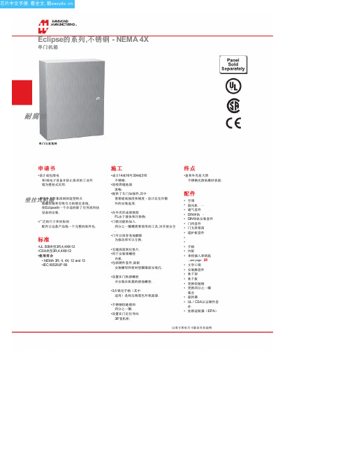
Eclipse的系列,不锈钢 - NEMA 4X
单门机箱
304 S.S.
零件号
EN4SD12126SS EN4SD16126SS EN4SD16166SS EN4SD16206SS EN4SD20166SS EN4SD20206SS EN4SD24206SS EN4SD16128SS EN4SD16168SS
外形尺寸
Door/
车身闭锁
A B C Gauge Qty
12.00 12.00 6.00 16
1
16.00 12.00 6.00 16
1
16.00 16.00 6.00 16
1
16.00 20.00 6.00 16
1
20.00 16.00 6.00 16
1
20.00 20.00 6.00 16
1
24.00 20.00 6.00 16
EN4SD30248S16 EN4SD30308S16 EN4SD36248S16 EN4SD36308S16 EN4SD161210S16 EN4SD161610S16 EN4SD162010S16 EN4SD201610S16 EN4SD202010S16 EN4SD202410S16 EN4SD241610S16 EN4SD242010S16 EN4SD242410S16 EN4SD243010S16 EN4SD302010S16 EN4SD302410S16 EN4SD303010S16 EN4SD362410S16 EN4SD363010S16 EN4SD482410S16 EN4SD202012S16 EN4SD242412S16 EN4SD302412S16 EN4SD362412S16 EN4SD363012S16 EN4SD363612S16 EN4SD483616S16R
MEMORY存储芯片MT41K512M16TNA-107 E中文规格书
Post Package RepairPost Package RepairJEDEC defines two modes of Post Package Repair (PPR): soft Post Package Repair (sPPR)and hard Post Package Repair (hPPR). sPPR is non-persistent so the repair row maybe altered; that is, sPPR is NOT a permanent repair and even though it will repair a row, the repair can be reversed, reassigned via another sPPR, or made permanent via hPPR.Hard Post Package Repair is persistent so once the repair row is assigned for a hPPR ad-dress, further PPR commands to a previous hPPR section should not be performed, that is, hPPR is a permanent repair; once repaired, it cannot be reversed. The controller pro-vides the failing row address in the hPPR/sPPR sequence to the device to perform the row repair. hPPR Mode and sPPR Mode may not be enabled at the same time.JEDEC states hPPR is optional for 4Gb and sPPR is optional for 4Gb and 8Gb parts how-ever Micron 4Gb and 8Gb DDR4 DRAMs should have both sPPR and hPPR support. The hPPR support is identified via an MPR read from MPR Page 2, MPR0[7] and sPPR sup-port is identified via an MPR read from MPR Page 2, MPR0[6].The JEDEC minimum support requirement for DDR4 PPR (hPPR or sPPR) is to provide one row of repair per bank group (BG), x4/x8 have 4 BG and x16 has 2 BG; this is a total of 4 repair rows available on x4/x8 and 2 repair rows available on x16. Micron PPR sup-port exceeds the JEDEC minimum requirements; Micron DDR4 DRAMs have at least one row of repair for each bank which is essentially 4 row repairs per BG for a total of 16repair rows for x4 and x8 and 8 repair rows for x16; a 4x increase in repair rows.JEDEC requires the user to have all sPPR row repair addresses reset and cleared prior to enabling hPPR Mode. Micron DDR4 PPR does not have this restriction, the existing sPPR row repair addresses are not required to be cleared prior to entering hPPR mode.Each bank in a BG is PPR independent: sPPR or hPPR issued to a bank will not alter a sPPR row repair existing in a different bank.sPPR followed by sPPR to same bankWhen PPR is issued to a bank for the first time and is a sPPR command, the repair row will be a sPPR. When a subsequent sPPR is issued to the same bank, the previous sPPR repair row will be cleared and used for the subsequent sPPR address as the sPPR opera-tion is non-persistent.sPPR followed by hPPR to same bankWhen a PPR is issued to a bank for the first time and is a sPPR command, the repair row will be a sPPR. When a subsequent hPPR is issued to the same bank, the initial sPPR repair row will be cleared and used for the hPPR address. If a further subsequent PPR (hPPR or sPPR) is issued to the same bank, the further subsequent PPR ( hPPR or sPPR)repair row will not clear or overwrite the previous hPPR address as the hPPR operation is persistent.hPPR followed by hPPR or sPPR to same bankWhen a PPR is issued to a bank for the first time and is a hPPR command, the repair row will be a hPPR. When a subsequent PPR (hPPR or sPPR) is issued to the same bank, the subsequent PPR ( hPPR or sPPR) repair row will not clear or overwrite the initial hPPR address as the initial hPPR is persistent.8Gb: x8, x16 Automotive DDR4 SDRAM Post Package Repairvalue may not be exactly within the voltage range setting coupled with the V REF set tol-erance; the device must be calibrated to the correct internal V REFDQ voltage.Figure 62: Example of V REF Set Tolerance and Step SizeV REFDigital CodeNote: 1.Maximum case shown.V REFDQ Increment and Decrement TimingThe V REF increment/decrement step times are defined by V REF ,time . V REF ,time is defined from t0 to t1, where t1 is referenced to the V REF voltage at the final DC level within the V REF valid tolerance (V REF ,val_tol ). The V REF valid level is defined by V REF ,val tolerance to qualify the step time t1. This parameter is used to insure an adequate RC time constant behavior of the voltage level change after any V REF increment/decrement adjustment.8Gb: x8, x16 Automotive DDR4 SDRAM V REFDQ Calibration。
MEMORY存储芯片MT48LC4M16A2TG-75L G中文规格书
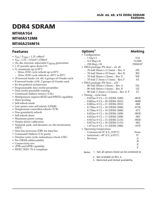
DDR4 SDRAM MT40A1G4MT40A512M8MT40A256M16Features•V DD = V DDQ = 1.2V ±60mV•V PP = 2.5V, –125mV/+250mV•On-die, internal, adjustable V REFDQ generation •1.2V pseudo open-drain I/O•T C maximum up to 95°C–64ms, 8192-cycle refresh up to 85°C–32ms, 8192-cycle refresh at >85°C to 95°C•16 internal banks (x4, x8): 4 groups of 4 banks each •8 internal banks (x16): 2 groups of 4 banks each •8n-bit prefetch architecture•Programmable data strobe preambles•Data strobe preamble training•Command/Address latency (CAL)•Multipurpose register READ and WRITE capability •Write leveling•Self refresh mode•Low-power auto self refresh (LPASR)•Temperature controlled refresh (TCR)•Fine granularity refresh•Self refresh abort•Maximum power saving•Output driver calibration•Nominal, park, and dynamic on-die termination (ODT)•Data bus inversion (DBI) for data bus •Command/Address (CA) parity•Databus write cyclic redundancy check (CRC)•Per-DRAM addressability•Connectivity test•sPPR and hPPR capability•JEDEC JESD-79-4 compliant Options1Marking •Configuration– 1 Gig x 41G4–512 Meg x 8512M8–256 Meg x 16256M162•FBGA package (Pb-free) – x4, x8–78-ball (9mm x 11.5mm) – Rev. A HX–78-ball (9mm x 10.5mm) – Rev. B RH–78-ball (8mm x 12mm) – Rev. E WE–78-ball (7.5mm x 11mm) – Rev. F SA •FBGA package (Pb-free) – x16–96-ball (9mm x 14mm) – Rev. A HA–96-ball (9mm x 14mm) – Rev. B GE–96-ball (7.5mm x 13.5mm) – Rev. E, F LY •Timing – cycle time–0.625ns @ CL = 22 (DDR4-3200)-062E–0.682ns @ CL = 20 (DDR4-2933)-068E–0.682ns @ CL = 21 (DDR4-2933)-068–0.750ns @ CL = 18 (DDR4-2666)-075E–0.750ns @ CL = 19 (DDR4-2666)-075–0.833ns @ CL = 16 (DDR4-2400)-083E–0.833ns @ CL = 17 (DDR4-2400)-083–0.937ns @ CL = 15 (DDR4-2133)-093E–0.937ns @ CL = 16 (DDR4-2133)-093– 1.071ns @ CL = 13 (DDR4-1866)-107E •Operating temperature–Commercial (0° ื T Cื 95°C)None–Industrial (–40° ื T Cื 95°C)IT–Revision:A:B:E:F Notes: 1.Not all options listed can be combined to2.Not available on Rev. A.3.Restricted and limited availability.Burst Length, Type, and OrderAccesses within a given burst may be programmed to sequential or interleaved order.The ordering of accesses within a burst is determined by the burst length, burst type,and the starting column address as shown in the following table. Burst length optionsinclude fixed BC4, fixed BL8, and on-the-fly (OTF), which allows BC4 or BL8 to be selec-ted coincidentally with the registration of a READ or WRITE command via A12/BC_n. Table 8: Burst Type and Burst OrderNotes: 1.0...7 bit number is the value of CA[2:0] that causes this bit to be the first read during aburst.2.When setting burst length to BC4 (fixed) in MR0, the internal WRITE operation startstwo clock cycles earlier than for the BL8 mode, meaning the starting point for t WR andt WTR will be pulled in by two clocks. When setting burst length to OTF in MR0, the in-ternal WRITE operation starts at the same time as a BL8 (even if BC4 was selected duringcolumn time using A12/BC4_n) meaning that if the OTF MR0 setting is used, the startingpoint for t WR and t WTR will not be pulled in by two clocks as described in the BC4(fixed) case.3.T = Output driver for data and strobes are in High-Z.V = Valid logic level (0 or 1), but respective buffer input ignores level on input pins.X = “Don’t Care.”。
54LS02E中文资料
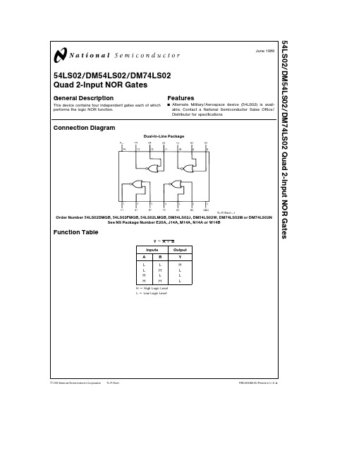
TL F 644154LS02 DM54LS02 DM74LS02 Quad 2-Input NOR GatesJune1989 54LS02 DM54LS02 DM74LS02Quad2-Input NOR GatesGeneral DescriptionThis device contains four independent gates each of whichperforms the logic NOR functionFeaturesY Alternate Military Aerospace device(54LS02)is avail-able Contact a National Semiconductor Sales OfficeDistributor for specificationsConnection DiagramDual-In-Line PackageTL F 6441–1 Order Number54LS02DMQB 54LS02FMQB 54LS02LMQB DM54LS02J DM54LS02W DM74LS02M or DM74LS02NSee NS Package Number E20A J14A M14A N14A or W14BFunction TableY e A a BInputs OutputA B YL L HL H LH L LH H LH e High Logic LevelL e Low Logic LevelC1995National Semiconductor Corporation RRD-B30M105 Printed in U S AAbsolute Maximum Ratings(Note)If Military Aerospace specified devices are required please contact the National Semiconductor Sales Office Distributors for availability and specifications Supply Voltage7V Input Voltage7V Operating Free Air Temperature RangeDM54LS and54LS b55 C to a125 C DM74LS0 C to a70 C Storage Temperature Range b65 C to a150 C Note The‘‘Absolute Maximum Ratings’’are those values beyond which the safety of the device cannot be guaran-teed The device should not be operated at these limits The parametric values defined in the‘‘Electrical Characteristics’’table are not guaranteed at the absolute maximum ratings The‘‘Recommended Operating Conditions’’table will define the conditions for actual device operationRecommended Operating ConditionsSymbol ParameterDM54LS02DM74LS02Units Min Nom Max Min Nom MaxV CC Supply Voltage4 555 54 7555 25V V IH High Level Input Voltage22V V IL Low Level Input Voltage0 70 8V I OH High Level Output Current b0 4b0 4mA I OL Low Level Output Current48mA T A Free Air Operating Temperature b55125070 CElectrical Characteristics over recommended operating free air temperature range(unless otherwise noted)Symbol Parameter Conditions MinTypMax Units (Note1)V I Input Clamp Voltage V CC e Min I I e b18mA b1 5V V OH High Level Output V CC e Min I OH e Max DM542 53 4V Voltage V IL e Max DM742 73 4V OL Low Level Output V CC e Min I OL e Max DM540 250 4 Voltage V IH e Min DM740 350 5VI OL e4mA V CC e Min DM740 250 4I I Input Current Max V CC e Max V I e7V0 1mAInput VoltageI IH High Level Input Current V CC e Max V I e2 7V20m A I IL Low Level Input Current V CC e Max V I e0 4V b0 40mAI OS Short Circuit V CC e Max DM54b20b100mA Output Current(Note2)DM74b20b100I CCH Supply Current with V CC e Max1 63 2mAOutputs HighI CCL Supply Current with V CC e Max2 85 4mAOutputs LowSwitching Characteristics at V CC e5V and T A e25 C(See Section1for Test Waveforms and Output Load)R L e2k XSymbol Parameter C L e15pF C L e50pF UnitsMin Max Min Maxt PLH Propagation Delay Time1318ns Low to High Level Outputt PHL Propagation Delay Time1015ns High to Low Level OutputNote1 All typicals are at V CC e5V T A e25 CNote2 Not more than one output should be shorted at a time and the duration should not exceed one second2Physical Dimensions inches(millimeters)Ceramic Leadless Chip Carrier Package(E)Order Number54LS02LMQBNS Package Number E20A3Physical Dimensions inches(millimeters)(Continued)14-Lead Ceramic Dual-In-Line Package(J)Order Number54LS02DMQB or DM54LS02JNS Package Number J14A14-Lead Small Outline Molded Package(M)Order Number DM74LS02MNS Package Number M14A4Physical Dimensions inches(millimeters)(Continued)14-Lead Molded Dual-In-Line Package(N)Order Number DM74LS02NNS Package Number N14A554L S 02 D M 54L S 02 D M 74L S 02Q u a d 2-I n p u t N O R G a t e sPhysical Dimensions inches (millimeters)(Continued)14-Lead Ceramic Flat Package (W)Order Number 54LS02FMQB or DM54LS02WNS Package Number W14BLIFE SUPPORT POLICYNATIONAL’S PRODUCTS ARE NOT AUTHORIZED FOR USE AS CRITICAL COMPONENTS IN LIFE SUPPORT DEVICES OR SYSTEMS WITHOUT THE EXPRESS WRITTEN APPROVAL OF THE PRESIDENT OF NATIONAL SEMICONDUCTOR CORPORATION As used herein 1 Life support devices or systems are devices or 2 A critical component is any component of a life systems which (a)are intended for surgical implant support device or system whose failure to perform can into the body or (b)support or sustain life and whose be reasonably expected to cause the failure of the life failure to perform when properly used in accordance support device or system or to affect its safety or with instructions for use provided in the labeling can effectivenessbe reasonably expected to result in a significant injury to the userNational Semiconductor National Semiconductor National Semiconductor National Semiconductor CorporationEuropeHong Kong LtdJapan Ltd1111West Bardin RoadFax (a 49)0-180-530858613th Floor Straight Block Tel 81-043-299-2309。
- 1、下载文档前请自行甄别文档内容的完整性,平台不提供额外的编辑、内容补充、找答案等附加服务。
- 2、"仅部分预览"的文档,不可在线预览部分如存在完整性等问题,可反馈申请退款(可完整预览的文档不适用该条件!)。
- 3、如文档侵犯您的权益,请联系客服反馈,我们会尽快为您处理(人工客服工作时间:9:00-18:30)。
E
C
Product Code
K
D
Style
4
A
1
0
2
M
Cap. Tol.
D
Temp. Char.
U
Suffix
(Examples)
Rated Voltage
Nominal Capacitance
s Specifications
Characteristics Operating Temperature Range Rated Voltage Dielectric Withstanding VoltageV Capacitance Dissipation Factor (tan d) Insulation Resistance Temperature Characteristics Specifications Ð25 to 85 ûC 4 kVDC to 15 kVDC 150 % of the rated voltage for 1 to 5 seconds Within tolerance, when measured at 1 kHz±20 %, 1 to 5 Vrms, and 20 ûC 0.025 max. at 1 kHz±20 %, 1 to 5 Vrms, and 20 ûC 10000 MΩ min. at 500 VDC and 1 minute electrification Capacitance Change: +20, Ð30 % max. over the temperature range of Ð25 to 85 ûC
s Precautions for Handling
See Page 84 to 86
Hale Waihona Puke s Packaging Informations
See Page 87 to 88
V Dielectric Withstanding Voltage test for the rated voltage of 6 kVDC and above shall be conducted in insulating oil.
Design and Specifications are subject to change without notice. Ask factory for technical specifications before purchase and/or use. Whenever a doubt about safety issues arises from this product, please inform us immediately for technical consultation.
s Recommended Applications
q High voltage power supply q High voltage circuit of TV and CRT display q High voltage DC circuit
s Explanation of Part Numbers
4 kVDC
6 kVDC
8 kVDC
10 kVDC
15 kVDC
Design and Specifications are subject to change without notice. Ask factory for technical specifications before purchase and/or use. Whenever a doubt about safety issues arises from this product, please inform us immediately for technical consultation.
元器件交易网
Ceramic Disc Capacitors (High Voltage)
s Dimensions in mm (not to scale) s Typical Temperature Characteristics
+ +
s Ratings and Characteristics
元器件交易网
Ceramic Disc Capacitors (High Voltage)
High Voltage Ceramic Disc Capacitors, Rated 4 to 15 kVDC, Temp. Char. Y5T
Series:
MDU
s Features
Rated Voltage Part Number ECKD3G101MDU ECKD3G151MDU ECKD3G221MDU ECKD3G331MDU ECKD3G471MDU ECKD3G681MDU ECKD3G102MDU ECKD3G152MDU ECKD3G222MDU ECKD3J101MDU ECKD3J151MDU ECKD3J221MDU ECKD3J331MDU ECKD3J471MDU ECKD3J681MDU ECKD3J102MDU ECKD3J152MDU ECKD3J222MDU ECKD3K101MDU ECKD3K151MDU ECKD3K221MDU ECKD3K331MDU ECKD3K471MDU ECKD3K681MDU ECKD3K102MDU ECKD3K152MDU ECKD4A101MDU ECKD4A151MDU ECKD4A221MDU ECKD4A331MDU ECKD4A471MDU ECKD4A681MDU ECKD4A102MDU ECKD4C101MDU ECKD4C151MDU ECKD4C221MDU ECKD4C331MDU ECKD4C471MDU ECKD4C681MDU ECKD4C102MDU Capacitance Nominal Cap. Tolerance (pF) (%) 100 150 220 330 470 680 1000 1500 2200 100 150 220 330 470 680 1000 1500 2200 100 150 220 330 470 680 1000 1500 100 150 220 330 470 680 1000 100 150 220 330 470 680 1000 ±20 ±20 ±20 ±20 ±20 ±20 ±20 ±20 ±20 ±20 ±20 ±20 ±20 ±20 ±20 ±20 ±20 ±20 ±20 ±20 ±20 ±20 ±20 ±20 ±20 ±20 ±20 ±20 ±20 ±20 ±20 ±20 ±20 ±20 ±20 ±20 ±20 ±20 ±20 ±20 Dimensions in mm D max. 7.0 7.0 7.0 8.0 8.5 9.5 11.5 13.5 16.0 8.0 8.0 8.0 10.5 11.5 13.0 15.0 17.5 21.5 8.0 8.0 8.5 10.0 11.5 13.5 16.5 18.5 8.0 8.5 9.5 11.5 13.0 15.0 16.5 8.0 9.0 10.0 11.5 13.5 15.0 19.0 T max. 7.0 7.0 7.0 7.0 7.0 7.0 7.0 7.0 7.0 8.0 8.0 8.0 8.0 8.0 8.0 8.0 8.0 8.0 9.0 9.0 9.0 9.0 9.0 9.0 9.0 9.0 9.0 9.0 9.0 9.0 9.0 9.0 9.0 10.0 10.0 10.0 10.0 10.0 10.0 10.0 F 7.5±2.0 7.5±2.0 7.5±2.0 7.5±2.0 7.5±2.0 10.0±2.0 10.0±2.0 10.0±2.0 10.0±2.0 10.0±2.0 10.0±2.0 10.0±2.0 10.0±2.0 10.0±2.0 10.0±2.0 10.0±2.0 10.0±2.0 10.0±2.0 10.0±2.0 10.0±2.0 10.0±2.0 10.0±2.0 10.0±2.0 10.0±2.0 10.0±2.0 10.0±2.0 10.0±2.0 10.0±2.0 10.0±2.0 10.0±2.0 10.0±2.0 10.0±2.0 10.0±2.0 10.0±2.0 10.0±2.0 10.0±2.0 10.0±2.0 10.0±2.0 12.5±2.0 12.5±2.0 d 0.65 0.65 0.65 0.65 0.65 0.65 0.65 0.65 0.65 0.65 0.65 0.65 0.80 0.80 0.80 0.80 0.80 0.80 0.65 0.65 0.65 0.65 0.80 0.80 0.80 0.80 0.65 0.65 0.65 0.80 0.80 0.80 0.80 0.65 0.65 0.65 0.80 0.80 0.80 0.80
q Wide products range of 4 to 15 kVDC q Voltage stable type dielectric materials applied for high voltage application q Flame-retardant insulating coating applied