SN54HC573A PDF资料
54FCT573LMQB资料
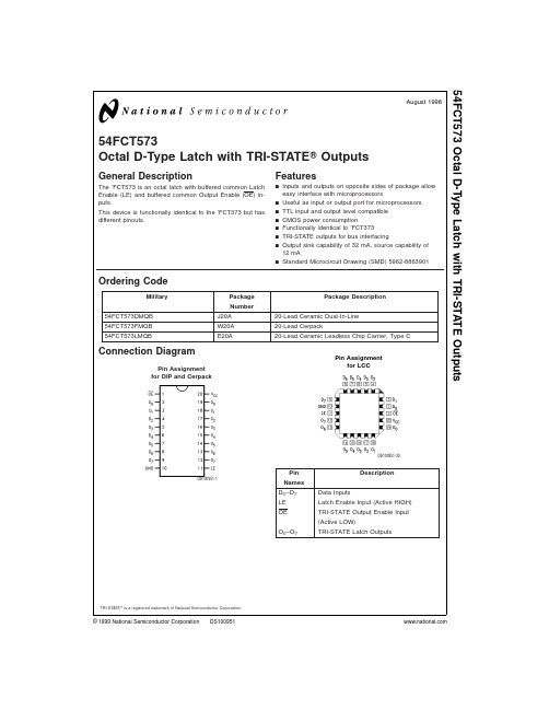
54FCT573Octal D-Type Latch with TRI-STATE ®OutputsGeneral DescriptionThe ’FCT573is an octal latch with buffered common Latch Enable (LE)and buffered common Output Enable (OE)in-puts.This device is functionally identical to the ’FCT373but has different pinouts.Featuresn Inputs and outputs on opposite sides of package allow easy interface with microprocessorsn Useful as input or output port for microprocessors n TTL input and output level compatible n CMOS power consumptionn Functionally identical to ’FCT373n TRI-STATE outputs for bus interfacingn Output sink capability of 32mA,source capability of 12mAn Standard Microcircuit Drawing (SMD)5962-8863901Ordering CodeMilitaryPackage Package DescriptionNumber 54FCT573DMQB J20A 20-Lead Ceramic Dual-In-Line 54FCT573FMQB W20A 20-Lead Cerpack54FCT573LMQBE20A20-Lead Ceramic Leadless Chip Carrier,Type CConnection DiagramPin Names DescriptionD 0–D 7Data InputsLE Latch Enable Input (Active HIGH)OE TRI-STATE Output Enable Input (Active LOW)O 0–O 7TRI-STATE Latch OutputsTRI-STATE ®is a registered trademark of National Semiconductor Corporation.Pin Assignment for DIP and CerpackDS100951-1Pin Assignmentfor LCC DS100951-39August 199854FCT573Octal D-Type Latch with TRI-STATE Outputs©1999National Semiconductor Corporation Functional DescriptionThe ’FCT573contains eight D-type latches with TRI-STATE output buffers.When the Latch Enable (LE)input is HIGH,data on the D n inputs enters the latches.In this condition the latches are transparent,i.e.,a latch output will change state each time its D input changes.When LE is LOW the latches store the information that was present on the D inputs a setup time preceding the HIGH-to-LOW transition of LE.The TRI-STATE buffers are controlled by the Output Enable (OE)input.When OE is LOW,the buffers are in the bi-state mode.When OE is HIGH the buffers are in the high impedance mode but this does not interfere with entering new data into the latches.Function Table Inputs OutputsOE LED O L H H H L H L L L L X O 0HXXZH =HIGH Voltage Level L =LOW Voltage Level X =ImmaterialO 0=Value stored from previous clock cycleLogic DiagramDS100951-3Please note that this diagram is provided only for the understanding of logic operations and should not be used to estimate propagation delays.54F C T 573 2Absolute Maximum Ratings(Note1)If Military/Aerospace specified devices are required, please contact the National Semiconductor Sales Office/ Distributors for availability and specifications.Storage Temperature−65˚C to+150˚C Ambient Temperature under Bias−55˚C to+125˚C Junction Temperature under BiasCeramic−55˚C to+175˚C V CC Pin Potential toGround Pin−0.5V to+7.0V Input Voltage(Note2)−0.5V to+7.0V Input Current(Note2)−30mA to+5.0mA Voltage Applied to Any Outputin the Disabled orPower-Off State−0.5V to+5.5V in the HIGH State−0.5V to V CC Current Applied to Outputin LOW State(Max)Twice the rated I OL(mA) DC Latchup Source Current−500mARecommended Operating ConditionsFree Air Ambient TemperatureMilitary−55˚C to+125˚C Supply VoltageMilitary+4.5V to+5.5V Minimum Input Edge Rate(∆V/∆t) Data Input50mV/ns Enable Input20mV/ns Note1:Absolute maximum ratings are values beyond which the device may be damaged or have its useful life impaired.Functional operation under these conditions is not implied.Note2:Either voltage limit or current limit is sufficient to protect inputs.DC Electrical CharacteristicsSymbol Parameter FCT573Units V CC ConditionsMin Typ MaxV IH Input HIGH Voltage 2.0V Recognized HIGH Signal V IL Input LOW Voltage0.8V Recognized LOW Signal V CD Input Clamp Diode Voltage−1.2V Min I IN=−18mAV OH Output HIGHVoltage 54FCT 4.3V MinI OH=−300µA 54FCT 2.4I OH=−12mAV OL Output LOWVoltage54FCT0.2V Min I OL=300µA54FCT0.5I OL=32mAI IH Input HIGH Current5µA Max V IN=V CCI IL Input LOW Current−5µA Max V IN=0.0VI OZH Output Leakage Current50µA0−5.5VV OUT=2.7V;OE=2.0VI OZL Output Leakage Current−50µA0−5.5VV OUT=0.5V;OE=2.0VI OS Output Short-Circuit Current-60mA Max V OUT=0.0VI CCQ Quiescent Power Supply Current 1.5mA Max V IN<0.2V or V IN5.3V,V CC=5.5V∆I CC Quiescent PowerSupply Current2.0mA Max V I=3.4V,V CC=5.5VI CCD Dynamic I CC0.4mA/MHz Max Outputs Open,V CC=5.5V,V IN5.3V or V IN<0.2V,One BitToggling,50%Duty Cycle,OE=GND,LE=V CCI CC Total Power SupplyCurrent6.0mA Max Outputs Open,f CP=10MHz,V CC=5.5V,V IN5.3V or V IN<0.2V,One Bit Toggling,50%Duty Cycle,OE=GND,LE=V CC54FCT5733AC Electrical CharacteristicsSymbolParameter54FCTUnitsFig.No.T A =−55˚C to +125˚C V CC =4.5V to 5.5VC L =50pFMinMax t PLH Propagation Delay 1.08.5ns Figure 4t PHL D n to O n1.08.5t PLH Propagation Delay 1.015.0ns Figure 4t PHL LE to O n1.015.0t PZH Output Enable Time1.013.5ns Figure 6t PZL 1.013.5t PHZ Output Disable Time 1.010.0ns Figure 6t PLZTime1.010.0AC Operating RequirementsSymbolParameter54FCTUnitsFig.No.T A =−55˚C to +125˚C V CC =4.5V to 5.5VC L =50pFMinMaxt s (H)Set Time,HIGH 2.0ns Figure 7t s (L)or LOW D n to LE 2.0t h (H)Hold Time,HIGH 1.5nsFigure 7t h (L)or LOW D n to LE 1.5t w (H)Pulse Width, 6.0ns Figure 5LE HIGHCapacitanceSymbol Parameter Max Units Conditions (T A =25˚C)C INInput Capacitance 10pF V CC =0V C OUT (Note 3)Output Capacitance12pFV CC =5.0VNote 3:C OUT is measured at frequency f =1MHz per MIL-STD-883B,Method 3012.54F C T 573 4AC LoadingDS100951-4 *Includes jig and probe capacitanceFIGURE1.Test LoadDS100951-6 FIGURE2.Test Input Signal LevelsAmplitude Rep.Rate t w t r t f3.0V1MHz500ns 2.5ns 2.5nsFIGURE3.Test Input Signal RequirementsDS100951-8 FIGURE4.Propagation Delay Waveforms for Inverting and Non-Inverting FunctionsDS100951-5FIGURE5.Propagation Delay,Pulse Width WaveformsDS100951-7FIGURE6.TRI-STATE Output HIGHand LOW Enable and Disable TimesDS100951-9FIGURE7.Setup Time,Hold Timeand Recovery Time Waveforms54FCT5735Physical Dimensionsinches (millimeters)unless otherwise noted20-Lead Ceramic Leadless Chip CarrierNS Package Number E20A20-Lead Ceramic Dual-In-Line NS Package Number J20A54F C T 5736Physical Dimensions inches(millimeters)unless otherwise noted(Continued)LIFE SUPPORT POLICYNATIONAL’S PRODUCTS ARE NOT AUTHORIZED FOR USE AS CRITICAL COMPONENTS IN LIFE SUPPORT DEVICES OR SYSTEMS WITHOUT THE EXPRESS WRITTEN APPROVAL OF THE PRESIDENT AND GENERAL COUNSEL OF NATIONAL SEMICONDUCTOR CORPORATION.As used herein:1.Life support devices or systems are devices orsystems which,(a)are intended for surgical implantinto the body,or(b)support or sustain life,andwhose failure to perform when properly used inaccordance with instructions for use provided in thelabeling,can be reasonably expected to result in asignificant injury to the user.2.A critical component is any component of a lifesupport device or system whose failure to performcan be reasonably expected to cause the failure ofthe life support device or system,or to affect itssafety or effectiveness.National SemiconductorCorporationAmericasTel:1-800-272-9959Fax:1-800-737-7018Email:support@National SemiconductorEuropeFax:+49(0)180-5308586Email:europe.support@Deutsch Tel:+49(0)180-5308585English Tel:+49(0)180-5327832Français Tel:+49(0)180-5329358Italiano Tel:+49(0)180-5341680National SemiconductorAsia Pacific CustomerResponse GroupTel:65-2544466Fax:65-2504466Email:sea.support@National SemiconductorJapan Ltd.Tel:81-3-5639-7560Fax:81-3-5639-7507 20-Lead Ceramic FlatpackNS Package Number W20A54FCT573OctalD-TypeLatchwithTRI-STATEOutputs National does not assume any responsibility for use of any circuitry described,no circuit patent licenses are implied and National reserves the right at any time without notice to change said circuitry and specifications.。
SN54HC373中文资料

元器件交易网IMPORTANT NOTICETexas Instruments and its subsidiaries (TI) reserve the right to make changes to their products or to discontinueany product or service without notice, and advise customers to obtain the latest version of relevant informationto verify, before placing orders, that information being relied on is current and complete. All products are soldsubject to the terms and conditions of sale supplied at the time of order acknowledgement, including thosepertaining to warranty, patent infringement, and limitation of liability.TI warrants performance of its semiconductor products to the specifications applicable at the time of sale inaccordance with TI’s standard warranty. Testing and other quality control techniques are utilized to the extentTI deems necessary to support this warranty. Specific testing of all parameters of each device is not necessarilyperformed, except those mandated by government requirements.CERTAIN APPLICATIONS USING SEMICONDUCTOR PRODUCTS MAY INVOLVE POTENTIAL RISKS OFDEATH, PERSONAL INJURY, OR SEVERE PROPERTY OR ENVIRONMENTAL DAMAGE (“CRITICALAPPLICATIONS”). TI SEMICONDUCTOR PRODUCTS ARE NOT DESIGNED, AUTHORIZED, ORWARRANTED TO BE SUITABLE FOR USE IN LIFE-SUPPORT DEVICES OR SYSTEMS OR OTHERCRITICAL APPLICATIONS. INCLUSION OF TI PRODUCTS IN SUCH APPLICATIONS IS UNDERSTOOD TOBE FULLY AT THE CUSTOMER’S RISK.In order to minimize risks associated with the customer’s applications, adequate design and operatingsafeguards must be provided by the customer to minimize inherent or procedural hazards.TI assumes no liability for applications assistance or customer product design. TI does not warrant or representthat any license, either express or implied, is granted under any patent right, copyright, mask work right, or otherintellectual property right of TI covering or relating to any combination, machine, or process in which suchsemiconductor products or services might be or are used. TI’s publication of information regarding any thirdparty’s products or services does not constitute TI’s approval, warranty or endorsement thereof.Copyright © 1998, Texas Instruments Incorporated。
SN74LVC573A中文资料

元器件交易网IMPORTANT NOTICETexas Instruments and its subsidiaries (TI) reserve the right to make changes to their products or to discontinueany product or service without notice, and advise customers to obtain the latest version of relevant informationto verify, before placing orders, that information being relied on is current and complete. All products are soldsubject to the terms and conditions of sale supplied at the time of order acknowledgement, including thosepertaining to warranty, patent infringement, and limitation of liability.TI warrants performance of its semiconductor products to the specifications applicable at the time of sale inaccordance with TI’s standard warranty. Testing and other quality control techniques are utilized to the extentTI deems necessary to support this warranty. Specific testing of all parameters of each device is not necessarilyperformed, except those mandated by government requirements.CERTAIN APPLICATIONS USING SEMICONDUCTOR PRODUCTS MAY INVOLVE POTENTIAL RISKS OFDEATH, PERSONAL INJURY, OR SEVERE PROPERTY OR ENVIRONMENTAL DAMAGE (“CRITICALAPPLICATIONS”). TI SEMICONDUCTOR PRODUCTS ARE NOT DESIGNED, AUTHORIZED, ORWARRANTED TO BE SUITABLE FOR USE IN LIFE-SUPPORT DEVICES OR SYSTEMS OR OTHERCRITICAL APPLICATIONS. INCLUSION OF TI PRODUCTS IN SUCH APPLICATIONS IS UNDERSTOOD TOBE FULLY AT THE CUSTOMER’S RISK.In order to minimize risks associated with the customer’s applications, adequate design and operatingsafeguards must be provided by the customer to minimize inherent or procedural hazards.TI assumes no liability for applications assistance or customer product design. TI does not warrant or representthat any license, either express or implied, is granted under any patent right, copyright, mask work right, or otherintellectual property right of TI covering or relating to any combination, machine, or process in which suchsemiconductor products or services might be or are used. TI’s publication of information regarding any thirdparty’s products or services does not constitute TI’s approval, warranty or endorsement thereof.Copyright © 1998, Texas Instruments Incorporated。
SN74HC573ANE4中文资料

PACKAGING INFORMATIONOrderable Device Status(1)PackageType PackageDrawingPins PackageQtyEco Plan(2)Lead/Ball Finish MSL Peak Temp(3)5962-8512801VRA ACTIVE CDIP J201TBD A42SNPB N/A for Pkg Type 5962-8512801VSA ACTIVE CFP W201TBD A42N/A for Pkg Type 85128012A ACTIVE LCCC FK201TBD POST-PLATE N/A for Pkg Type 8512801RA ACTIVE CDIP J201TBD A42SNPB N/A for Pkg Type 8512801SA ACTIVE CFP W201TBD A42N/A for Pkg Type JM38510/65406BRA ACTIVE CDIP J201TBD A42SNPB N/A for Pkg Type SN54HC573AJ ACTIVE CDIP J201TBD A42SNPB N/A for Pkg Type SN74HC573ADBR ACTIVE SSOP DB202000Green(RoHS&no Sb/Br)CU NIPDAU Level-1-260C-UNLIMSN74HC573ADBRE4ACTIVE SSOP DB202000Green(RoHS&no Sb/Br)CU NIPDAU Level-1-260C-UNLIMSN74HC573ADBRG4ACTIVE SSOP DB202000Green(RoHS&no Sb/Br)CU NIPDAU Level-1-260C-UNLIMSN74HC573ADW ACTIVE SOIC DW2025Green(RoHS&no Sb/Br)CU NIPDAU Level-1-260C-UNLIMSN74HC573ADWE4ACTIVE SOIC DW2025Green(RoHS&no Sb/Br)CU NIPDAU Level-1-260C-UNLIMSN74HC573ADWG4ACTIVE SOIC DW2025Green(RoHS&no Sb/Br)CU NIPDAU Level-1-260C-UNLIMSN74HC573ADWR ACTIVE SOIC DW202000Green(RoHS&no Sb/Br)CU NIPDAU Level-1-260C-UNLIMSN74HC573ADWRE4ACTIVE SOIC DW202000Green(RoHS&no Sb/Br)CU NIPDAU Level-1-260C-UNLIMSN74HC573ADWRG4ACTIVE SOIC DW202000Green(RoHS&no Sb/Br)CU NIPDAU Level-1-260C-UNLIMSN74HC573AN ACTIVE PDIP N2020Pb-Free(RoHS)CU NIPDAU N/A for Pkg Type SN74HC573AN3OBSOLETE PDIP N20TBD Call TI Call TISN74HC573ANE4ACTIVE PDIP N2020Pb-Free(RoHS)CU NIPDAU N/A for Pkg Type SN74HC573APWLE OBSOLETE TSSOP PW20TBD Call TI Call TISN74HC573APWR ACTIVE TSSOP PW202000Green(RoHS&no Sb/Br)CU NIPDAU Level-1-260C-UNLIMSN74HC573APWRE4ACTIVE TSSOP PW202000Green(RoHS&no Sb/Br)CU NIPDAU Level-1-260C-UNLIMSN74HC573APWRG4ACTIVE TSSOP PW202000Green(RoHS&no Sb/Br)CU NIPDAU Level-1-260C-UNLIMSN74HC573APWT ACTIVE TSSOP PW20250Green(RoHS&no Sb/Br)CU NIPDAU Level-1-260C-UNLIMSN74HC573APWTE4ACTIVE TSSOP PW20250Green(RoHS&no Sb/Br)CU NIPDAU Level-1-260C-UNLIMSN74HC573APWTG4ACTIVE TSSOP PW20250Green(RoHS&no Sb/Br)CU NIPDAU Level-1-260C-UNLIM SNJ54HC573AFK ACTIVE LCCC FK201TBD POST-PLATE N/A for Pkg Type SNJ54HC573AJ ACTIVE CDIP J201TBD A42SNPB N/A for Pkg Type SNJ54HC573AW ACTIVE CFP W201TBD A42N/A for Pkg Type (1)The marketing status values are defined as follows:24-Sep-2007ACTIVE:Product device recommended for new designs.LIFEBUY:TI has announced that the device will be discontinued,and a lifetime-buy period is in effect.NRND:Not recommended for new designs.Device is in production to support existing customers,but TI does not recommend using this part in a new design.PREVIEW:Device has been announced but is not in production.Samples may or may not be available.OBSOLETE:TI has discontinued the production of the device.(2)Eco Plan -The planned eco-friendly classification:Pb-Free (RoHS),Pb-Free (RoHS Exempt),or Green (RoHS &no Sb/Br)-please check /productcontent for the latest availability information and additional product content details.TBD:The Pb-Free/Green conversion plan has not been defined.Pb-Free (RoHS):TI's terms "Lead-Free"or "Pb-Free"mean semiconductor products that are compatible with the current RoHS requirements for all 6substances,including the requirement that lead not exceed 0.1%by weight in homogeneous materials.Where designed to be soldered at high temperatures,TI Pb-Free products are suitable for use in specified lead-free processes.Pb-Free (RoHS Exempt):This component has a RoHS exemption for either 1)lead-based flip-chip solder bumps used between the die and package,or 2)lead-based die adhesive used between the die and leadframe.The component is otherwise considered Pb-Free (RoHS compatible)as defined above.Green (RoHS &no Sb/Br):TI defines "Green"to mean Pb-Free (RoHS compatible),and free of Bromine (Br)and Antimony (Sb)based flame retardants (Br or Sb do not exceed 0.1%by weight in homogeneous material)(3)MSL,Peak Temp.--The Moisture Sensitivity Level rating according to the JEDEC industry standard classifications,and peak solder temperature.Important Information and Disclaimer:The information provided on this page represents TI's knowledge and belief as of the date that it is provided.TI bases its knowledge and belief on information provided by third parties,and makes no representation or warranty as to the accuracy of such information.Efforts are underway to better integrate information from third parties.TI has taken and continues to take reasonable steps to provide representative and accurate information but may not have conducted destructive testing or chemical analysis on incoming materials and chemicals.TI and TI suppliers consider certain information to be proprietary,and thus CAS numbers and other limited information may not be available for release.In no event shall TI's liability arising out of such information exceed the total purchase price of the TI part(s)at issue in this document sold by TI to Customer on an annualbasis.24-Sep-2007TAPE AND REEL BOXINFORMATIONDevicePackage Pins SiteReel Diameter (mm)Reel Width (mm)A0(mm)B0(mm)K0(mm)P1(mm)W (mm)Pin1Quadrant SN74HC573ADBR DB 20SITE 41330168.27.5 2.51216Q1SN74HC573ADWR DW 20SITE 413302410.813.0 2.71224Q1SN74HC573APWRPW20SITE 41330166.957.11.6816Q122-Sep-2007DevicePackage Pins Site Length (mm)Width (mm)Height (mm)SN74HC573ADBR DB 20SITE 41346.0346.00.0SN74HC573ADWR DW 20SITE 41346.0346.00.0SN74HC573APWRPW20SITE 41346.0346.00.022-Sep-2007IMPORTANT NOTICETexas Instruments Incorporated and its subsidiaries(TI)reserve the right to make corrections,modifications,enhancements, improvements,and other changes to its products and services at any time and to discontinue any product or service without notice. Customers should obtain the latest relevant information before placing orders and should verify that such information is current and complete.All products are sold subject to TI’s terms and conditions of sale supplied at the time of order acknowledgment.TI warrants performance of its hardware products to the specifications applicable at the time of sale in accordance with TI’s standard warranty.Testing and other quality control techniques are used to the extent TI deems necessary to support this warranty.Except where mandated by government requirements,testing of all parameters of each product is not necessarily performed.TI assumes no liability for applications assistance or customer product design.Customers are responsible for their products and applications using TI components.To minimize the risks associated with customer products and applications,customers should provide adequate design and operating safeguards.TI does not warrant or represent that any license,either express or implied,is granted under any TI patent right,copyright,mask work right,or other TI intellectual property right relating to any combination,machine,or process in which TI products or services are rmation published by TI regarding third-party products or services does not constitute a license from TI to use such products or services or a warranty or endorsement e of such information may require a license from a third party under the patents or other intellectual property of the third party,or a license from TI under the patents or other intellectual property of TI. Reproduction of TI information in TI data books or data sheets is permissible only if reproduction is without alteration and is accompanied by all associated warranties,conditions,limitations,and notices.Reproduction of this information with alteration is an unfair and deceptive business practice.TI is not responsible or liable for such altered rmation of third parties may be subject to additional restrictions.Resale of TI products or services with statements different from or beyond the parameters stated by TI for that product or service voids all express and any implied warranties for the associated TI product or service and is an unfair and deceptive business practice.TI is not responsible or liable for any such statements.TI products are not authorized for use in safety-critical applications(such as life support)where a failure of the TI product would reasonably be expected to cause severe personal injury or death,unless officers of the parties have executed an agreement specifically governing such use.Buyers represent that they have all necessary expertise in the safety and regulatory ramifications of their applications,and acknowledge and agree that they are solely responsible for all legal,regulatory and safety-related requirements concerning their products and any use of TI products in such safety-critical applications,notwithstanding any applications-related information or support that may be provided by TI.Further,Buyers must fully indemnify TI and its representatives against any damages arising out of the use of TI products in such safety-critical applications.TI products are neither designed nor intended for use in military/aerospace applications or environments unless the TI products are specifically designated by TI as military-grade or"enhanced plastic."Only products designated by TI as military-grade meet military specifications.Buyers acknowledge and agree that any such use of TI products which TI has not designated as military-grade is solely at the Buyer's risk,and that they are solely responsible for compliance with all legal and regulatory requirements in connection with such use.TI products are neither designed nor intended for use in automotive applications or environments unless the specific TI products are designated by TI as compliant with ISO/TS16949requirements.Buyers acknowledge and agree that,if they use anynon-designated products in automotive applications,TI will not be responsible for any failure to meet such requirements. Following are URLs where you can obtain information on other Texas Instruments products and application solutions:Products ApplicationsAmplifiers Audio /audioData Converters Automotive /automotiveDSP Broadband /broadbandInterface Digital Control /digitalcontrolLogic Military /militaryPower Mgmt Optical Networking /opticalnetworkMicrocontrollers Security /securityRFID Telephony /telephonyLow Power /lpw Video&Imaging /videoWirelessWireless /wirelessMailing Address:Texas Instruments,Post Office Box655303,Dallas,Texas75265Copyright©2007,Texas Instruments Incorporated。
SN54HC573A锁存器

PACKAGING INFORMATIONOrderable Device Status(1)PackageType PackageDrawingPins PackageQtyEco Plan(2)Lead/Ball Finish MSL Peak Temp(3)5962-8512801VRA ACTIVE CDIP J201TBD A42SNPB N/A for Pkg Type 5962-8512801VSA ACTIVE CFP W201TBD A42N/A for Pkg Type 85128012A ACTIVE LCCC FK201TBD POST-PLATE N/A for Pkg Type 8512801RA ACTIVE CDIP J201TBD A42SNPB N/A for Pkg Type 8512801SA ACTIVE CFP W201TBD A42N/A for Pkg Type JM38510/65406BRA ACTIVE CDIP J201TBD A42SNPB N/A for Pkg Type SN54HC573AJ ACTIVE CDIP J201TBD A42SNPB N/A for Pkg Type SN74HC573ADBR ACTIVE SSOP DB202000Green(RoHS&no Sb/Br)CU NIPDAU Level-1-260C-UNLIMSN74HC573ADBRE4ACTIVE SSOP DB202000Green(RoHS&no Sb/Br)CU NIPDAU Level-1-260C-UNLIMSN74HC573ADBRG4ACTIVE SSOP DB202000Green(RoHS&no Sb/Br)CU NIPDAU Level-1-260C-UNLIMSN74HC573ADW ACTIVE SOIC DW2025Green(RoHS&no Sb/Br)CU NIPDAU Level-1-260C-UNLIMSN74HC573ADWE4ACTIVE SOIC DW2025Green(RoHS&no Sb/Br)CU NIPDAU Level-1-260C-UNLIMSN74HC573ADWG4ACTIVE SOIC DW2025Green(RoHS&no Sb/Br)CU NIPDAU Level-1-260C-UNLIMSN74HC573ADWR ACTIVE SOIC DW202000Green(RoHS&no Sb/Br)CU NIPDAU Level-1-260C-UNLIMSN74HC573ADWRE4ACTIVE SOIC DW202000Green(RoHS&no Sb/Br)CU NIPDAU Level-1-260C-UNLIMSN74HC573ADWRG4ACTIVE SOIC DW202000Green(RoHS&no Sb/Br)CU NIPDAU Level-1-260C-UNLIMSN74HC573AN ACTIVE PDIP N2020Pb-Free(RoHS)CU NIPDAU N/A for Pkg Type SN74HC573AN3OBSOLETE PDIP N20TBD Call TI Call TISN74HC573ANE4ACTIVE PDIP N2020Pb-Free(RoHS)CU NIPDAU N/A for Pkg Type SN74HC573APWLE OBSOLETE TSSOP PW20TBD Call TI Call TISN74HC573APWR ACTIVE TSSOP PW202000Green(RoHS&no Sb/Br)CU NIPDAU Level-1-260C-UNLIMSN74HC573APWRE4ACTIVE TSSOP PW202000Green(RoHS&no Sb/Br)CU NIPDAU Level-1-260C-UNLIMSN74HC573APWRG4ACTIVE TSSOP PW202000Green(RoHS&no Sb/Br)CU NIPDAU Level-1-260C-UNLIMSN74HC573APWT ACTIVE TSSOP PW20250Green(RoHS&no Sb/Br)CU NIPDAU Level-1-260C-UNLIMSN74HC573APWTE4ACTIVE TSSOP PW20250Green(RoHS&no Sb/Br)CU NIPDAU Level-1-260C-UNLIMSN74HC573APWTG4ACTIVE TSSOP PW20250Green(RoHS&no Sb/Br)CU NIPDAU Level-1-260C-UNLIM SNJ54HC573AFK ACTIVE LCCC FK201TBD POST-PLATE N/A for Pkg Type SNJ54HC573AJ ACTIVE CDIP J201TBD A42SNPB N/A for Pkg Type SNJ54HC573AW ACTIVE CFP W201TBD A42N/A for Pkg Type (1)The marketing status values are defined as follows:ACTIVE:Product device recommended for new designs.LIFEBUY:TI has announced that the device will be discontinued,and a lifetime-buy period is in effect.NRND:Not recommended for new designs.Device is in production to support existing customers,but TI does not recommend using this part in a new design.PREVIEW:Device has been announced but is not in production.Samples may or may not be available.OBSOLETE:TI has discontinued the production of the device.(2)Eco Plan-The planned eco-friendly classification:Pb-Free(RoHS),Pb-Free(RoHS Exempt),or Green(RoHS&no Sb/Br)-please check /productcontent for the latest availability information and additional product content details.TBD:The Pb-Free/Green conversion plan has not been defined.Pb-Free(RoHS):TI's terms"Lead-Free"or"Pb-Free"mean semiconductor products that are compatible with the current RoHS requirements for all6substances,including the requirement that lead not exceed0.1%by weight in homogeneous materials.Where designed to be soldered at high temperatures,TI Pb-Free products are suitable for use in specified lead-free processes.Pb-Free(RoHS Exempt):This component has a RoHS exemption for either1)lead-based flip-chip solder bumps used between the die and package,or2)lead-based die adhesive used between the die and leadframe.The component is otherwise considered Pb-Free(RoHS compatible)as defined above.Green(RoHS&no Sb/Br):TI defines"Green"to mean Pb-Free(RoHS compatible),and free of Bromine(Br)and Antimony(Sb)based flame retardants(Br or Sb do not exceed0.1%by weight in homogeneous material)(3)MSL,Peak Temp.--The Moisture Sensitivity Level rating according to the JEDEC industry standard classifications,and peak solder temperature.Important Information and Disclaimer:The information provided on this page represents TI's knowledge and belief as of the date that it is provided.TI bases its knowledge and belief on information provided by third parties,and makes no representation or warranty as to the accuracy of such information.Efforts are underway to better integrate information from third parties.TI has taken and continues to take reasonable steps to provide representative and accurate information but may not have conducted destructive testing or chemical analysis on incoming materials and chemicals.TI and TI suppliers consider certain information to be proprietary,and thus CAS numbers and other limited information may not be available for release.In no event shall TI's liability arising out of such information exceed the total purchase price of the TI part(s)at issue in this document sold by TI to Customer on an annual basis.TAPE AND REEL BOX INFORMATIONDevice Package Pins SiteReel Diameter (mm)Reel Width (mm)A0(mm)B0(mm)K0(mm)P1(mm)W (mm)Pin1Quadrant SN74HC573ADBR DB 20SITE 41330168.27.5 2.51216Q1SN74HC573ADWR DW 20SITE 413302410.813.0 2.71224Q1SN74HC573APWRPW20SITE 41330166.957.11.6816Q1Device Package Pins Site Length(mm)Width(mm)Height(mm) SN74HC573ADBR DB20SITE41346.0346.033.0SN74HC573ADWR DW20SITE41346.0346.041.0SN74HC573APWR PW20SITE41346.0346.033.0IMPORTANT NOTICETexas Instruments Incorporated and its subsidiaries(TI)reserve the right to make corrections,modifications,enhancements,improvements, and other changes to its products and services at any time and to discontinue any product or service without notice.Customers should obtain the latest relevant information before placing orders and should verify that such information is current and complete.All products are sold subject to TI’s terms and conditions of sale supplied at the time of order acknowledgment.TI warrants performance of its hardware products to the specifications applicable at the time of sale in accordance with TI’s standard warranty.Testing and other quality control techniques are used to the extent TI deems necessary to support this warranty.Except where mandated by government requirements,testing of all parameters of each product is not necessarily performed.TI assumes no liability for applications assistance or customer product design.Customers are responsible for their products and applications using TI components.To minimize the risks associated with customer products and applications,customers should provide adequate design and operating safeguards.TI does not warrant or represent that any license,either express or implied,is granted under any TI patent right,copyright,mask work right, or other TI intellectual property right relating to any combination,machine,or process in which TI products or services are rmation published by TI regarding third-party products or services does not constitute a license from TI to use such products or services or a warranty or endorsement e of such information may require a license from a third party under the patents or other intellectual property of the third party,or a license from TI under the patents or other intellectual property of TI.Reproduction of TI information in TI data books or data sheets is permissible only if reproduction is without alteration and is accompanied by all associated warranties,conditions,limitations,and notices.Reproduction of this information with alteration is an unfair and deceptive business practice.TI is not responsible or liable for such altered rmation of third parties may be subject to additional restrictions.Resale of TI products or services with statements different from or beyond the parameters stated by TI for that product or service voids all express and any implied warranties for the associated TI product or service and is an unfair and deceptive business practice.TI is not responsible or liable for any such statements.TI products are not authorized for use in safety-critical applications(such as life support)where a failure of the TI product would reasonably be expected to cause severe personal injury or death,unless officers of the parties have executed an agreement specifically governing such use.Buyers represent that they have all necessary expertise in the safety and regulatory ramifications of their applications,and acknowledge and agree that they are solely responsible for all legal,regulatory and safety-related requirements concerning their products and any use of TI products in such safety-critical applications,notwithstanding any applications-related information or support that may be provided by TI.Further,Buyers must fully indemnify TI and its representatives against any damages arising out of the use of TI products in such safety-critical applications.TI products are neither designed nor intended for use in military/aerospace applications or environments unless the TI products are specifically designated by TI as military-grade or"enhanced plastic."Only products designated by TI as military-grade meet military specifications.Buyers acknowledge and agree that any such use of TI products which TI has not designated as military-grade is solely at the Buyer's risk,and that they are solely responsible for compliance with all legal and regulatory requirements in connection with such use. TI products are neither designed nor intended for use in automotive applications or environments unless the specific TI products are designated by TI as compliant with ISO/TS16949requirements.Buyers acknowledge and agree that,if they use any non-designated products in automotive applications,TI will not be responsible for any failure to meet such requirements.Following are URLs where you can obtain information on other Texas Instruments products and application solutions:Products ApplicationsAmplifiers Audio /audioData Converters Automotive /automotiveDSP Broadband /broadbandClocks and Timers /clocks Digital Control /digitalcontrolInterface Medical /medicalLogic Military /militaryPower Mgmt Optical Networking /opticalnetwork Microcontrollers Security /securityRFID Telephony /telephonyRF/IF and ZigBee®Solutions /lprf Video&Imaging /videoWireless /wirelessMailing Address:Texas Instruments,Post Office Box655303,Dallas,Texas75265Copyright2008,Texas Instruments Incorporated。
CD54HC573F数据手册

CAUTION: These devices are sensitive to electrostatic discharge. Users should follow proper IC Handling Procedures.
Copyright © Harris Corporation 1997
20 VCC 19 Q0 18 Q1 17 Q2 16 Q3 15 Q4 14 Q5 13 Q6 12 Q7 11 LE
Functional Block Diagrams
CD74HC373, CD74HCT373, CD74HC573, CD74HCT573
D0
D1
D2
D3
D4
D5
D6
D7
D GO
D GO
• Buffered Inputs
• Three-State Outputs
• Bus Line Driving Capar,oTpAag=a2ti5oonCD(eDlaatya=to12Onustpaut tVfCoCr
= 5V, HC373)
• Fanout (Over Temperature Range) - Standard Outputs . . . . . . . . . . . . . . . 10 LSTTL Loads - Bus Driver Outputs . . . . . . . . . . . . . 15 LSTTL Loads
• HC Types - 2V to 6V Operation - High Noise Immunity: NIL = 30%, NIH = 30% of VCC at VCC = 5V
• HCT Types - 4.5V to 5.5V Operation - Direct LSTTL Input Logic Compatibility, VIL= 0.8V (Max), VIH = 2V (Min) - CMOS Input Compatibility, Il ≤ 1µA at VOL, VOH
CS5463A中文资料手册pdf
74LV573A中文资料

74LV573A中⽂资料PACKAGING INFORMATIONOrderable Device Status (1)Package Type Package Drawing Pins Package Qty Eco Plan (2)Lead/Ball Finish MSL Peak Temp (3)SN74LV573ADBR ACTIVE SSOP DB 202000Green (RoHS &no Sb/Br)CU NIPDAU Level-1-260C-UNLIM SN74LV573ADBRE4ACTIVE SSOPDB 202000Green (RoHS &no Sb/Br)CU NIPDAU Level-1-260C-UNLIM SN74LV573ADGVR ACTIVE TVSOP DGV 202000Green (RoHS &no Sb/Br)CU NIPDAU Level-1-260C-UNLIM SN74LV573ADGVRE4ACTIVE TVSOP DGV 202000Green (RoHS &no Sb/Br)CU NIPDAU Level-1-260C-UNLIM SN74LV573ADW ACTIVE SOIC DW 2025Green (RoHS &no Sb/Br)CU NIPDAU Level-1-260C-UNLIM SN74LV573ADWE4ACTIVE SOIC DW 2025Green (RoHS &no Sb/Br)CU NIPDAU Level-1-260C-UNLIM SN74LV573ADWR ACTIVE SOIC DW 202000Green (RoHS &no Sb/Br)CU NIPDAU Level-1-260C-UNLIM SN74LV573ADWRE4ACTIVE SOIC DW 202000Green (RoHS &no Sb/Br)CU NIPDAU Level-1-260C-UNLIM SN74LV573AGQNRACTIVEBGA MI CROSTA R JUNI ORGQN201000TBDSNPBLevel-1-240C-UNLIMSN74LV573ANSR ACTIVE SO NS 202000Green (RoHS &no Sb/Br)CU NIPDAU Level-1-260C-UNLIM SN74LV573ANSRE4ACTIVE SO NS 202000Green (RoHS &no Sb/Br)CU NIPDAU Level-1-260C-UNLIM SN74LV573APW ACTIVE TSSOP PW 2070Green (RoHS &no Sb/Br)CU NIPDAU Level-1-260C-UNLIM SN74LV573APWE4ACTIVE TSSOP PW 2070Green (RoHS &no Sb/Br)CU NIPDAU Level-1-260C-UNLIM SN74LV573APWR ACTIVE TSSOP PW 202000Green (RoHS &no Sb/Br)CU NIPDAU Level-1-260C-UNLIM SN74LV573APWRE4ACTIVE TSSOP PW 202000Green (RoHS &no Sb/Br)CU NIPDAU Level-1-260C-UNLIM SN74LV573APWRG4ACTIVE TSSOP PW 202000Green (RoHS &no Sb/Br)CU NIPDAU Level-1-260C-UNLIM SN74LV573APWT ACTIVE TSSOP PW 20250Green (RoHS &no Sb/Br)CU NIPDAU Level-1-260C-UNLIM SN74LV573APWTE4ACTIVE TSSOP PW 20250Green (RoHS &no Sb/Br)CU NIPDAU Level-1-260C-UNLIM SN74LV573ARGYR ACTIVE QFN RGY 201000Green (RoHS &no Sb/Br)CU NIPDAU Level-2-260C-1YEAR SN74LV573ARGYRG4ACTIVE QFN RGY 201000Green (RoHS &no Sb/Br)CU NIPDAU Level-2-260C-1YEAR SN74LV573AZQNRACTIVEBGA MI CROSTA R JUNI ORZQN201000Green (RoHS &no Sb/Br)SNAGCULevel-1-260C-UNLIM(1)The marketing status values are defined as follows:ACTIVE:Product device recommended for new designs.LIFEBUY:TI has announced that the device will be discontinued,and a lifetime-buy period is in effect.NRND:Not recommended for new designs.Device is in production to support existing customers,but TI does not recommend using this part ina new design.PREVIEW:Device has been announced but is not in production.Samples may or may not be available.OBSOLETE:TI has discontinued the production of the device.(2)Eco Plan-The planned eco-friendly classification:Pb-Free(RoHS),Pb-Free(RoHS Exempt),or Green(RoHS&no Sb/Br)-please check /doc/c811093619.html/productcontent for the latest availability information and additional product content details.TBD:The Pb-Free/Green conversion plan has not been defined.Pb-Free(RoHS):TI's terms"Lead-Free"or"Pb-Free"mean semiconductor products that are compatible with the current RoHS requirements for all6substances,including the requirement that lead not exceed0.1%by weight in homogeneous materials.Where designed to be soldered at high temperatures,TI Pb-Free products are suitable for use in specified lead-free processes.Pb-Free(RoHS Exempt):This component has a RoHS exemption for either1)lead-based flip-chip solder bumps used between the die and package,or2)lead-based die adhesive used between the die and leadframe.The component is otherwise considered Pb-Free(RoHS compatible)as defined above.Green(RoHS&no Sb/Br):TI defines"Green"to mean Pb-Free(RoHS compatible),and free of Bromine(Br)andAntimony(Sb)based flame retardants(Br or Sb do not exceed0.1%by weight in homogeneous material)(3)MSL,Peak Temp.--The Moisture Sensitivity Level rating according to the JEDEC industry standard classifications,and peak solder temperature.Important Information and Disclaimer:The information provided on this page represents TI's knowledge and belief as of the date that it is provided.TI bases its knowledge and belief on information provided by third parties,and makes no representation or warranty as to the accuracy of such information.Efforts are underway to better integrate information from third parties.TI has taken and continues to take reasonable steps to provide representative and accurate information but may not have conducted destructive testing or chemical analysis on incoming materials and chemicals.TI and TI suppliers consider certain information to be proprietary,and thus CAS numbers and other limited information may not be available for release.In no event shall TI's liability arising out of such information exceed the total purchase price of the TI part(s)at issue in this document sold by TI to Customer on an annual basis.。
- 1、下载文档前请自行甄别文档内容的完整性,平台不提供额外的编辑、内容补充、找答案等附加服务。
- 2、"仅部分预览"的文档,不可在线预览部分如存在完整性等问题,可反馈申请退款(可完整预览的文档不适用该条件!)。
- 3、如文档侵犯您的权益,请联系客服反馈,我们会尽快为您处理(人工客服工作时间:9:00-18:30)。
SN54HC573A, SN74HC573ASN54HC573A, SN74HC573ASN54HC573A, SN74HC573APACKAGING INFORMATIONAddendum-Page 1(1) The marketing status values are defined as follows:ACTIVE: Product device recommended for new designs.LIFEBUY: TI has announced that the device will be discontinued, and a lifetime-buy period is in effect.NRND: Not recommended for new designs. Device is in production to support existing customers, but TI does not recommend using this part in a new design.PREVIEW: Device has been announced but is not in production. Samples may or may not be available.OBSOLETE: TI has discontinued the production of the device.(2) Eco Plan - The planned eco-friendly classification: Pb-Free (RoHS), Pb-Free (RoHS Exempt), or Green (RoHS & no Sb/Br) - please check /productcontent for the latest availability information and additional product content details.Addendum-Page 2TBD: The Pb-Free/Green conversion plan has not been defined.Pb-Free (RoHS): TI's terms "Lead-Free" or "Pb-Free" mean semiconductor products that are compatible with the current RoHS requirements for all 6 substances, including the requirement that lead not exceed 0.1% by weight in homogeneous materials. Where designed to be soldered at high temperatures, TI Pb-Free products are suitable for use in specified lead-free processes.Pb-Free (RoHS Exempt): This component has a RoHS exemption for either 1) lead-based flip-chip solder bumps used between the die and package, or 2) lead-based die adhesive used between the die and leadframe. The component is otherwise considered Pb-Free (RoHS compatible) as defined above.Green (RoHS & no Sb/Br): TI defines "Green" to mean Pb-Free (RoHS compatible), and free of Bromine (Br) and Antimony (Sb) based flame retardants (Br or Sb do not exceed 0.1% by weight in homogeneous material)(3) MSL, Peak Temp. -- The Moisture Sensitivity Level rating according to the JEDEC industry standard classifications, and peak solder temperature.(4) There may be additional marking, which relates to the logo, the lot trace code information, or the environmental category on the device.(5) Multiple Device Markings will be inside parentheses. Only one Device Marking contained in parentheses and separated by a "~" will appear on a device. If a line is indented then it is a continuation of the previous line and the two combined represent the entire Device Marking for that device.Important Information and Disclaimer:The information provided on this page represents TI's knowledge and belief as of the date that it is provided. TI bases its knowledge and belief on information provided by third parties, and makes no representation or warranty as to the accuracy of such information. Efforts are underway to better integrate information from third parties. TI has taken and continues to take reasonable steps to provide representative and accurate information but may not have conducted destructive testing or chemical analysis on incoming materials and chemicals. TI and TI suppliers consider certain information to be proprietary, and thus CAS numbers and other limited information may not be available for release.In no event shall TI's liability arising out of such information exceed the total purchase price of the TI part(s) at issue in this document sold by TI to Customer on an annual basis.OTHER QUALIFIED VERSIONS OF SN54HC573A, SN54HC573A-SP, SN74HC573A :•Catalog: SN74HC573A, SN54HC573A•Automotive: SN74HC573A-Q1, SN74HC573A-Q1•Military: SN54HC573A•Space: SN54HC573A-SPNOTE: Qualified Version Definitions:•Catalog - TI's standard catalog product•Automotive - Q100 devices qualified for high-reliability automotive applications targeting zero defects•Military - QML certified for Military and Defense ApplicationsAddendum-Page 3•Space - Radiation tolerant, ceramic packaging and qualified for use in Space-based applicationAddendum-Page 4TAPE AND REEL INFORMATION*All dimensions are nominal Device Package Type Package DrawingPinsSPQ Reel Diameter (mm)Reel Width W1(mm)A0(mm)B0(mm)K0(mm)P1(mm)W (mm)Pin1Quadrant SN74HC573ADBR SSOPDB 202000330.016.48.27.5 2.512.016.0Q1SN74HC573ADWR SOICDW 202000330.024.410.813.0 2.712.024.0Q1SN74HC573APWR TSSOPPW 202000330.016.4 6.957.1 1.68.016.0Q1SN74HC573APWT TSSOP PW 20250330.016.4 6.957.1 1.68.016.0Q1*All dimensions are nominalDevice Package Type Package Drawing Pins SPQ Length(mm)Width(mm)Height(mm) SN74HC573ADBR SSOP DB202000367.0367.038.0 SN74HC573ADWR SOIC DW202000367.0367.045.0 SN74HC573APWR TSSOP PW202000367.0367.038.0SN74HC573APWT TSSOP PW20250367.0367.038.0。