EG2201C;中文规格书,Datasheet资料
Datasheet MLX90614 中文 数据手册 rev008
3901090614 Rev 008
第 2 / 52 页
数据手册 2013/2/28
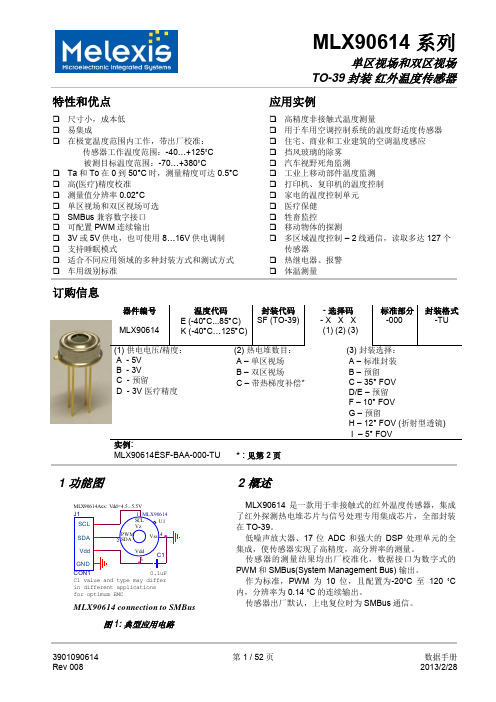
应用实例
高精度非接触式温度测量 用于车用空调控制系统的温度舒适度传感器 住宅、商业和工业建筑的空调温度感应 挡风玻璃的除雾 汽车视野死角监测 工业上移动部件温度监测 打印机、复印机的温度控制 家电的温度控制单元 医疗保健 牲畜监控 移动物体的探测 多区域温度控制 – 2 线通信,读取多达 127 个
PWM 引脚也可配置为热继电器(输入是 To),这样可以实现简单且性价比高的恒温控制器或温度报警(冰 点/沸点)应用,其中的温度临界值是用户可编程的。在 SMBus 系统里,这个功能可以作为处理器的中断信号, 以此触发读取主线上从动器的值,并确定精度条件。
传感器有两种供电电压选择:5V 或 3V(电池供电)。其中,5V 也可简便的从更高供电电压(例如 8 至 16V)上通过外接元件调制。(具体请参考“应用信息”)
第 1 / 52 页
数据手册 2013/2/28
LX90614 系列
单区视场和双区视场 TO-39 封装 红外温度传感器
概述(续)
MLX90614 集成了由 Melexis 研发生产的两款芯片: 红外热电堆探测器 MLX81101 专用信号处理芯片 MLX90302,专用于处理红外传感器的输出信号
传感器的测量结果均出厂校准化,数据接口为数字式的 PWM 和 SMBus(System Management Bus) 输出。
作为标准,PWM 为 10 位,且配置为-20˚C 至 120 ˚C 内,分辨率为 0.14 ˚C 的连续输出。
pt2201电源管理芯片引脚参数

pt2201电源管理芯片引脚参数
PT2201是一款电源管理芯片,用于管理锂离子电池的充电和放电过程。
以下是PT2201的主要引脚参数:
1. VCC:电源输入引脚,用于提供芯片所需的电源。
2. GND:接地引脚,用于将芯片连接到地线。
3. SNS:采样引脚,用于检测电池的电压和电流。
4. EN:使能引脚,用于控制芯片的开关。
5. FG:反馈引脚,用于接收外部电路的反馈信号。
6. CS:电流检测引脚,用于检测电池的充电电流。
7. CD:充电截止引脚,用于控制电池的充电截止电压。
8. DOUT:数据输出引脚,用于输出芯片的状态信息。
9. DIN:数据输入引脚,用于接收外部电路的控制信号。
需要注意的是,具体的引脚参数可能会因不同的应用场景而有所不同,因此在实际使用中需要参考相关的技术手册或数据表来了解详细的引脚参数和功能。
MEMORY存储芯片MAX202CWE+T中文规格书

●Saves Board Space •Integrated Charge Pump CircuitryEliminates the Need for a Bipolar ±12V SupplyEnables Single Supply Operation From Either +5Vor 9V to +12V•Integrated 0.1μF Capacitors (MAX203, MAX205)•24 pin SSOP Package Saves Up to 40% VersusSO Package●Saves Power for Longer Battery Operation•5μW Shutdown Mode (MAX200, MAX205,MAX206, MAX211)•75μW Ring Indicator Monitoring with Two ActiveReceivers (MAX213)Applications ●Battery-Powered Equipment ●Handheld Equipment ●Portable Diagnostics Equipment Selector Guide continued at end of data sheet.19-0065; Rev 8; 1/15PART POWER-SUPPLYVOLTAGE (V)NUMBER OF RS-232 DRIVERS NUMBER OF RS-232 RECEIVERS NUMBER OF RECEIVERS ACTIVE IN SHUTDOWN NUMBER OF EXTERNAL CAPACITORS (0.1μF)LOW-POWER SHUTDOWN/TTL THREE-STATE MAX200+55004Yes/No MAX201+5 and +9.0 to +13.22202No/No MAX202+52204No/No MAX203+5220None No/No General DescriptionMAX200-MAX209, MAX211, and MAX213 are a family of RS-232 and V.28 transceivers with integrated charge pump circuitry for single +5V supply operation.The drivers maintain the ±5V EIA/TIA-232E output signal levels at data rates in excess of 120kbps when loaded in accordance with the EIA/TIA-232E specification.The MAX211 and MAX213 are available in a 28-pin, wide small-outline (SO) package and a 28-pin shrink small-outline (SSOP) package, which occupies only 40% of the area of the SO. The MAX207 is available in a 24-pin SO package and a 24-pin SSOP . The MAX203 and MAX205 use no external components and are recommended for applications with limited circuit board space.Bene its and FeaturesSelector GuideTypical Operating Circuit 找MEMORY、二三极管上美光存储MAX200–MAX209/ MAX211/MAX213+5V, RS-232 Transceivers with 0.1μF External CapacitorsIntegrated │9MAX200 Pin Configuration/Typical Operating Circuit。
TLK2201EVM;中文规格书,Datasheet资料

IMPORTANT NOTICETexas Instruments and its subsidiaries (TI) reserve the right to make changes to their products or to discontinueany product or service without notice, and advise customers to obtain the latest version of relevant informationto verify, before placing orders, that information being relied on is current and complete. All products are soldsubject to the terms and conditions of sale supplied at the time of order acknowledgment, including thosepertaining to warranty, patent infringement, and limitation of liability.TI warrants performance of its semiconductor products to the specifications applicable at the time of sale inaccordance with TI’s standard warranty. Testing and other quality control techniques are utilized to the extentTI deems necessary to support this warranty. Specific testing of all parameters of each device is not necessarilyperformed, except those mandated by government requirements.Customers are responsible for their applications using TI components.In order to minimize risks associated with the customer’s applications, adequate design and operatingsafeguards must be provided by the customer to minimize inherent or procedural hazards.TI assumes no liability for applications assistance or customer product design. TI does not warrant or representthat any license, either express or implied, is granted under any patent right, copyright, mask work right, or otherintellectual property right of TI covering or relating to any combination, machine, or process in which suchsemiconductor products or services might be or are used. TI’s publication of information regarding any thirdparty’s products or services does not constitute TI’s approval, warranty or endorsement thereof.Copyright © 2000, Texas Instruments Incorporated/分销商库存信息: TITLK2201EVM。
ZWK060J12201JLX000中文资料(VISHAY)中文数据手册「EasyDatasheet - 矽搜」

16 20 POWER IN W
0
0
5
10
15
20
25
POWER IN W
温升
300
在K 温度
温升
300
ZWK 40
在K 温度
ZWK 60
200
200
100
100
0
0
10
20
30
40
50
0
0
20
40
60
80
100
温升
300
在K 温度
POWER IN W
温升
300
POWER IN W
ZWK 90
在K 温度
毫米[英寸]
ZWK 20 ZWK 20镍 15 ± 0.8 [0.602 ± 0.031] 81 ± 2 [3.189 ± 0.079] 14 [0.551] 13 [0.512] 5.5 [0.217]
D L DK LK d
模型
ZWK 40 ZWK 40镍 22 ± 1 [0.866 ± 0.039] 101 ± 2.5 [3.976 ± 0.098] 21 [0.827] 16 [0.63] 10 [0.394]
5.1 11
到36千欧 到360千欧
9.1
到62千欧
**请参阅文件"Vishay材料种类政策":
芯片中文手册,看全文,戳
水泥电阻器与套圈
全球产品编号信息
部分编号: ZWK010J11000KLX000
Z
模型
W
K
0
1
0
J
TCR /材料
1
1
0
值
0
0
EG-2001CA 106.2500M-PCHL0;EG-2001CA 125.0000M-PCHL0;中文规格书,Datasheet资料

OE pin = HIGH : Specified frequency output. OE pin = LOW : Output is high impedance
http://www.epsontoyocom.co.jp
/
分销商库存信息:
EPSON EG-2001CA 106.2500MPCHL0 EG-2021CA 125.0000MCGPNB EG-2001CA 125.0000MPCH0 EG-2001CA 125.0000MPCHL0 EG-2021CA 125.0000MCGPNL0 EG-2021CA 125.0000MCGPNL3 EG-2001CA 133.0000MPCHL3 EG-2001CA 106.2500MPCH0
EG-2001CA P: 50 5 % PCH PCY PCZ
External dimensions
EG-2021CA
#4 #3
5.0±0.2
(Unit:mm)
EG-2001CA
Footprint (Recommended) (Unit:mm)
#3
1.4
1.1
#4
1.4 #3
#4
1.1
1.8
1.5 3.9
fo
VCC T_stg T_use f_tol ICC I_dis SYM VOH VOL L_CMOS VIH VIL tr / tf t_str
OE=Vcc, No load condition OE=GND 50 % VCC level, L_CMOS Max. IOH = -8 mA IOL = 8 mA OE terminal Between 20% VCC and80% VCC level, L_CMOS Max. Time at minimum supply voltage to be 0 s Deterministic Jitter Random Jitter (RMS of total distribution) Peak to Peak Accumulated Jitter() n=2 to 50000 cycles Offset frequency: 12 kHz to 20 MHz
F2201资料

RF CHARACTERISTICS ( WATTS OUTPUT )2General DescriptionSilicon VDMOS and LDMOS transistors designed specifically for broadband RF applications. Suitable for Military Radios,Cellular and Paging Amplifier Base Stations, Broadcast FM/AM, MRI, Laser Driver and others.PATENTED GOLD METALIZED 2Watts Single Ended Package Style AP HIGH EFFICIENCY, LINEAR,ABSOLUTE MAXIMUM RATINGS (TC = 25 C)oTotal Device Junction to Case Thermal Maximum Junction StorageTemperatureDC Drain CurrentDrain to Gate Drain to Source Gate to Source 20Watts10Co 200-65to 1500.8A30VVV5050ELECTRICAL CHARACTERISTICS (EACH SIDE)SYMBOL PARAMETERMIN TYPMAXUNITS TEST CONDITIONSSYMBOL PARAMETERMIN TYPMAXUNITSTEST CONDITIONS GpsηVSWRCommon Source Power Gai Drain EfficiencyLoad Mismatch TolerancdB %Relative10500.220:1Idq = Idq = Idq = 0.20.2A,A,A,12.5Vds =V,12.5Vds =V,12.5Vds =V, F =850MHz F =850MHz F =850MHzBvdss Idss Igss Vgs gM Rdson Idsat Ciss Crss CossDrain Breakdown Voltag Zero Bias Drain Curren Gate Leakage Curren Gate Bias for Drain Curren Forward Transconductanc Saturation Resistanc Saturation CurrenCommon Source Input Capacitanc Common Source Feedback Capacitanc Common Source Output Capacitanc400.21710.222.37.51.28Mho Ohm Amp pF V V pF pFmA uA 0.01Ids = A,Vgs = 0V 12.5Vds =V,Vgs = 0V Vds = 0 V,Vgs = 30V 0.02Ids =A,Vgs = VdsVds = 10V,Vgs = 5V Vgs = 20V,Ids =1.6Vgs = 20V,Vds = 10V12.5Vds =V, Vgs = 0V, F = 1 MHz A 12.5Vds =V, Vgs = 0V, F = 1 MHz 12.5Vds =V, Vgs = 0V, F = 1 MHzPOLYFET RF DEVICES1110 Avenida Acaso, Camarillo, CA 93012 TEL:(805) 484-4210 FAX:(805) 484-3393 EMAIL:Sales@ URL:REVISION SILICON GATE ENHANCEMENT MODE RF POWER HIGH GAIN, LOW NOISE"Polyfet" process features gold metal for greatly extended lifetime. Low output capacitance and high F enhance broadband performancet TMC o Co C/Wo F2201polyfet rf devicesDissipation Resistance Temperature Voltage Voltage Voltage 8/1/97VDMOS TRANSISTORPOUT VS PIN GRAPHF2201POLYFET RF DEVICES1110 Avenida Acaso, Camarillo, CA 93012 TEL:(805) 484-4210 FAX:(805) 484-3393 EMAIL:Sales@ URL:CAPACITANCE VS VOLTAGEIV CURVE ID AND GM VS VGSS11 AND S22 SMITH CHART PACKAGE DIMENSIONS IN INCHESREVISION 8/1/97。
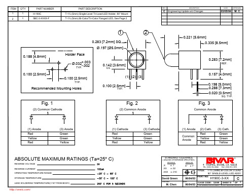
H190C-3;中文规格书,Datasheet资料
06/04/03
DATE:
TITLE: T-1¾ (5MM) BI-COLOR 3 LEAD 90° SINGLE-LEVEL LED ASSY REVISION: PART NO:
H190C-3-XX
C
M. Chen
06/04/03
CAGE CODE : 32559
SHEET # 1 OF
2
CAD GENERATED DOCUMENT, DO NOT MEASURE DRAWING.
REV.
DESCRIPTION
DATE
APPROVED
C
Engineering Update w/o Changes
03/05/04
M. C.
1
0.283 [7.2mm] SQ. Ø.197 [Ø5.0mm] 0.188 [4.8mm] Holder Face Ø.032+.003 -.002 TYP. 0.100 [2.5mm] 0.100 [2.5mm]
分销商库存信息:
BIVAR H190C-3
(1) Cathode Red Yellow Red
(3) Cathode Green Green Yellow
(1) Anode Common Anode
(2) Cath. Red Yellow Red
(3) Cath. Green Green Yellow
ABSOLUTE MAXIMUM RATINGS (Ta=25° C)
TYP.
2
0.221 [5.6mm] 0.335 [8.5mm]
0.283 [7.2mm] 0.142 [3.6mm]
C/L REF.
(1) (2) (3) 0.100 [2.5mm]