MPX12
飞思卡尔传感器

飞思卡尔传感器飞思卡尔传感器motorola/freescale氣壓傳感器MPX10D MPX10DP MPX10GP MPX10GS MPXV10GC6U MPXV10GC7U MPX12D MPX12DP MPX12GP MPX2010D MPX2010DP MPX2010GP MPXT2010G7U MPX2050D MPX2050DP MPX2050GP MPX2050GVP MPX2050GS MPX2050GSX MPX2050GVSX MPX2053D MPX2053DP MPX2053GP MPX2100A MPX2100DP MPX2100AP MPX2100AS MPX2100ASX MPX2102A MPX2102D MPX2102DP MPX2102AP MPX2102GP MPX2102GVP MPX2200A MPX2200D MPX2200DP MPX2200AP MPX2200GP MPX2200A MPX2200D MPX2200DP MP2200AP MPX2200GP MPX21002A MPX2102D MPX2102DP MPX2102AP MPX2102GP MPX2102GVP MPX2200A MPX2200D MPX2200DP MPX2200AP MPX2200GP MPX2201GP MPX2300DT1 MPX4080D MPX4100A MPXA4100A6U MPX4100AP MPXA4100A6U MPX4100AS MPX4101A MPXA4101AC6U MPX4105A MPX4115A MPXA4115A6U MPX4115AP MPXA4115AC6U MPX4115AS MPX4200A MPX4200AP MPX4200SA MPX4200ASX MPX4250A MPX4250AP MPX4250A6U MPXA4250A6T1 MPXA4250AC6U MPXA4250AC6T1 MPX4250D MPX4250GP MPX4250DP MPX5010D MPX5010DP MPX5010GP MPX5010GS MPX5010GSX MPXV5010G6U MPXV5010G7U MPXV5010GC6U/T1 MPXV5010GC7U MPX5050D MPX5050DP MPX5050GP MPX5100A MPX5100D MPX5100DP MPX5100AP MPX5100GP MPX5100GVP MPX5100AS MPX5100GS MPX5100GVS MPX5100ASX MPX5100GSX MPX5100GVSX MPX53D MPX53GP MPX5500D MPX5500DP MPX5700D MPX5700A MPX5700DP MPX5700GP MPX5700AP MPX5700GS MPX5700AS MPX5999D飞思卡尔传感器MPXA6115A6U MPXA6115AC6U MPXA6115A MPXA6115A6T1 MPXA6115AC6T1 MPXAZ4100A6U MPXAZ4100A MPXAZ4100A6T1 MPXAZ4100AC6U MPXAZ4100AC6T1 MPXAZ4115A6U MPXZ4115A MPXAZ4115A6T1 MPXAX4115AC6U MPXAZ4115AC6T1 MPXC2011DT1 MPXM2010D MPXM2010DT1 MPXM2010GS MPXM2010GST1 MPXM2053D MPXM2053DT1 MPXM2053GS MPXM2053GST1 MPXV4006GC6U MPXV4006G6U MPXV4115V6U MPXV4115V6T1 MPXV4115VC6U MPXV5004GC6U/T1 MPXV5004G6U/T1 MPXV5004GC7U MPXV5004G7U MPXY8010 MPXY8020 MPXY8030 MPXY8040 MMA6200xxQ 低重力加速度(low-g)傳感器MPXA6115A 高溫精確集成壓力傳感器MPXAZ6115A 耐抗高溫壓力傳感器MPXH6115A 高溫精確集成壓力傳感器MP3H6115A 高溫精確集成壓力傳感器 MPXHZ6115A 媒體耐抗的高溫精確集成壓力傳感器MPXH6250A 集成壓力傳感器 MPXH6300A 壓力傳感器 MPXH6400A 集成壓力傳感器等汽車用壓力傳感器飞思卡尔传感器图片飞思卡尔传感器技术参数:参数符号最小典型最大单位压力范围Pop 10 100 100 Kpa供电电压Vs 10 16 Vdc供电电流Io 6.0 mAdc满程输出Vfss 38.5 40 41.5 mV零位偏差电压Voff -1.0 0 1.0 mV灵敏度ΔV/ΔP 0.4 mV/Kpa线性度-0.25 0.25 %Vfs压力迟滞±0.25 %Vfs温度迟滞(-40~125℃)±0.5% %Vfs满程温度系数TCVFss -1.0 1.0 %Vfs零位温度系数TCVoff -1.0 1.0 mV输入阻抗Zin 1000 2500 Ω输出阻抗Zout 1400 3000 Ω响应时间TR 1.0 Ms稳定度±0.5 %Vfss最大压力 4 FS破坏压力7 FS工作温度TA -40~125 ℃以上内容技术参数以《OIML60号国际建议》92年版为基础,最新具体变化可查看《JJG669—12 Freescale广州南创传感器事业部检定规程》。
04.1 [BE]-MPX
![04.1 [BE]-MPX](https://img.taocdn.com/s3/m/f301ea2127d3240c8447efbc.png)
悬 挂 控 制
距
总 成
离 警 告
AFS ECU)
(大灯摆动
ECU 总成)
坐 椅 安 全 带 控 制
大 灯 水 平 测 量 电
大 灯 摆 动 电 机
机
ECU*11 ECU
*12
ECU*4
LH LH
5
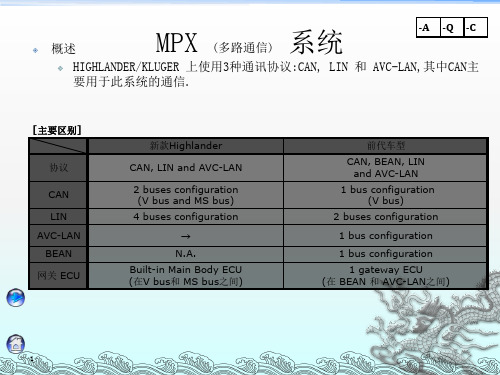
车型概述
发动机
底盘
MPX-MOST
MOST通信 --特性参数
车身
车身电器
协议 应用
MOST 音频视频
AVC-LAN + AVC-LAN
底盘
车身
元件位置
电源管理控制ECU
右侧接线盒
车身电器
转向锁执行器总成 转向锁ECU 主ECU(多路通信网络车身ECU) 左侧接线盒
22
车型概述
发动机
MPX系统-CAN
元件位置
底盘
车身
车身电器
大灯摆动控制ECU
大灯水平控制ECU
23
车型概述
发动机
MPX系统-CAN
元件位置
右侧车门通讯ECU
底盘
电动窗马 达
CANH, CANL
主/从 (单主) 星型
LIN
车型概述
发动机
底盘
MPX-MOST
MOST 通信 • 数据通信线和唤醒线
车身
车身电器
ACC
主设备(ECU) 显示器及导航模块显示屏
唤醒信号
从设备(ECU) 信号接收
MI+ MI-
信息唤醒电路 信息传达电路
WUO MO+ MO-
WUI MI+ MI-
信息唤醒电路 信息传达电路
ECU (副)
MPX

物理地址
这个号码是用作识别每一种部件(例如. 多媒体显 示, Navigation ECU,等)也能确定主要的部件
Logical Address
多媒体显示 这个号码是用作每一种功能(例如:功能按 钮,command 开关,调谐器等)Slave部件将这个号码 发送给主要的部件
Audio Head Unit 物理地址 190 (Audio Head Unit) 25 (Command 开关)
Gateway ECU
Mirror ECUs (D and P)
Power Source Control ECU Rain 感应器
Tilt and Telescopic ECU Double Lock ECU
EPS ECU J/C No. 2 Skid Control ECU*
2
Certification ECU
逻辑地址
29 (Speaker Beep)
60 (Radio Tuner), etc.
25
MPX 系统 of Recent Years
多总线传输 –近几年来,因为通讯系统数据量的增加和扩大,由CAN/BEAN等组 成的MPX系统被采用
AFS
ECU
TPWS
ECU
Meter
ECU
Sliding
Roof ECU
可变的结构 (min. 0 byte to max. 8 byte) Cyclic Redundancy 检查:提供一个错误检测的代码 与CRC的的报告向匹配 结构结束
6
0 - 64 15 2 7
15
MPX基本原理
CAN – 错误检测 • 与BEAN一样, CAN通过CRC检查发送的数据 • 如果是 “not good”: 在检测到错误以后,一个错误的信息会 立即产生并发送到各ECU里去
TEF6621中文资料

(USN)检测可控制立体声解调分离度 。 场强(LEVEL)、多径(WAM)和噪声 (USN)检测可控制高切断(HCC)。 场强(LEVEL)、多径(WAM)和噪声 (USN)检测可控制软静音。
典型应用
车载收音系统。
描述
2.6 表9 中频计数结果对应表
IFCN 4
0 0 0 0 0
IFCN 3
0 0 0 0 0
IFCN 2
0 0 0 0 1
1
1
1
1
1
1
IFCN 1 IFCN 0
0
0
0
1
1
0
1
1
0
0
。。。。。。
1
0
1
1
计数频率差
Байду номын сангаас
FM
AM
0KHz~5KHz
0KHZ~0.5KHz
5KHz~10KHz 0.5KHZ~1KHz
--
60
--
dB
--
0.5
0.8
%
45
60
--
dB
--
150
--
KHz
ftune(step)
调谐频率步距
欧洲/美国/日本模式
--
50
--
KHz
fIFc(res)
中频计数分辨率
--
5
--
KHz
Vo
L、R输出幅度
3h: OUTA=0
80
120
175
mV
AM部分
fRF Vi(sens)
AM射频频率
1.8寸彩屏 mpx ( mvs )播放器 操作说明

1.8寸彩屏mpx(mvs)播放器操作说明使用要点:1.本版本最好不要在W98下使用。
2.Win 2000 与PC联机后,不能直接脱离USB线。
一定要使用弹出方式安全删除硬件。
3.如出现Dos Error 显示时,需要您在本机的菜单中进行格式化。
4.使用FM必须要插耳机,否则不能收音。
5.充电说明:充电时最好把电源开关关掉,此时屏会不亮,最大的保护了OLED的寿命!如果想要边充电边听音乐则必须打开电源开关!本机为多媒体播放器(视频多媒体/MP3/FM/电子相册/图片浏览/游戏)。
采用26万色 160X128 点阵TFT彩屏,颜色亮丽;菜单界面美观大方。
本机可以对MPEG1/2的2/3层的所有压缩率以及取样率信号进行实时解码。
通过内置的麦克风,还可以进行SP(WAV)/LP(ASF)语音录音。
除了支持当前流行的多种音频文件格式外支持最新定义的视频多媒体文件,与传统的MP3文件不同,视频多媒体文件是包含有MP3的音频流和视频流的一种新的多媒体文件格式,通过本mpx(mvs)播放器,用户感受音频和视频于一体的全新感觉,是性价比最高的多媒体播放器。
MVS用户软件可以把Windows Media文件(*.wmv、*.wma、*.asf)和Mpeg文件 (*.mpg、*.mpeg)和Quick Time文件(*.mov、*.qt)和AVI文件(*.avi)压缩成本产品支持的视频格式(*.MVS)。
本机具有图片浏览,只需把图片做成BMP格式,大小最好为128X128 即可,如果超过128X128则可以按、上下移动或按、进行左右移动;最大为2048X2048;用户可根据自己喜好制作开机画面和待机屏保;ID3电脑软件编辑器支持编辑歌曲的ID3及歌词。
关于MVS视频文件说明MVS多媒体文件是由音频流和运动图像构成的多媒体文件,音频流的格式选用了当今流行的 MP3 音频编码格式。
目前可以把 DVD、VCD、Windows Media、Mpeg、Quick Time 、AVI 文件压缩成MVS文件,本机播放电影时可达到20祯/秒所以每分钟的MVS文件大小是约8M。
汽车中的MPX多路通信系统
仪表 多信息显示 (变换和设定 [adjustment])
多信息显示可以通过 “DISP” 开关来变换和设定
-A -Q -C
标准显示
设定显示
时钟设定
:设 置
其他巡航信息
显示设定
显示设定
: 回到标 准显示
空调显示
返回
无操作 (10 秒或更长)
: 按 (1秒内.)
9
: 按住 (1秒或更长)
: 设定 : 选择项目 : 返回标准显示画面
DRL) • H-LP LL Relay (w/
DRL) • H-LP RH, LH Relay
[IFL2]
• PBD Fuse • ALT Fuse • EPS Fuse • ST Fuse 发动机室继电器盒
Mechanical Relay • EFI MAIN Relay • A/F Relay • S-HORN Relay • HORN Relay • C/OPN Relay • H-LP RL Relay (w/o
(6)
(17)
注册快速语音
—
(6)
注册组
—
(20)
1自5 动音量设定
: 可以 —: 不可以 ( ): 最大输入容量 *: Only for –A models
系统图
蓝牙免提 系统
Overhead Module • 麦克风
多功能显示或音响机头组件*
“音量” 开关
组合仪表
• 车速
“语音” 开 关
DRL) • H-LP LL Relay (w/o
维修要点 IFL 能投过观察窗免拆检查是否熔断 (电力分配)
熔断部分
正常
熔断
5提示: PD 和 IFL1/2 为不可分解零件. 如果PD总成发生故障,则必
PTX-LCD 系列激励器说明书

PTX-LCD系列激励器说明书目 录1 概述 (3)1.1 综述 (3)1.2 激励器外观图 (3)1.3 激励器内部布局 (3)1.4 激励器原理框图 (4)1.5 技术指标 (5)2 操作 (8)2.1 面板布局及各功能键功能说明 (8)2.2 操作方法 (14)3 内部模块调整 (28)3.1 电源模块 (28)3.2 音频母板 (29)3.3 音频输入 (30)3.4 编码板 (32)3.5 锁相/驱动板及VCO板 (33)3.6 功率放大模块 (34)3.7 面板卡板 (35)3.8 CPU板 (37)3.9 遥测板(选件) (38)3.10 数字音频接口(AUDINP-DIG,选件) (38)3.11 基于DSP的数/模音频接口(TRDSP) (41)4 日常维护 (42)5 故障分析与维修 (43)5.1 液晶屏“白屏”或“全黑” (43)5.2 无音频或音频幅度低 (43)5.3 过载 (43)5.4 本振失锁 (43)1 概述1.1 综述PTX-LCD系列激励器采用19英寸标准机箱封装,频率调节灵活方便。
其频率范围涵盖87.5~108MHz,可10kHz步进设置。
如用户需要,亦可定制为其他频段。
按其最大输出功率,PTX-LCD系列可分为三种机型,PTX30-LCD为30W机,PTX60-LCD为60W机,PTX100-LCD为100W机,额定负载50Ω。
输出功率在0至标称值间任意可调。
现设备配置的机型为PTX30-LCD为30W机。
PTX-LCD可预置为立体声型或单声道/MPX型,单声道/MPX型可用于单声道信号或经外部编码器处理后的立体声信号的广播。
激励器的用户接口由液晶显示屏和一个旋钮(脉冲编码器)组成,操作简单明了。
借助此接口,使用者可参看所有的工作参数,并轻松调节可设置项如输出功率和工作频率。
激励器提供各种连接口,可使其集成到复合系统中。
它易于与外部单元如放大器、转换系统及同轴继电器等交流信息并提供控制,亦可与其它调制器组成网络。
串口模块MP3模块使用说明书

MPx 系列高保真放音模块根据存储介质的不同可分为 TF 卡版本(简称 T 版)、SD 卡版本(简称 S 版)和 FLASH 版本(简称 F 版)。其中 T 版体积小巧,节省空间;S 版具有最高性能价格比;F 版 专为震动场合设计,功能可靠。另有低成本 SPI 版本正在开发中,敬请期待。
MPx 系列高保真放音模块的推荐使用电压为 6V-24V,最低可低至 5V,最高可高达 30V,满足大 多数场合的需要。
MPx 系列高保真放音模块直接使用标准的内存卡存储音乐,通过电脑录音编辑后即可直接通过 非常廉价的读写卡器写入内存卡中,不使用昂贵且通用性差的专业编程器,在满足灵活性的前提下 最大限度为用户节省成本。
MPx 系列高保真放音模块使用非常简便,配合本公司提供的免费技术支持和驱动程序,可最大 限度的缩短用户的开发时间。
MPx 系列高保真放音模块有非常灵活的工作模式可供选择使用:MP3 模式、循环直放模式、普通 直放模式、并行模式和串行模式。
MPx 系列高保真放音模块可是以最简便的方式使用在各种各样需要高保真音响的场合:商场等 需要背景音的公共场合、各种游乐设备音响系统、学校等各种定时播放音乐的场合……
二、MP38x 系列放音模块选型表及全部照片
型号 MP380 MP383 MP385 MP386 MP381
型号 MP380
MP383
MP385
MP386
MP381
主要特点 存储介质
基本型 可扩展型 SD 卡座横置 可加功放型
- 1、下载文档前请自行甄别文档内容的完整性,平台不提供额外的编辑、内容补充、找答案等附加服务。
- 2、"仅部分预览"的文档,不可在线预览部分如存在完整性等问题,可反馈申请退款(可完整预览的文档不适用该条件!)。
- 3、如文档侵犯您的权益,请联系客服反馈,我们会尽快为您处理(人工客服工作时间:9:00-18:30)。
MPX12Rev 11, 07/2009Freescale Semiconductor © Freescale Semiconductor, Inc., 2007-2009. All rights reserved.10 kPa Uncompensated Silicon Pressure SensorsThe MPX12 series silicon piezoresistive pressure sensors provide a very accurate and linear voltage output, directly proportional to the applied pressure. This standard, low cost, uncompensated sensor permits manufacturers to design and add their own external temperaturecompensating and signal conditioning networks. Compensation techniques are simplified because of the predictability of Freescale's single element strain gauge design.Features•Low Cost•Patented Silicon Shear Stress Strain Gauge Design •Ratiometric to Supply Voltage•Easy to Use Chip Carrier Package Options •Gauge Options•Durable Epoxy PackageORDERING INFORMATIONDevice NamePackage Options Case No.# of PortsPressure Type Device Marking None SingleDualGaugeDifferentialAbsoluteUnibody Package (MPX12 Series)MPX12D Tray 344••MPX12D MPX12DP Tray 344C ••MPX12DP MPX12GP Tray 344B ••MPX12GPSmall Outline Package (MPXV12 Series)MPXV12DP Tray 1351••MPXV12DP MPXV12GP Tray 1369••MPXV12GP MPXV12GW6U Rail 1735••MPXV12GW MPXV12GW7U Rail 1560••MPXV12GW MPAK Package (MPXM12 Series)MPXM12GS Rail 1320A ••MPXM12GS MPXM12GST1Tape & Reel1320A••MPXM12GSMPX120 to 10 kPa (0 to 1.45 psi)55 mV Full Scale Span(Typical)SeriesApplication Examples•Air Movement Control•Environmental Control Systems •Level Indicators •Leak Detection•Medical Instrumentation •Industrial Controls•Pneumatic Control Systems •RoboticsMPX12SensorsSMALL OUTLINE PACKAGESMPX12GPCASE 344B-01MPX12D CASE 344-15MPX12DP CASE 344C-01UNIBODY PACKAGESMPXV12DP CASE 1351-01MPXV12GP CASE 1369-01MPXV12GW7U CASE 1560-02MPXV12GW6U CASE 1735-02MPAK PACKAGEMPXM12GS/GST1CASE 1320A-02MPX12SensorsOperating CharacteristicsTable 1. Operating Characteristics (V S = 3.0 Vdc, T A = 25°C unless otherwise noted, P1 > P2)CharacteristicSymbol Min Typ Max Unit Differential Pressure Range (1)1. 1.0 kPa (kiloPascal) equals 0.145 psi.P OP 0—10kPa Supply Voltage (2)2.Device is ratiometric within this specified excitation range. Operating the device above the specified excitation range may induce additional error due to device self-heating. V S — 3.0 6.0Vdc Supply Current I o — 6.0—mAdc Full Scale Span (3)3.Full Scale Span (V FSS ) is defined as the algebraic difference between the output voltage at full rated pressure and the output voltage at the minimum related pressure.V FSS 455570mV Offset (4)4.Offset (V OFF ) is defined as the output voltage at the minimum rated pressure.V off 02035mV Sensitivity ΔV/ΔP — 5.5—mV/kPa Linearity—–0.5— 5.0%V FSS Pressure Hysteresis (6) (0 to 10 kPa)——±0.1—%V FSS Temperature Hysteresis (–40°C to +125°C)——±0.5—%V FSS Temperature Coefficient of Full Scale Span TCV FSS –0.22—–0.16%V FSS /°C Temperature Coefficient of Offset TCV off —±15—μV/°C Temperature Coefficient of Resistance TCR 0.21—0.27%Z in /°C Input Impedance Z in 400—550ΩOutput ImpedanceZ out 750—1250ΩResponse Time (5) (10% to 90%)5.Response Time is defined as the time form the incremental change in the output to go from 10% to 90% of its final value when subjected to a specified step change in pressure. t R — 1.0—ms Warm-Up Time (6)6.Warm-up Time is defined as the time required for the product to meet the specified output voltage after the pressure is stabilized.——20—ms Offset Stability (7)7.Offset stability is the product’s output deviation when subjected to 1000 hours of Pulsed Pressure, Temperature Cycling with Bias Test.——±0.5—%V FSSMPX12SensorsMaximum RatingsFigure 1 shows a block diagram of the internal circuitry integrated on a pressure sensor chip.Figure 1. Uncompensated Pressure Sensor SchematicVoltage Output versus Applied Differential PressureThe output voltage of the differential or gauge sensor increases with increasing pressure applied to the pressure side (P1) relative to the vacuum side (P2). Similarly, outputvoltage increases as increasing vacuum is applied to the vacuum side (P2) relative to the pressure side (P1).Table 2. Maximum Ratings (1)1.Exposure beyond the specified limits may cause permanent damage or degradation to the device.RatingSymbol Value Unit Maximum Pressure (P1 > P2)P MAX 75kPa Burst Pressure (P1 > P2)P BURST 100kPa Storage Temperature T STG –40 to +125°C Operating TemperatureT A–40 to +125°C1234GND+V OUT–V OUT+V SSensing ElementMPX12SensorsTemperature CompensationFigure 2 shows the typical output characteristics of the MPX12 series over temperature.Because this strain gauge is an integral part of the silicon diaphragm, there are no temperature effects due todifferences in the thermal expansion of the strain gauge and the diaphragm, as are often encountered in bonded strain gauge pressure sensors. However, the properties of the strain gauge itself are temperature dependent, requiring that the device be temperature compensated if it is to be used over an extensive temperature range.Temperature compensation and offset calibration can be achieved rather simply with additional resistive components, or by designing your system using the MPX2010D series sensor.Several approaches to external temperaturecompensation over both –40 to +125°C and 0 to +80°C ranges are presented in Applications Note AN840.LINEARITYLinearity refers to how well a transducer's output follows the equation: V OUT = V OFF + sensitivity x P over the operating pressure range (Figure 3). There are two basic methods for calculating nonlinearity: (1) end point straight line fit or (2) a least squares best line fit. While a least squares fit gives the “best case” linearity error (lower numerical value), the calculations required are burdensome.Conversely, an end point fit will give the “worst case” error (often more desirable in error budget calculations) and the calculations are more straightforward for the user.Freescale’s specified pressure sensor linearities are based on the end point straight line method measured at the midrange pressure.Figure 2. Output vs. Pressure DifferentialFigure 3. Linearity Specification ComparisonPressure DifferentialO u t p u t (m V d c )8070605040302010000.32.00.64.00.96.01.28.0101.5PSI kPaSpan Range (Typ)Offset (Typ)V S = 3 V DC P1 > P2-40°C+25°C+125°CO u t p u t (m V d c )70605040302010080MPX12SensorsFigure 4. Cross-Sectional Diagram (not to scale)Figure 4 illustrates the differential/gauge die. A gel isolates the die surface and wire bonds from the environment, while allowing the pressure signal to be transmitted to the silicon diaphragm.Operating characteristics, internal reliability andqualification tests are based on use of dry clean air as thepressure media. Media other than dry clean air may have adverse effects on sensor performance and long termreliability. Contact the factory for information regarding media compatibility in your application.PRESSURE (P1)/VACUUM (P2) SIDE IDENTIFICATION TABLEFreescale designates the two sides of the pressure sensor as the Pressure (P1) side and the Vacuum (P2) side. The Pressure (P1) side is the side containing gel which isolates the die from the environment. Freescale’s MPx12 series is designed to operate with positive differential pressure applied, P1 > P2.The Pressure (P1) side may be identified by using the following tableGel Die CoatWire BondDieP1Stainless Steel CapThermoplasticCaseDie BondDifferential SensingElementP2Lead FramePart Number Case TypePressure (P1) SideIdentifier MPX12D 344Stainless Steel Cap MPX12DP 344C Side with Part Marking MPX12GP 344B Side with Port Attached MPXV12DP 1351Side with Part MarkingMPXV12GP 1369Side with Port MPXV12GW6U 1735 Side with Port MPXV12GW7U 1560 Side with Port MPXM12GS/GST11320ASide with Port AttachedISSUE BUNIBODY PACKAGEMPX12 SensorsMPX12SensorsCASE 1351-01ISSUE ASMALL OUTLINE PACKAGEMPX12 SensorsISSUE ASMALL OUTLINE PACKAGEMPX12SensorsISSUE OSMALL OUTLINE PACKAGEMPX12 SensorsISSUE BSMALL OUTLINE PACKAGEMPX12SensorsISSUE BSMALL OUTLINE PACKAGEMPX12 SensorsISSUE BSMALL OUTLINE PACKAGEMPX12SensorsISSUE DSMALL OUTLINE PACKAGEMPX12 SensorsISSUE DSMALL OUTLINE PACKAGEMPX12SensorsISSUE DSMALL OUTLINE PACKAGEMPX12 SensorsISSUE AMPAK PACKAGEMPX12SensorsCASE 1320A-02ISSUE AMPAK PACKAGEMPX12 SensorsMPX12Rev. 11How to Reach Us:Home Page:Web Support:/support USA/Europe or Locations Not Listed:Freescale Semiconductor, Inc.Technical Information Center, EL5162100 East Elliot Road Tempe, Arizona 852841-800-521-6274 or +/supportEurope, Middle East, and Africa:Freescale Halbleiter Deutschland GmbH Technical Information Center Schatzbogen 781829 Muenchen, Germany +44 1296 380 456 (English)+46 8 52200080 (English)+49 89 92103 559 (German)+33 1 69 35 48 48 (French)/supportJapan:Freescale Semiconductor Japan Ltd.Headquarters ARCO Tower 15F1-8-1, Shimo-Meguro, Meguro-ku,Tokyo 153-0064Japan0120 191014 or +81 3 5437 9125support.japan@ Asia/Pacific:Freescale Semiconductor China Ltd.Exchange Building 23F No. 118 Jianguo Road Chaoyang District Beijing 100022 China+86 010 5879 8000@For Literature Requests Only:Freescale Semiconductor Literature Distribution Center 1-800-441-2447 or +1-303-675-2140Fax: +1-303-675-2150LDCForFreescaleSemiconductor@Information in this document is provided solely to enable system and software implementers to use Freescale Semiconductor products. There are no express or implied copyright licenses granted hereunder to design or fabricate any integrated circuits or integrated circuits based on the information in this document.Freescale Semiconductor reserves the right to make changes without further notice to any products herein. Freescale Semiconductor makes no warranty, representation or guarantee regarding the suitability of its products for any particular purpose, nor does Freescale Semiconductor assume any liability arising out of the application or use of any product or circuit, and specifically disclaims any and all liability, including without limitation consequential or incidental damages. “Typical” parameters that may beprovided in Freescale Semiconductor data sheets and/or specifications can and do vary in different applications and actual performance may vary over time. All operating parameters, including “Typicals”, must be validated for each customer application by customer’s technical experts. Freescale Semiconductor does not convey any license under its patent rights nor the rights of others. Freescale Semiconductor products are not designed, intended, or authorized for use as components in systems intended for surgical implant into the body, or other applications intended to support or sustain life, or for any other application in which the failure of the Freescale Semiconductor product could create a situation where personal injury or death may occur. Should Buyer purchase or use Freescale Semiconductor products for any such unintended orunauthorized application, Buyer shall indemnify and hold Freescale Semiconductor and its officers, employees, subsidiaries, affiliates, and distributors harmless against all claims, costs, damages, and expenses, and reasonable attorney fees arising out of, directly or indirectly, any claim of personal injury or death associated with such unintended or unauthorized use, even if such claim alleges that Freescale Semiconductor was negligent regarding the design or manufacture of the part. Freescale™ and the Freescale logo are trademarks of Freescale Semiconductor, Inc.All other product or service names are the property of their respective owners.© Freescale Semiconductor, Inc. 2009. All rights reserved.。