CY7C4281-25JC中文资料
KOYO ELECTRONICS INDUSTRIES CO., LTD. GC7系列可编程触摸面板

352Visit our websitehttp://www.koyoele.co.jp/english/KOYO ELECTRONICS INDUSTRIES CO., LTD.GENERAL CATALOG 2014Latest catalog (free) is available online.Visual ScopeGC7FeaturesProgrammable Touch Panel (GC Type)Inherited the GC-5 display.- 10.4-inch TFT color Model number: GC-76LC - 5.7-inch STN color Model number: GC-73LCL-R- 5.7-inch STN monochrome Model number: GC-73LM-RFeatures- Shifted from the GC50 series.The applications of the GC-50 series (GC-53LC3, GC-53LM3, and sGC-56LC2) are partially inherited.The applications can be replaced within restrictions.Restrictions from the GC50 Series1. Drawing softwarePrepare ScreenCreator5 Ver3.0 or later.You can download the drawing software from Koyo Electronics' websitefree of charge.2. Panel cutout dimensionsThe panel cutout dimensions are not changed.The display can be installed in the existing holes for attaching the controlpanel as is.3. DimensionsThe 5.7-inch type is 7.1 mm thicker in depth. The 0.4-inch type is 3.0 mm wider in width.Since the location and size of mounting brackets and external connectionconnectors are different, make sure that there are no interfering parts inside and outside the board.4. Power SupplyThe 5.7-inch type is connected to the main body, not by terminal blockbut by connector (bundled item). The 10.4-inch type has been changed to 24 V DC speci cation.If you use the GC7 at 100 V/200 V AC, use the optional EA-AC orprepare a commercial AC/DC power supply. (If the EA-AC is used, the depth of the product becomes the main body + 36.1 mm.)5. Con firmation of PLC modelsPLCs that can be used are largely limited. Also, the shapes of connectionconnectors are different. (M:N communications also cannot be used.)6. Con firmation of peripheral devicesThe GC70 series has only one serial port.Also note that there are no parallel ports or RAS output / reset input.- ScreenCreator5 is usable.The ScreenCreator5 drawing software has been upgraded. You can draw in the same way as with the GC-50 series.7. Touch panel operationSince an analog-type touch panel is used, there are the following restrictions.- You cannot press two, three, or four points at the same time. - The resolution of the touch panel is different.Since the GC50 series has a different resolution (16 x 12 or 32 x 24) from the GC70 series (1,024 x 1,024), the operational feeling may be different.8. When K-BASIC is usedThere are restrictions on usable instruction words.9. When option products are usedThe digital I/O cannot be used.The backup data in a CF card is not compatible. If the data is backed up by a CF card for the GC50 series, restore the screen data to ScreenCreator5 once. Each setting data needs to be reset for the GC70 series.10.How to download screen dataScreen data can be transferred via USB.11.OtherThere may be restrictions in addition to the items mentioned above.Viewing angle of the screen, appearance of reduced / enlarged characters, appearance of the black-and-white type (difference between blue type LCD and black-and-white mode), etc.* When you change models, it is recommended that you check the operations using actual equipment once.353KOYO ELECTRONICS INDUSTRIES CO., LTD.GENERAL CATALOG 2014The specifications and prices described in this catalog were valid when the catalog was issued.For the latest information, contact our sales persons or see our website.Visual Scope GC7SpecificationsHow to Transfer SoftwareRead the screen data project using ScreenCreator5 (Ver3.0 or later).Change the target panel to the new model (GC-73LM-R / GC-73LCL-R / GC-76LC) using ScreenCreator5 (Ver3.0 or later).Recompile the screen data using ScreenCreator5 (Ver3.0 or later).Download the compilation data to the new model using ScreenCreator5 (Ver3.0 or later).* In a new model, it is not necessary to change to the download mode at hardware side like previous models.If the computer and the display are connected via a USB cable and the data is downloaded from a computer, the display automatically changes to the download mode and automatically restarts after the completion of the download.Each Part Names and Descriptions1 Power supply (24 V DC) Can be used for the power supply in the same conditions as GC-53L 3.2 CF card slotThe screen data can be uploaded/downloaded from a CF card.3 AC power supply module (Option) Can be used with a power supply under the same conditions as the GC-56LC2.4 Various LEDs You can check the power supply / status / transmission and reception.5 Battery Retain clock data / SRAM.6 Serial port For connection to a PLC7 USB A port The screen data can be uploaded/downloaded from a USB memory. 8 USB B port The screen data can be uploaded/downloaded from drawing software.Cable length: 3 mNot in Use4 Various LEDs3 AC Power Supply Module (Option)7 USB A Port8 USB B Port5 Battery6 Serial Port2 CF Card Slot 1StandardExpansion (Option is installed)354Visit our websitehttp://www.koyoele.co.jp/english/KOYO ELECTRONICS INDUSTRIES CO., LTD.GENERAL CATALOG 2014Latest catalog (free) is available online.Visual Scope GC7Specifications*1 Since this display uses a cold-cathode tube for the backlight, the brightness widely uctuates according to the conditions shown below. Consider the described brightness as a target. Ambient temperature, installation angle of the product, elapsed time since power-on, duration of use of the product, and number of product power supply ON/OFF cycles *2 Only the speci c card can be used.* Regarding the EA-AC speci cations, see P.349.355KOYO ELECTRONICS INDUSTRIES CO., LTD.GENERAL CATALOG 2014The specifications and prices described in this catalog were valid when the catalog was issued.For the latest information, contact our sales persons or see our website.Visual Scope GC7SpecificationsSupported PLCs as of May 2012Largely restricted compared with the GC50 series.If devices other than those above are connected, it is impossible to shift to the GC70 series.356Visit our websitehttp://www.koyoele.co.jp/english/KOYO ELECTRONICS INDUSTRIES CO., LTD.GENERAL CATALOG 2014Latest catalog (free) is available online.Visual ScopeHole12.1inch15.0inch357KOYO ELECTRONICS INDUSTRIES CO., LTD.GENERAL CATALOG 2014The specifications and prices described in this catalog were valid when the catalog was issued.For the latest information, contact our sales persons or see our website.Visual Scope GC7Correlation。
普通及机械结构用钢板GB与JIS对照
普通及机械结构用钢板GB与JIS对照1、日本钢材(JIS系列)的牌号中普通结构钢主要由三部分组成第一部分表示材质,如:S(Steel)表示钢,F(Ferrum)表示铁;第二部分表示不同的形状、种类、用途,如P(Plate)表示板,T(Tube)表示管,K(Kogu)表示工具,U—特殊用途,W—线材、丝,C—铸件,F—锻件;第三部分采用数字,表示钢类或钢材的序号或强度值下限。
有的牌号在数字序号后还附加后缀A、B、C等字母,表示不同的质量等级、种类或厚度。
如:SS400——第一个S表示钢(Steel),第二个S表示“结构”(Structure),400为下限抗拉强度400MPa,整体表示抗拉强度为400 MPa的普通结构钢。
在牌号主体结构(第一、二、三部分)之后,根据需要,可附加钢材形状、制造方法及热处理的后缀符号。
2、主要牌号说明:SPHC——首位S为钢Steel的缩写,P为板Plate的缩写,H为热Heat的缩写,C商业Commercial的缩写,整体表示一般用热轧钢板及钢带。
SPHD——表示冲压用热轧钢板及钢带。
SPHE——表示深冲用热轧钢板及钢带。
SPCC——表示一般用冷轧碳素钢薄板及钢带,相当于中国Q195-215A牌号。
其中第三个字母C为冷Cold的缩写。
需保证抗拉试验时,在牌号末尾加T为SPCCT。
SPCD——表示冲压用冷轧碳素钢薄板及钢带,相当于中国08AL(13237)优质碳素结构钢。
SPCE——表示深冲用冷轧碳素钢薄板及钢带,相当于中国08AL(5213)深冲钢。
需保证非时效性时,在牌号末尾加N为SPCEN。
冷轧碳素钢薄板及钢带调质代号:退火状态为A,标准调质为S,1/8硬为8,1/4硬为4,1/2硬为2,硬为1。
表面加工代号:无光泽精轧为D,光亮精轧为B。
如SPCC-SD表示标准调质、无光泽精轧的一般用冷轧碳素薄板。
再如SPCCT-SB 表示标准调质、光亮加工,要求保证机械性能的冷轧碳素薄板。
UPC4574G2-E1中文资料
UPC4574G2-E1中⽂资料The information in this document is subject to change without notice. Before using this document, please confirm that this is the latest version.Not all products and/or types are available in every country. Please check with an NEC Electronics sales representative for availability and additional information.DATA SHEETDocument No. G15977EJ4V0DS00 (4th edition)Date Published March 2004 N CP(K) Printed in JapanThe mark shows major revised points.1987DESCRIPTIONThe µPC4574 is an ultra low noise, high slew rate quad operational amplifier specifically designed for audio, instrumentation, and communication circuits. The low noise and high frequency capabilities make it ideal for preamps and active filters for instrumentation and professional audio.FEATURESUltra low noise High slew rate Wide bandwidthInternal frequency compensationORDERING INFORMATIONPart NumberPackageµPC4574C µPC4574C(5) 14-pin plastic DIP (7.62 mm (300)) 14-pin plastic DIP (7.62 mm (300)) µPC4574G2 µPC4574G2(5) 14-pin plastic SOP (5.72 mm (225)) 14-pin plastic SOP (5.72 mm (225))EQUIVALENT CIRCUIT (1/4 Circuit)I I I NVVPIN CONFIGURATION (Top View)OUT 4I I4I N4V ?I N3I I3OUT 3OUT 1I I1I N1V +I N2I I2OUT 2PC4574C, 4574C(5), 4574G2, 4574G2(5)µData Sheet G15977EJ4V0DS2ABSOLUTE MAXIMUM RATINGS (T A = 25°C)Parameter SymbolRatings Unit Voltage between V +and V ? Note1V +V0.3 to +36VDifferential Input Voltage V ID ±30 V Input VoltageNote2V IV ??0.3 to V ++0.3 V Output VoltageNote3V OV ??0.3 to V + +0.3VC Package Note4570 mW Power Dissipation G2 PackageNote5P T 550 mW Output Short Circuit DurationNote610 sec Operating Ambient Temperature T A ?20 to +80 °C Storage TemperatureT stg55 to +125°CNotes 1. Reverse connection of supply voltage can cause destruction.2. The input voltage should be allowed to input without damage or destruction. Even during the transition periodof supply voltage, power on/off etc., this specification should be kept. The normal operation will establish when the both inputs are within the Common Mode Input Voltage Range of electrical characteristics.3. This specification is the voltage which should be allowed to supply to the output terminal from externalwithout damage or destructive. Even during the transition period of supply voltage, power on/off etc., this specification should be kept. The output voltage of normal operation will be the Output Voltage Swing of electrical characteristics.4. Thermal derating factor is –7.6 mW/°C when ambient temperature is higher than 50°C.5. Thermal derating factor is –5.5 mW/°C when ambient temperature is higher than 25°C.6. Pay careful attention to the total power dissipation not to exceed the absolute maximum ratings, Note 4 andNote 5.RECOMMENDED OPERATING CONDITIONSParameter Symbol MIN. TYP. MAX. UnitSupply Voltage V ± ±4 ±16 V Output Current I O±10 mASource Resistance R S 50k ?Capacitive Load (A V = +1)C L 100 pFµPC4574C, µPC4574G2±Notes 7. Input bias currents flow out from IC. Because each currents are base current of PNP-transistor on input stage.8.This current flows irrespective of the existence of use.Data Sheet G15977EJ4V0DS 3µPC4574C(5), µPC4574G2(5)±Notes 7. Input bias currents flow out from IC. Because each currents are base current of PNP-transistor on input stage.8.This current flows irrespective of the existence of use.4Data Sheet G15977EJ4V0DSMEASUREMENT CIRCUITFig.1 Total Harmonic Distortion Measurement CircuitnFig.3 Flat Noise Measurement Circuit (FLAT+JIS A)V O = 40 dB x V n100 V n =V O40 dBData Sheet G15977EJ4V0DS 5Data Sheet G15977EJ4V0DS6TYPICAL PERFORMANCE CHARACTERISTICS (T A = 25°C, TYP.) T A - Operating Ambient Temperature - ?CPOWER DISSIPATIONP T - T o t a l P o w e r D i s s i p a t i o n - m W800600400200020*********20406080100120110010 k 1 M 1 k 10100 k 10 Mf - Frequency - HzOPEN LOOP FREQUENCY RESPONSEA V - O p e n L o o p V o l t a g e G a i n - d BV ± = ±15 V202040608021.510.50?0.5?1?1.5?2T A - Operating Ambient Temperature - ?CINPUT OFFSET VOLTAGEV I O - I n p u t O f f s e t V o l t a g e - m V= ±15 VV ±each 5 samples data806040200?20550530510490470450T A - Operating Ambient Temperature - ?CINPUT BIAS CURRENTI B - I n p u t B i a s C u r r e n t - n A= ±15 VV ±f - Frequency - HzLARGE SIGNAL FREQUENCY RESPONSE V o m - O u t p u t V o l t a g e S w i n g - V p -p 01020301001 k 10 k 100 k 1 M 10 MV = ±15 V±R L = 10 k ?I O - Output Current - mAOUTPUT CURRENT LIMITV O - O u t p u t V o l t a g e - V±±5±10±15T A - Operating Ambient Temperature - ?CSUPPLY CURRENTI C C - S u p p l y C u r r e n t - m A12963204020060800V = ±15 V±SUPPLY CURRENTI C C - S u p p l y C u r r e n t - m A12963±10±20V - Supply Voltage - V±Data Sheet G15977EJ4V0DS7COMMON MODE INPUT VOLTAGE RANGE V I C M - C o m m o n M o d e I n p u t V o l t a g e R a n g e - V 20100±10±20V - Supply Voltage - V±VOLTAGE FOLLOWER PULSE RESPONSE V O - O u t p u t V o l t a g e - V10551002468t - Time - sµV = ±15 V ±A V = 1R L = 2 k ?INPUT NOISE VOLTAGE (FLAT + JIS A)V n - I n p u t N o i s e V o l t a g e - V r .m .s .1001010.1101001 k10 k100 kR S - Source Resistance - ?V = ±15 V±µf - Frequency - HzINPUT EQUIVALENT NOISE VOLTAGE DENSITY e n - I n p u t E q u i v a l e n t N o i s e V o l t a g e D e n s i t y - n V / H z20468100 1 k10 k 100 k10±R S = 100 VTOTAL HARMONIC DISTORTIONT H D - T o t a l H a r m o n i c D i s t o r t i o n - %10.0010.010.10.000110100 1 k10 k 100 kf - Frequency - HzV = ±15 V ±V O = 3 V r.m.s.A V = 1R L = 2 k ?Data Sheet G15977EJ4V0DS8PACKAGE DRAWINGS (Unit: mm)14-PIN PLASTIC DIP (7.62 mm (300))ITEM MILLIMETERS A 19.22±0.22.14 MAX.F I J D 1.32±0.12G 3.6±0.3C B 2.54 (T.P.)0.50±0.10R 0~15°H 0.51 MIN.K 7.62 (T.P.)L 6.4±0.23.554.3±0.2N 0.25NOTES1. Each lead centerline is located within 0.25 mm ofits true position (T.P.) at maximum material condition.2. ltem "K" to center of leads when formed parallel.P14C-100-300B1-3M 0.25+0.10?0.05Data Sheet G15977EJ4V0DS9ITEM B C I 14-PIN PLASTIC SOP (5.72 mm (225))D E G H J PMILLIMETERS 1.27 (T.P.)1.42 MAX.A 10.2±0.264.4±0.10.1±0.10.426.5±0.21.49+0.08?0.071.1±0.163°+7°?3°NOTEEach lead centerline is located within 0.1 mm ofits true position (T.P.) at maximum material condition.F 1.59+0.21?0.2K L M N 0.6±0.20.170.10.10+0.08?0.07S14GM-50-225B, C-6RECOMMENDED SOLDERING CONDITIONSThe µPC4574 should be soldered and mounted under the following recommended conditions.For soldering methods and conditions other than those recommended below, contact an NEC Electronics sales representative.For technical information, see the following website.Semiconductor Device Mount Manual (/doc/015a7dda76a20029bd642de6.html/pkg/en/mount/index.html)Type of Surface Mount DeviceµPC4574G2, 4574G2(5): 14-pin plastic SOP (5.72 mm (225))Process ConditionsSymbol Infrared Ray Reflow Peak temperature: 230°C or below (Package surface temperature),Reflow time: 30 seconds or less (at 210°C or higher),Maximum number of reflow processes: 1 time.IR30-00-1Vapor Phase Soldering Peak temperature: 215°C or below (Package surface temperature),Reflow time: 40 seconds or less (at 200°C or higher),Maximum number of reflow processes: 1 time.VP15-00-1Wave Soldering Solder temperature: 260°C or below, Flow time: 10 seconds or less,Maximum number of flow processes: 1 time,Pre-heating temperature: 120°C or below (Package surface temperature).WS60-00-1Partial Heating Method Pin temperature: 300°C or below,Heat time: 3 seconds or less (Per each side of the device).–Caution Apply only one kind of soldering condition to a device, except for "partial heating method", or thedevice will be damaged by heat stress.Type of Through-hole DeviceµPC4574C, 4574C(5): 14-pin plastic DIP (7.62 mm (300))Process ConditionsWave Soldering (only to leads) Solder temperature: 260°C or below, Flow time: 10 seconds or less.Partial Heating Method Pin temperature: 300°C or below,Heat time: 3 seconds or less (per each lead).Caution For through-hole device, the wave soldering process must be applied only to leads, and make sure that the package body does not get jet soldered.Data Sheet G15977EJ4V0DS10The information in this document is current as of March, 2004. The information is subject to change without notice. For actual design-in, refer to the latest publications of NEC Electronics data sheets or data books, etc., for the most up-to-date specifications of N EC Electronics products. N ot all products and/or types are available in every country. Please check with an N EC Electronics sales representative for availability and additional information.No part of this document may be copied or reproduced in any form or by any means without the prior written consent of NEC Electronics. NEC Electronics assumes no responsibility for any errors that may appear in this document.NEC Electronics does not assume any liability for infringement of patents, copyrights or other intellectual property rights of third parties by or arising from the use of NEC Electronics products listed in this document or any other liability arising from the use of such products. No license, express, implied or otherwise, is granted under any patents, copyrights or other intellectual property rights of NEC Electronics or others.Descriptions of circuits, software and other related information in this document are provided for illustrative purposes in semiconductor product operation and application examples. The incorporation of these circuits, software and information in the design of a customer's equipment shall be done under the full responsibility of the customer. NEC Electronics assumes no responsibility for any losses incurred by customers or third parties arising from the use of these circuits, software and information.While NEC Electronics endeavors to enhance the quality, reliability and safety of NEC Electronics products, customers agree and acknowledge that the possibility of defects thereof cannot be eliminated entirely. To minimize risks of damage to property or injury (including death) to persons arising from defects in NEC Electronics products, customers must incorporate sufficient safety measures in their design, such as redundancy, fire-containment and anti-failure features.NEC Electronics products are classified into the following three quality grades: "Standard", "Special" and "Specific".The "Specific" quality grade applies only to NEC Electronics products developed based on a customer-designated "quality assurance program" for a specific application. The recommended applications of an NEC Electronics product depend on its quality grade, as indicated below. Customers must check the quality grade of each NEC Electronics product before using it in a particular application."Standard":Computers, office equipment, communications equipment, test and measurement equipment, audioand visual equipment, home electronic appliances, machine tools, personal electronic equipment and industrial robots. "Special":Transportation equipment (automobiles, trains, ships, etc.), traffic control systems, anti-disastersystems, anti-crime systems, safety equipment and medical equipment (not specifically designed for life support). "Specific":Aircraft, aerospace equipment, submersible repeaters, nuclear reactor control systems, lifesupport systems and medical equipment for life support, etc.The quality grade of NEC Electronics products is "Standard" unless otherwise expressly specified in NEC Electronics data sheets or data books, etc. If customers wish to use NEC Electronics products in applications not intended by NEC Electronics, they must contact an NEC Electronics sales representative in advance to determine NEC Electronics' willingness to support a given application.(Note)(1)"NEC Electronics" as used in this statement means NEC Electronics Corporation and also includes itsmajority-owned subsidiaries.(2)"NEC Electronics products" means any product developed or manufactured by or for NEC Electronics (asdefined above).M8E 02. 11-1。
圆二色谱仪chirscan参数

圆二色谱仪chirscan参数全文共四篇示例,供读者参考第一篇示例:圆二色谱仪(Circular Dichroism Spectrometer,简称CD)是一种用于研究物质的圆二色性质的仪器。
圆二色性是指物质在吸收圆偏振光时所表现出的不对称吸收现象,可以提供关于分子结构、构象和手性等信息。
Chirascan是一款由Applied Photophysics公司(APC)推出的CD仪器,具有高灵敏度、高分辨率和广泛的应用范围。
Chirascan是一款便携式的圆二色谱仪,它可以实现快速、准确地测量生物分子、生物大分子和其他有机小分子的圆二色谱谱图。
Chirascan具有以下主要参数:1.波长范围:Chirascan能够在175nm至900nm的波长范围内进行测量,覆盖了紫外到可见光区域,可以满足不同光学活性化合物的测量需求。
2.分辨率:Chirascan具有高分辨率的优点,使得用户可以在光学活性化合物的吸收光谱中清晰地观察到特征峰和特征谷,从而准确分析样品的立体结构和手性信息。
3.灵敏度:Chirascan在测量过程中具有高灵敏度,可以探测到微量的光学活性物质,即使在低浓度下也可以获得可靠的数据。
4.自动化功能:Chirascan具有智能化的数据采集和分析软件,可以实现自动测量、自动校准和自动计算参数等功能,为用户提供便捷、快速的操作体验。
5.温控功能:Chirascan具有温控功能,可以在不同温度下进行测量,研究物质的热力学性质和温度对其圆二色性质的影响。
6.多种测量模式:Chirascan支持多种测量模式,包括扫描模式、定点模式、动力学扫描模式等,可以满足不同用户的测量需求。
Chirascan是一款功能强大、性能稳定的圆二色谱仪,广泛应用于生物医药、生物化学、药物研发、食品安全等领域。
它不仅可以帮助科研人员深入理解生物大分子的结构和功能,还可以为药物设计和合成提供重要信息。
随着科技的不断发展,Chirascan将在更多领域展现其应用潜力,为科学研究和产业发展做出更大贡献。
CY7C68013A-128AXC中文资料
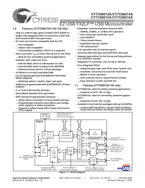
• CY7C68016A: Ideal for battery powered applications — Suspend current: 100 µA (typ) • CY7C68015A: Ideal for non-battery powered applications — Suspend current: 300 µA (typ) • Available in lead-free 56-pin QFN package (26 GPIOs) — 2 more GPIOs than CY7C68013A/14A enabling additional features in same footprint Cypress Semiconductor Corporation’s (Cypress’s) EZ-USB FX2LP (CY7C68013A/14A) is a low-power version of the EZ-USB FX2 (CY7C68013), which is a highly integrated, low-power USB 2.0 microcontroller. By integrating the USB 2.0 transceiver, serial interface engine (SIE), enhanced 8051 microcontroller, and a programmable peripheral interface in a single chip, Cypress has created a very cost-effective solution that provides superior time-to-market advantages with low power to enable bus powered applications. The ingenious architecture of FX2LP results in data transfer rates of over 53 Mbytes per second, the maximum-allowable USB 2.0 bandwidth, while still using a low-cost 8051 microcontroller in a package as small as a 56 QFN. Because it incorporates the USB 2.0 transceiver, the FX2LP is more economical, providing a smaller footprint solution than USB 2.0 SIE or external transceiver implementations. With EZ-USB FX2LP, the Cypress Smart SIE handles most of the USB 1.1 and 2.0 protocol in hardware, freeing the embedded microcontroller for application-specific functions and decreasing development time to ensure USB compatibility. The General Programmable Interface (GPIF) and Master/Slave Endpoint FIFO (8- or 16-bit data bus) provides
EN27C512中文资料(List Unclassifed)中文数据手册「EasyDatasheet - 矽搜」

4
芯片中文手册,看全文,戳
EN27C512
READ模式
该EN27C512具有两个控制功能,这两者必须逻辑满足以
获得在输出数据.芯片使能(
CE )是功率控制和应当用于
设备选择.输出使能(
OE )是输出控制和应使用栅极数据到
输出引脚,独立设备选择.假定地址是稳定,
地址访问时间(t
ACC )等于从延迟
在进入编程模式时12.75
± 0.25V被施加到
CE 是在V IL.用于编程,要编程数据被应用于与8位并行 数据引脚.
OE /VPP 销和
图5中QUIKRITE程TM序流程图显示EON交互式编程
算法.交互式算法采用20减少编程时间
编程脉冲和给每个地址仅尽可能多脉冲,是必要,以便
可靠地进行编程数据.之后每个脉冲被施加到一个给定地址,在该数据
30毫安操作(最大)
CMOS-和TTL兼容I / O
高可靠性CMOS技术
闭锁抗扰度100mA电流
从-1V到V CC + 1V二线控制(Βιβλιοθήκη OE & CE )
标准产品识别码
JEDEC标准引脚
28引脚PDIP
32引脚PLCC
28引脚TSOP(类型1)
商业和工业温度 范围
概述
所述EN27C512是一个低功率512Kbit,5V-只有一次性可编程(OTP)只读
芯片中文手册,看全文,戳
EN27C512 512KBIT EPROM (64K x 8)
EN27C512
特征
快速读取时间
:
-45,-55,-70,和-90ns
5V单电源供电
编程电压+ 12.75V
CY7C135-25JC中文资料

4K x 8 Dual-Port Static RAM and 4K x 8 Dual-PortSRAM with SemaphoresCY7C135CY7C1342Features•True Dual-Ported memory cells which allow simulta-neous reads of the same memory location •4K x 8 organization•0.65-micron CMOS for optimum speed/power •High-speed access: 15 ns•Low operating power: I CC = 160 mA (max.)•Fully asynchronous operation •Automatic power-down•Semaphores included on the 7C1342 to permit software handshaking between ports •Available in 52-pin PLCCFunctional DescriptionThe CY7C135 and CY7C1342 are high-speed CMOS 4K x 8 dual-port static RAMs. The CY7C1342 includes semaphores that provide a means to allocate portions of the dual-port RAM or any shared resource. Two ports are provided permitting in-dependent, asynchronous access for reads and writes to any location in memory. Application areas include interproces-sor/multiprocessor designs, communications status buffering, and dual-port video/graphics memory.Each port has independent control pins: chip enable (CE), read or write enable (R/W), and output enable (OE). The CY7C135 is suited for those systems that do not require on-chip arbitration or are intolerant of wait states. Therefore, the user must be aware that simultaneous access to a location is possible. Semaphores are offered on the CY7C1342 to as-sist in arbitrating between ports. The semaphore logic is com-prised of eight shared latches. Only one side can control the latch (semaphore) at any time. Control of a semaphore indi-cates that a shared resource is in use. An automatic pow-er-down feature is controlled independently on each port by a chip enable (CE) pin or SEM pin (CY7C1342 only).The CY7C135 and CY7C1342 are available in 52-pin PLCC.1342–1R/W L CE L OE LA 11L A 0LA 0RA 11R R/W R CE R OE RCE R OE R CE L OE L R/W LR/W RI/O 7L I/O 0LI/O 7R I/O 0RSEMAPHORE ARBITRATION (7C1342only)CONTROL I/O CONTROLI/O MEMORY ARRAYADDRESS DECODERADDRESS DECODER(7C1342only)SEMLSEMRLogic Block Diagram(7C1342only)Selection Guide7C135–157C1342–157C135–207C1342–207C135–257C1342–257C135–357C1342–357C135–557C1342–55Maximum Access Time (ns)1520253555Maximum Operating Current (mA)Commercial 220190180160160Maximum Standby Current for I SB1(mA)Commercial 6050403030Pin ConfigurationsA 11R 1V C C7C1342Top ViewPLCC 8910111213141516171819204645444342414039383736353421222324252627282930313233765432525150494847I /O I /O I /O I /O I /O I /O I /O I /O I /O I /O I /O 4L 5L 6L 7L0R 1R 2R 3R 4R 5R 6RN C G N D O E S E M A R /W C E R /W S E M 0LL L L L C E RR RA 10LA 10ROE R A 0R A 1R A 2R A 3R A 4R A 5R A 6R A 7R A 8R A 9R NC I/O 7RA 1LA 2L A 3L A 4L A 5L A 6L A 7L A 8L A 9L I/O 0L I/O 1L I/O 2L I/O 3L1V C C7C135Top ViewPLCC 8910111213141516171819204645444342414039383736353421222324252627282930313233765432525150494847I /O I /O I /O I /O I /O I /O I /O I /O I /O I /O I /O 4L 5L 6L 7L0R 1R 2R 3R 4R 5R 6RN C G N D O E N /C A R /W C E R /W 0LL L L C E R RA 10LA 10RR A 0R A 1R A 2R A 3R A 4R A 5R A 6R A 7R A 8R A 9R NC I/O 7RA 1LA 2L A 3L A 4L A 5L A 6L A 7L A 8L A 9L I/O 0L I/O 1L I/O 2L I/O 3LN /CA 11R A 11LA 11L1342–31342–4Pin DefinitionsLeft Port Right Port DescriptionA 0L–11L A 0R–11R Address Lines CE L CE R Chip Enable OE L OE R Output Enable R/W L R/W R Read/Write EnableSEM L(CY7C1342 only)SEM R(CY7C1342 only)Semaphore Enable. When asserted LOW, allows access to eight semaphores. The three least significant bits of the address lines will determine which semaphore to write or read. The I/O 0 pin is used when writing to a semaphore. Semaphores are requested by writing a 0 into the respective location.Maximum Ratings[1]Storage Temperature ..................................–65°C to +150°C Ambient Temperature withPower Applied..............................................–55°C to +125°C Supply Voltage to Ground Potential(Pin 48 to Pin 24)............................................–0.5V to +7.0V DC Voltage Applied to Outputsin High Z State................................................–0.5V to +7.0V DC Input Voltage[2].........................................–3.0V to +7.0V Static Discharge Voltage...........................................> 2001V (per MIL-STD-883, Method 3015)Latch-Up Current....................................................> 200 mA Operating RangeRangeAmbientTemperature V CC Commercial0°C to +70°C 5V ± 10%Industrial–40°C to +85°C5V ± 10%Electrical Characteristics Over the Operating Range[4]7C135–15 7C1342–157C135–207C1342–27C135–257C1342–25Parameter Description Test Conditions Min.Max.Min.Max.Min.Max.UnitV OH Output HIGH Voltage V CC = Min., I OH = –4.0 mA 2.4 2.4 2.4V V OL Output LOW Voltage V CC = Min., I OL = 4.0 mA0.40.40.4V V IH Input HIGH Voltage 2.2 2.2 2.2V V IL Input LOW Voltage0.80.80.8V I IX Input Load Current GND ≤ V I≤ V CC–10+10–10+10–10+10µA I OZ Output Leakage Current Outputs Disabled,GND ≤ V O≤ V CC–10+10–10+10–10+10µAI CC Operating Current V CC = Max.,I OUT = 0 mA Com’l220190180mA Ind.190I SB1Standby Current(Both Ports TTL Levels)CE L and CE R≥ V IH,f = f MAX[5]Com’l605040mAInd.50I SB2Standby Current(One Port TTL Level)CE L and CE R≥ V IH,f = f MAX[5]Com’l130120110mAInd.120I SB3Standby Current(Both Ports CMOS Levels)Both Ports CE and CE R≥V CC – 0.2V,V IN≥ V CC – 0.2Vor V IN≤ 0.2V, f = 0[5]Com’l151515mAInd.30I SB4Standby Current(One Port CMOS Level)One Port CE L orCE R≥ V CC – 0.2V,V IN≥V CC – 0.2V or V IN≤ 0.2V,Active Port Outputs, f =f MAX[5]Com’l125115100mAInd.115Notes:1.The Voltage on any input or I/O pin cannot exceed the power pin during power-up.2.Pulse width < 20 ns.3.T A is the “instant on” case temperature.4.See the last page of this specification for Group A subgroup testing information.5.f MAX = 1/t RC = All inputs cycling at f = 1/t RC (except output enable). f = 0 means no address or control lines change. This applies only to inputs at CMOS level standby I SB3.Electrical Characteristics Over the Operating Range [4](continued)7C135–357C1342–357C135–557C1342–55Parameter DescriptionTest ConditionsMin.Max.Min.Max.Unit V OH Output HIGH Voltage V CC = Min., I OH = –4.0 mA 2.42.4V V OL Output LOW VoltageV CC = Min., I OL = 4.0 mA0.40.4V V IH 2.22.2V V IL Input LOW Voltage 0.80.8V I IX Input Load Current GND ≤ V I ≤ V CC–10+10–10+10µA I OZ Output Leakage Current Outputs Disabled, GND ≤ V O ≤ V CC –10+10–10+10µA I CC Operating Current V CC = Max., I OUT = 0 mA Com’l 160160mAV CC = Max., I OUT = 0 mA Ind.180180I SB1Standby Current(Both Ports TTL Levels)CE L and CE R ≥ V IH , f = f MAX[5]Com’l 3030mA Ind.4040I SB2Standby Current (One Port TTL Level)CE L and CE R ≥ V IH , f = f MAX [5]Com’l 100100mA Ind.110110I SB3Standby Current (Both Ports CMOS Levels)Both Ports CE and CE R ≥ V CC – 0.2V , V IN ≥ V CC – 0.2Vor V IN ≤ 0.2V , f = 0[5]Com’l 1515mA Ind.3030I SB4Standby Current(One Port CMOS Level)One Port CE L or CE R ≥ V CC – 0.2V , V IN ≥ V CC – 0.2V or V IN ≤ 0.2V , Active Port Outputs, f = f MAX [5]Com’l 9090mA Ind.100100Capacitance [6]ParameterDescriptionTest ConditionsMax.Unit C IN Input Capacitance T A = 25°C, f = 1 MHz, V CC = 5.0V10pF C OUTOutput Capacitance10pFAC Test Loads and WaveformsNote:6.Tested initially and after any design or process changes that may affect these parameters.3.0V GND90%90%10%≤3ns≤3ns10%ALL INPUT PULSES(a) Normal Load (Load 1)R1=893Ω5VOUTPUTR1=347ΩC=30pFR TH =250ΩV TH =1.4VOUTPUTC=30pF(b) Thévenin Equivalent (Load 1)(c) Three-State Delay (Load 3)R TH =250ΩV XOUTPUTC =5pF1342–51342–61342–71342–8Switching Characteristics Over the Operating Range[7, 8]7C135–15 7C1342–157C135–207C1342–207C135–257C1342–257C135–357C1342–357C135–557C1342–55Parameter Description Min.Max.Min.Max.Min.Max.Min.Max.Min.Max.Unit READ CYCLEt RC Read Cycle Time1520253555ns t AA Address to Data Valid1520253555ns t OHA Output Hold FromAddress Change33333ns t ACE CE LOW to Data Valid1520253555ns t DOE OE LOW to Data Valid1013152025ns t LZOE[9,10,11]OE Low to Low Z33333ns t HZOE[9,10,11]OE HIGH to High Z1013152025ns t LZCE[9,10,11]CE LOW to Low Z33333ns t HZCE[9,10,11]CE HIGH to High Z1013152025ns t PU[11]CE LOW to Power Up00000ns t PD[11]CE HIGH to Power Down1520253555ns WRITE CYCLEt WC Write Cycle Time1520253555ns t SCE CE LOW to Write End1215203050ns t AW Address Set-Up to Write End1215203050ns t HA Address Hold from Write End22222ns t SA Address Set-Up to Write Start00000ns t PWE Write Pulse Width1215202550ns t SD Data Set-Up to Write End1013151525ns t HD Data Hold from Write End00000ns t HZWE[10,11]R/W LOW to High Z1013152025ns t LZWE[10,11]R/W HIGH to Low Z33333ns t WDD[12]Write Pulse to Data Delay3040506070ns t DDD[12]Write Data Valid to ReadData Valid2530303540ns SEMAPHORE TIMING[13]t SOP SEM Flag Update Pulse(OE or SEM)1010101515ns t SWRD SEM Flag Write to Read Time55555ns t SPS SEM Flag Contention Window55555ns Notes:7.See the last page of this specification for Group A subgroup testing information.8.Test conditions assume signal transition time of 3 ns or less, timing reference levels of 1.5V, input pulse levels of 0 to 3.0V, and output loading of the specifiedI OL/I OH and 30-pF load capacitance.9.At any given temperature and voltage condition for any given device, t HZCE is less than t LZCE and t HZOE is less than t LZOE.10.Test conditions used are Load 3.11.This parameter is guaranteed but not tested.12.For information on port-to-port delay through RAM cells from writing port to reading port, refer to Read Timing with Port-to-Port Delay waveform.13.Semaphore timing applies only to CY7C1342.Switching WaveformsNotes:14.R/W is HIGH for read cycle.15.Device is continuously selected, CE = V IL and OE = V IL .16.Address valid prior to or coincident with CE transition LOW.17.CE L = CE R =LOW; R/W L = HIGHt RCt AAt OHADATA VALIDPREVIOUS DATA VALIDDATA OUTADDRESSEither Port Address Access1342–9Read Cycle No. 1[14,15]t ACEt LZOEt DOEt HZOEt HZCEDATA VALIDDATA OUTSEMor CE OEt LZCEt PUI CC I SBt PDEither Port CE/OE Access1342–10Read Cycle No. 2[14,16][13]VALIDt DDDt WDDMATCHMATCHR/W RDATA INRDATA OUTLt wcADDRESS Rt PWEVALIDtSDtHDADDRESS L1342–11Read Timing with Port-to-Port [17]Notes:18.terminate a write by going HIGH. The data input set-up and hold timing should be referenced to the rising edge of the signal that terminates the write.19.R/W must be HIGH during all address transactions.20.If OE is LOW during a R/W controlled write cycle, the write pulse width must be the larger of t PWE or (t HZWE + t SD ) to allow the I/O drivers to turn off and data to be placed on thebus for the required t SD . If OE is HIGH during a R/W controlled write cycle (as in this example), this requirement does not apply and the write pulse can be as short as the specified t PWE .21.Switching Waveforms (continued)t AWt WCDATA VALIDHIGH IMPEDANCEt SCEt SAt PWEt HDt SDt HAt HZOEtLZOESEM OR CER/WADDRESS OEDATA OUTDATA IN1342–12Write Cycle No. 1: OE Three-States Data I/Os (Either Port)[18,19,20][13]t AWt WCt SCEt SAt PWEt HDt SDt HZWEt HAHIGH IMPEDANCESEM OR CER/WADDRESSDATA OUTDATA INt LZWEDATA VALID1342–13Write Cycle No. 2:R/W Three-States Data I/Os (Either Port)[19, 21][13]Notes:22.CE = HIGH for the duration of the above timing (both write and read cycle).23.I/O 0R = I/O 0L = LOW (request semaphore); CE R = CE L = HIGH.24.Semaphores are reset (available to both ports) at cycle start.25.If t SPS is violated, it is guaranteed that only one side will gain access to the semaphore.Switching Waveforms (continued)t SOPt AASEMR/WOEI/O 0VALID ADDRESSVALID ADDRESSt HDDATA IN VALIDDATA OUT VALIDt OHAA 0–A 2t AWt HAt ACEt SOPt SCEt SDt SAt PWEt SWRDt DOEWRITE CYCLEREAD CYCLE1342–14Semaphore Read After Write Timing, Either Side (CY7C1342 only)[22]MATCHt SPSA 0L –A 2LMATCHR/W L SEM LA 0R –A 2RR/W R SEM R1342–15Timing Diagram of Semaphore Contention (CY7C1342 only)[23,24,25]ArchitectureThe CY7C135 consists of an array of 4K words of 8 bits each of dual-port RAM cells, I/O and address lines, and control sig-nals (CE, OE, R/W). Two semaphore control pins exist for the CY7C1342 (SEM L/R).Functional DescriptionWrite OperationData must be set up for a duration of t SD before the rising edge of R/W in order to guarantee a valid write. Since there is no on-chip arbitration, the user must be sure that a specific loca-tion will not be accessed simultaneously by both ports or erro-neous data could result. A write operation is controlled by ei-ther the OE pin (see Write Cycle No. 1 timing diagram) or the R/W pin (see Write Cycle No. 2 timing diagram). Data can be written t HZOE after the OE is deasserted or t HZWE after the falling edge of R/W. Required inputs for write operations are summarized in Table 1.If a location is being written to by one port and the opposite port attempts to read the same location, a port-to-port flowthrough delay is met before the data is valid on the output. Data will be valid on the port wishing to read the location t DDD after the data is presented on the writing port.Read OperationWhen reading the device, the user must assert both the OE and CE pins. Data will be available t ACE after CE or t DOE after OE are asserted. If the user of the CY7C1342 wishes to ac-cess a semaphore, the SEM pin must be asserted instead of the CE pin. Required inputs for read operations are summa-rized in Table 1.Semaphore OperationThe CY7C1342 provides eight semaphore latches which are separate from the dual port memory locations. Semaphores are used to reserve resources which are shared between the two ports. The state of the semaphore indicates that a re-source is in use. For example, if the left port wants to request a given resource, it sets a latch by writing a zero to a sema-phore location. The left port then verifies its success in setting the latch by reading it. After writing to the semaphore, SEM or OE must be deasserted for t SOP before attempting to read the semaphore. The semaphore value will be available t SWRD + t DOE after the rising edge of the semaphore write. If the left port was successful (reads a zero), it assumes control over the shared resource, otherwise (reads a one) it assumes the right port has control and continues to poll the semaphore. When the right side has relinquished control of the semaphore (by writing a one), the left side will succeed in gaining control of the semaphore. If the left side no longer requires the sema-phore, a one is written to cancel its request.Semaphores are accessed by asserting SEM LOW. The SEM pin functions as a chip enable for the semaphore latches. CE must remain HIGH during SEM LOW. A0–2 represents the semaphore address. OE and R/W are used in the same man-ner as a normal memory access. When writing or reading a semaphore, the other address pins have no effect.When writing to the semaphore, only I/O0 is used. If a 0 is written to the left port of an unused semaphore, a one will appear at the same semaphore address on the right port. That semaphore can now only be modified by the side showing a zero (the left port in this case). If the left port now relinquishes control by writing a one to the semaphore, the semaphore will be set to one for both sides. However, if the right port had requested the semaphore (written a zero) while the left port had control, the right port would immediately own the sema-phore. Table 2 shows sample semaphore operations.When reading a semaphore, all eight data lines output the semaphore value. The read value is latched in an output reg-ister to prevent the semaphore from changing state during a write from the other port. If both ports request a semaphore control by writing a 0 to a semaphore within t SPS of each other, it is guaranteed that only one side will gain access to the sema-phore.Initialization of the semaphore is not automatic and must be reset during initialization program at power-up. All sema-phores on both sides should have a one written into them at initialization from both sides to assure that they will be free when needed.Table 1. Non-Contending Read/WriteInputs OutputsOperationCE R/W OE SEM I/O0 – I/O7H X X H High Z Power-DownH H L L Data Out ReadSemaphoreX X H X High Z I/O Lines DisabledH L X L Data In Write to Semaphore L H L H Data Out ReadL L X H Data In WriteL X X L Illegal Condition Table 2. Semaphore Operation ExampleFunctionI/O0-7LeftI/O0-7Right StatusNo Action11Semaphore freeLeft port writessemaphore01Left port obtainssemaphoreRight port writes 0 tosemaphore01Right side is deniedaccessLeft port writes 1 tosemaphore10Right port is grantedaccess to Sema-phoreLeft port writes 0 tosemaphore10No change. Left portis denied access Right port writes 1 tosemaphore01Left port obtainssemaphoreLeft port writes 1 tosemaphore11No port accessingsemaphore address Right port writes 0 tosemaphore10Right port obtainssemaphoreRight port writes 1 tosemaphore11No port accessingsemaphoreLeft port writes 0 tosemaphore01Left port obtainssemaphoreLeft port writes 1 tosemaphore11No port accessingsemaphoreTypical DC and AC Characteristics1008070600.01.02.03.05.05090V CC =5.0V T A =25°C 4.04.04.55.05.56.014012010080604001.02.03.0 5.0O U T P U T S O U R C E C U R R E N T (m A )SUPPLY VOLTAGE (V)NORMALIZED SUPPLY CURRENT vs. SUPPLY VOLTAGE NORMALIZED SUPPLY CURRENT vs. AMBIENT TEMPERATURE AMBIENT TEMPERATURE (°C)OUTPUT VOLTAGE (V)OUTPUT SOURCE CURRENT vs. OUTPUT VOLTAGE 0.0N O R M A L I Z E D I , I C C0I CC 1.21.11.00.9–55125N O R M A L I Z E D t A ANORMALIZED ACCESS TIME vs. AMBIENT TEMPERATURE AMBIENT TEMPERATURE (°C)1.051.004.04.55.0 5.56.0N O R M A L I Z E D t A ASUPPLY VOLTAGE (V)NORMALIZED ACCESS TIME vs. SUPPLY VOLTAGEO U T P U T S I N K C U R R E N T (m A )OUTPUT VOLTAGE (V)OUTPUT SINK CURRENT vs. OUTPUT VOLTAGE V CC =5.0VT A =25°C0.80.95 1.251.00.751050N O R M A L I Z E D I C C0.50NORMALIZED I CC vs.CYCLE TIME CYCLE FREQUENCY (MHz)1.00.750.2501.02.03.05.0N O R M A L I Z E D t P C20.010.05.00200400600800D E L T A t (n s )015.00.0SUPPLY VOLTAGE (V)TYPICAL POWER-ON CURRENT vs. SUPPLY VOLTAGE CAPACITANCE (pF)TYPICAL ACCESS TIME CHANGEvs. OUTPUT LOADING4.010000.50A A 2030I SBS BN O R M A L I Z E D I , I C CS B251.10V CC =4.5V T A =25°CV CC =5.0V T A =25°C V IN =0.5V401.00.60.41.20.220V CC =5.0V T A =25°C4.01.4–55251251.21.00.80.60.6V CC =5.0V V IN =5.0V I CC0.20.4I SB30.8Document #: 38-06038 Rev. *B Page 11 of 12© Cypress Semiconductor Corporation, 2004. The information contained herein is subject to change without notice. Cypress Semiconductor Corporation assumes no responsibility for the use of any circuitry other than circuitry embodied in a Cypress product. Nor does it convey or imply any license under patent or other rights. Cypress products are not warranted nor intended to be used for medical, life support, life saving, critical control or safety applications, unless pursuant to an express written agreement with Cypress. Furthermore, Cypress does not authorize its products for use as critical components in life-support systems where a malfunction or failure may reasonably be expected to result in significant injury to the user. The inclusion of Cypress products in life-support systems application implies that the manufacturer assumes all risk of such use and in doing so indemnifies Cypress against all charges.Ordering Information4K x8 Dual-Port SRAM Speed (ns)Ordering Code Package Name Package TypeOperating Range 15CY7C135–15JC J6952-Lead Plastic Leaded Chip Carrier Commercial 20CY7C135–20JC J6952-Lead Plastic Leaded Chip Carrier Commercial 25CY7C135–25JC J6952-Lead Plastic Leaded Chip Carrier Commercial CY7C135–25JI J6952-Lead Plastic Leaded Chip Carrier Industrial 35CY7C135–35JC J6952-Lead Plastic Leaded Chip Carrier Commercial CY7C135–35JI J6952-Lead Plastic Leaded Chip Carrier Industrial 55CY7C135–55JC J6952-Lead Plastic Leaded Chip Carrier Commercial CY7C135–55JIJ6952-Lead Plastic Leaded Chip CarrierIndustrial4K x8 Dual-Port SRAM with Semaphores Speed (ns)Ordering Code Package Type Package TypeOperating Range 15CY7C1342–15JC J6952-Lead Plastic Leaded Chip Carrier Commercial 20CY7C1342–20JC J6952-Lead Plastic Leaded Chip Carrier Commercial 25CY7C1342–25JC J6952-Lead Plastic Leaded Chip Carrier Commercial CY7C1342–25JI J6952-Lead Plastic Leaded Chip Carrier Industrial 35CY7C1342–35JC J6952-Lead Plastic Leaded Chip Carrier Commercial CY7C1342–35JI J6952-Lead Plastic Leaded Chip Carrier Industrial 55CY7C1342–55JC J6952-Lead Plastic Leaded Chip Carrier Commercial CY7C1342–55JIJ6952-Lead Plastic Leaded Chip CarrierIndustrialPackage Diagrams52-Lead Plastic Leaded Chip Carrier J6951-85004-*ADocument #: 38-06038 Rev. *B Page 12 of 12Document History PageDocument Title: CY7C135/CY7C1342 4K x 8 Dual Port Static RAM and 4K x 8 Dual Port Static RAM w/Semaphores Document Number: 38-06038REV.ECN NO.Issue Date Orig. of Change Description of Change**11018110/21/01SZV Change from Spec number: 38-00541 to 38-06038*A 12228812/27/02RBI Power up requirements added to Maximum Ratings Information *B236763SEE ECNYDTRemoved cross information from features section。
日本SHINKO神港温控器JC系列 中文选型说明书
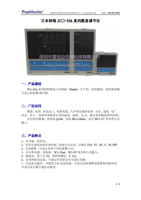
日本神港JC□-33A系列数显调节仪
一、产品描述
JC□-33A系列控制器是日本神港(Shinko)生产的一款高精度、低价格的数字显示控制器/调节器。
二、广泛应用
橡塑、纺织、食品加工、电线电缆、汽车和金属热处理、石化、造纸、电厂、冶金、轻工、科研等领域等行业的温度、湿度、压力、液位等参数的调节控制;
可以热电偶K、热电阻pt100、电流DC4-20mA、电压DC1-5V等多种方式输入。
三、产品特点
1、多功能,低价位;
2、采用先进的加热冷却控制;控制方式灵活;自整定PID、PI、PD、P、ON/OFF;
3、2组报警,可设定多种不同的报警方式;
4、可以热电偶、热电阻、DC4-20mA、DC1-5V等多种方式输入;
5、精度高,优于0.2%;采样周期短,0.25s;
6、自带两组设定值,可通过外部给定信号进行切换;
7、可追加功能多:可提供24V直流电源,可设定加热器断线报警和回路异常,可设定串行数字通信功能等。
四、日本shinko神港温控器JC系列简易选型表
注:更多相关产品、各行业温度控制系统解决方案详情、资料下载>>>>>>>>请进入普旭官网:
>>>>>>>>咨询热线:400-000-3990。
- 1、下载文档前请自行甄别文档内容的完整性,平台不提供额外的编辑、内容补充、找答案等附加服务。
- 2、"仅部分预览"的文档,不可在线预览部分如存在完整性等问题,可反馈申请退款(可完整预览的文档不适用该条件!)。
- 3、如文档侵犯您的权益,请联系客服反馈,我们会尽快为您处理(人工客服工作时间:9:00-18:30)。
64K/128K x 9 Deep Sync FIFOsCY7C4281CY7C4291Features•High-speed, low-power, first-in first-out (FIFO) memories•64K × 9 (CY7C4281)•128K × 9 (CY7C4291)•0.5-micron CMOS for optimum speed/power•High-speed 100-MHz operation (10-ns read/write cycle times)•Low power —I CC = 40 mA —I SB = 2 mA•Fully asynchronous and simultaneous read and write operation•Empty, Full, and programmable Almost Empty and Almost Full status flags •TTL compatible•Output Enable (OE ) pin•Independent read and write enable pins•Center power and ground pins for reduced noise •Supports free-running 50% duty cycle clock inputs •Width Expansion Capability •32-pin PLCC•Pin-compatible density upgrade to CY7C42X1family•Pin-compatible density upgrade to IDT72201/11/21/31/41/51Functional DescriptionThe CY7C4281/91 are high-speed, low-power FIFO memories with clocked read and write interfaces. All are nine bits wide. The CY7C4281/91 are pin-compatible to the CY7C42X1 Synchronous FIFO family. Programmable features include Almost Full/Almost Empty flags. These FIFOs provide solutions for a wide variety of data buffering needs,including high-speed data acquisition, multiprocessor inter-faces, and communications buffering.These FIFOs have nine-bit input and output ports that are controlled by separate clock and enable signals. The input port is controlled by a free-running clock (WCLK) and two write-enable pins (WEN1, WEN2/LD).When WEN1 is LOW and WEN2/LD is HIGH, data is written into the FIFO on the rising edge of the WCLK signal. While WEN1, WEN2/LD is held active, data is continually written into the FIFO on each WCLK cycle. The output port is controlled in a similar manner by a free-running read clock (RCLK) and two read enable pins (REN1, REN2). In addition, the CY7C4281/91 has an output enable pin (OE). The read (RCLK) and write (WCLK) clocks may be tied together for single-clock operation or the two clocks may be run indepen-dently for asynchronous read/write applications. Clock frequencies up to 100 MHz are achievable. Depth expansion is possible using one enable input for system control, while the other enable is controlled by expansion logic to direct the flow of data.THREE-STATE OUTPUT REGISTERREAD CONTROLFLAG LOGICWRITE CONTROLWRITE POINTERREAD POINTERRESET LOGICINPUT REGISTERFLAG PROGRAM REGISTERD 0−8RCLK Q 0–8WEN1WCLK RSOEDual Port 64K x 9128K x 9WEN2/LDREN1REN2EFPAE PAF FFRAMARRAY Logic Block DiagramPin ConfigurationPLCC D 1D 0RCLK V CC D 8D 7D 6D 5D 4D 3GND WCLK WEN2/LD Q 8Q 7D 2PAF PAE 5678910111213REN1OEREN2432131303221222324272829252614 151617181920Q 6Q 5WEN1RS F F Q 0Q 1Q 2Q 3Q 4E F Top ViewCY7C4281CY7C4291CY7C4281CY7C4291 Pin DefinitionsSignal Name Description I/O DescriptionD0–8Data Inputs I Data Inputs for 9-bit bus.Q0 − 8Data Outputs O Data Outputs for 9-bit bus.WEN1Write Enable 1I The only write enable when device is configured to have programmable flags.Data is written on a LOW-to-HIGH transition of WCLK when WEN1 is asserted and FFis HIGH. If the FIFO is configured to have two write enables, data is written on aLOW-to-HIGH transition of WCLK when WEN1 is LOW and WEN2/LD and FF are HIGH. WEN2/LDDual Mode PinWrite Enable 2I If HIGH at reset, this pin operates as a second write enable. If LOW at reset, thispin operates as a control to write or read the programmable flag offsets. WEN1 must beLOW and WEN2 must be HIGH to write data into the FIFO. Data will not be written intothe FIFO if the FF is LOW. If the FIFO is configured to have programmable flags,WEN2/LD is held LOW to write or read the programmable flag offsets.LoadREN1, REN2Read EnableInputsI Enables the device for Read operation. Both REN1 and REN2 must be asserted toallow a read operation.WCLK Write Clock I The rising edge clocks data into the FIFO when WEN1 is LOW and WEN2/LD isHIGH and the FIFO is not Full. When LD is asserted, WCLK writes data into theprogrammable flag-offset register.RCLK Read Clock I The rising edge clocks data out of the FIFO when REN1 and REN2 are LOW andthe FIFO is not Empty. When WEN2/LD is LOW, RCLK reads data out of the program-mable flag-offset register.EF Empty Flag O When EF is LOW, the FIFO is empty. EF is synchronized to RCLK.FF Full Flag O When FF is LOW, the FIFO is full. FF is synchronized to WCLK.PAE ProgrammableAlmost EmptyO When PAE is LOW, the FIFO is almost empty based on the almost empty offsetvalue programmed into the FIFO. PAE is synchronized to RCLK.PAF ProgrammableAlmost FullO When PAF is LOW, the FIFO is almost full based on the almost full offset valueprogrammed into the FIFO. PAF is synchronized to WCLK.RS Reset I Resets device to empty condition. A reset is required before an initial read or writeoperation after power-up.OE Output Enable I When OE is LOW, the FIFO’s data outputs drive the bus to which they areconnected. If OE is HIGH, the FIFO’s outputs are in High Z (high-impedance) state.CY7C4281CY7C4291Density64k x 9128k x 9Package32-pin PLCC32-pin PLCCSelection Guide7C4281/91-107C4281/91-157C4281/91-25Unit Maximum Frequency 10066.740MHz Maximum Access Time81015ns Minimum Cycle Time101525ns Minimum Data or Enable Set-up 346ns Minimum Data or Enable Hold 0.511ns Maximum Flag Delay81015ns Active Power Supply Current (I CC1)Commercial404040mAIndustrial45CY7C4281CY7C4291 Functional Description (continued)The CY7C4281/91 provides four status pins: Empty, Full,Programmable Almost Empty, and Programmable Almost Full.The Almost Empty/Almost Full flags are programmable tosingle-word granularity. The programmable flags default toEmpty+7 and Full-7.The flags are synchronous, i.e., they change state relative toeither the read clock (RCLK) or the write clock (WCLK). Whenentering or exiting the Empty and Almost Empty states, theflags are updated exclusively by the RCLK. The flags denotingAlmost Full and Full states are updated exclusively by WCLK.The synchronous flag architecture guarantees that the flagsmaintain their status for at least one cycle.All configurations are fabricated using an advanced 0.5µCMOS technology. Input ESD protection is greater than2001V, and latch-up is prevented by the use of guard rings.ArchitectureThe CY7C4281/91 consists of an array of 64K to 128K wordsof nine bits each (implemented by a dual-port array of SRAMcells), a read pointer, a write pointer, control signals (RCLK,WCLK, REN1, REN2, WEN1, WEN2, RS), and flags (EF, PAE,PAF, FF).Resetting the FIFOUpon power-up, the FIFO must be reset with a Reset (RS)cycle. This causes the FIFO to enter the Empty conditionsignified by EF being LOW. All data outputs (Q0–8) go LOWt RSF after the rising edge of RS. In order for the FIFO to resetto its default state, the user must not read or write while RS isLOW. All flags are guaranteed to be valid t RSF after RS is takenLOW.FIFO OperationWhen the WEN1 signal is active LOW, WEN2 is active HIGH,and FF is active HIGH, data present on the D0–8 pins is writteninto the FIFO on each rising edge of the WCLK signal.Similarly, when the REN1 and REN2 signals are active LOWand EF is active HIGH, data in the FIFO memory will bepresented on the Q0–8 outputs. New data will be presented oneach rising edge of RCLK while REN1 and REN2 are active.REN1 and REN2 must set up t ENS before RCLK for it to bea valid read function. WEN1 and WEN2 must occur t ENSbefore WCLK for it to be a valid write function.An output enable (OE) pin is provided to three-state the Q0–8outputs when OE is asserted. When OE is enabled (LOW),data in the output register will be available to the Q0–8 outputsafter t OE. If devices are cascaded, the OE function will onlyoutput data on the FIFO that is read enabled.The FIFO contains overflow circuitry to disallow additionalwrites when the FIFO is full, and underflow circuitry to disallowadditional reads when the FIFO is empty. An empty FIFOmaintains the data of the last valid read on its Q0–8 outputseven after additional reads occur.Write Enable 1 (WEN1) — If the FIFO is configured forprogrammable flags, Write Enable 1 (WEN1) is the only writeenable control pin. In this configuration, when Write Enable 1(WEN1) is LOW, data can be loaded into the input register andRAM array on the LOW-to-HIGH transition of every write clock(WCLK). Data is stored is the RAM array sequentially andindependently of any on-going read operation.Write Enable 2/Load (WEN2/LD) — This is a dual-purposepin. The FIFO is configured at Reset to have programmableflags or to have two write enables, which allows for depthexpansion. If Write Enable 2/Load (WEN2/LD) is set activeHIGH at Reset (RS = LOW), this pin operates as a secondwrite enable pin.If the FIFO is configured to have two write enables, when WriteEnable (WEN1) is LOW and Write Enable 2/Load (WEN2/LD)is HIGH, data can be loaded into the input register and RAMarray on the LOW-to-HIGH transition of every write clock(WCLK). Data is stored in the RAM array sequentially andindependently of any on-going read operation.ProgrammingWhen WEN2/LD is held LOW during Reset, this pin is the load(LD) enable for flag offset programming. In this configuration,WEN2/LD can be used to access the four nine-bit offsetregisters contained in the CY7C4281/4291 for writing orreading data to these registers.When the device is configured for programmable flags andboth WEN2/LD and WEN1 are LOW, the first LOW-to-HIGHtransition of WCLK writes data from the data inputs to theempty offset least significant bit (LSB) register. The second,third, and fourth LOW-to-HIGH transitions of WCLK store datain the empty offset most significant bit (MSB) register, full offsetLSB register, and full offset MSB register, respectively, whenWEN2/LD and WEN1 are LOW. The fifth LOW-to-HIGHtransition of WCLK while WEN2/LD and WEN1 are LOWwrites data to the empty LSB register again. Figure1 showsthe registers sizes and default values for the various devicetypes.Figure 1.Offset Register Location and Default Values64K×9808080Empty Offset(LSB)Reg.Default Value=007hFull Offset(LSB)RegDefault Value=007h(MSB)77780808080Empty Offset(LSB)Reg.Default Value=007hFull Offset(LSB)RegDefault Value=007h(MSB)(MSB)77128K×980(MSB)7Default Value=000hDefault Value=000hDefault Value=000hDefault Value=000hCY7C4281CY7C4291 It is not necessary to write to all the offset registers at one time.A subset of the offset registers can be written; then by bringingthe WEN2/LD input HIGH, the FIFO is returned to normal readand write operation. The next time WEN2/LD is brought LOW,a write operation stores data in the next offset register insequence.The contents of the offset registers can be read to the dataoutputs when WEN2/LD is LOW and both REN1 and REN2are LOW. LOW-to-HIGH transitions of RCLK read registercontents to the data outputs. Writes and reads should not beperformed simultaneously on the offset registers.Programmable Flag (PAE, PAF) OperationWhether the flag offset registers are programmed asdescribed in Table1 or the default values are used, theprogrammable almost-empty flag (PAE) and programmablealmost-full flag (PAF) states are determined by their corre-sponding offset registers and the difference between the readand write pointers.The number formed by the empty offset least significant bitregister and empty offset most significant bit register isreferred to as n and determines the operation of PAE. PAF issynchronized to the LOW-to-HIGH transition of RCLK by oneflip-flop and is LOW when the FIFO contains n or fewer unreadwords. PAE is set HIGH by the LOW-to-HIGH transition ofRCLK when the FIFO contains (n + 1) or greater unread words.The number formed by the full offset least significant bitregister and full offset most significant bit register is referred toas m and determines the operation of PAF. PAE is synchro-nized to the LOW-to-HIGH transition of WCLK by one flip-flopand is set LOW when the number of unread words in the FIFOis greater than or equal to CY7C4281 (64K-m) and CY7C4291(128K-m). PAF is set HIGH by the LOW-to-HIGH transition ofWCLK when the number of available memory locations isgreater than m.Width Expansion ConfigurationWord width may be increased simply by connecting the corre-sponding input controls signals of multiple devices. Acomposite flag should be created for each of the end-pointstatus flags (EF and FF). The partial status flags (PAE andFigure2 demon-strates a 18-bit word width by using two CY7C42X1s. Anyword width can be attained by adding additional CY7C42X1s.When the CY7C42X1 is in a Width Expansion Configuration,the Read Enable (REN2) control input can be grounded (seeFigure2). In this configuration, the Write Enable 2/Loadas a control to load and read the programmable flag offsets.Flag OperationThe CY7C4281/91 devices provide five flag pins to indicatethe condition of the FIFO contents. Empty, Full, P AE, and P AFare synchronous.Full FlagThe Full Flag (FF) will go LOW when the device is full. Writeoperations are inhibited whenever FF is LOW regardless of thestate of WEN1 and WEN2/LD. FF is synchronized to WCLK,i.e., it is exclusively updated by each rising edge of WCLK.Empty FlagThe Empty Flag (EF) will go LOW when the device is empty.Read operations are inhibited whenever EF is LOW,to RCLK, i.e., it is exclusively updated by each rising edge ofRCLK.Note:1.The same selection sequence applies to reading from the registers. REN1 and REN2 are enabled and a read is performed on the LOW-to-HIGH transition of RCLK. Table 1.Writing the Offset RegistersLD WEN WCLK[1]Selection0001No Operation10Write Into FIFO11No OperationEmpty Offset (LSB)Empty Offset (MSB)Full Offset (LSB)Full Offset (MSB)Table 2.Status FlagsNumber of Words in FIFOFF PAF PAE EFCY7C4281CY7C429100H H L L1 to n[2] 1 to n[2]H H L H(n+1) to (65536 −(m+1))(n+1) to (131072−(m+1))H H H H(65536 − m)[3] to 65535131072 − m)[3] to 131071H L H H65536131072L L H HCY7C4281CY7C4291Figure 2.Block Diagram of 64k x 9/128k x 9 Deep Sync FIFO Memory Used in a Width Expansion Configuration Notes:2.n = Empty Offset (n = 7 default value).3.m = Full Offset (m = 7 default value).FFFF EF EFWRITECLOCK(WCLK)WRITE ENABLE1(WEN1)WRITE ENABLE2/LOAD(WEN2/LD)PROGRAMMABLE(PAF)FULL FLAG(FF)#1CY7C4281/91918DATAIN(D)RESET(RS)9RESET(RS)READ CLOCK(RCLK)READ ENABLE1(REN1)OUTPUT ENABLE(OE)PROGRAMMABLE(PAE)EMPTY FLAG(EF)#19DATA OUT(Q)918Read Enable2(REN2)CY7C4281/91EMPTY FLAG(EF)#2 FULL FLAG(FF)#2Read Enable2(REN2)CY7C4281CY7C4291 Maximum Ratings(Above which the useful life may be impaired. For user guide-lines, not tested.)Storage Temperature .......................................−65°C to +150°CAmbient Temperature withPower Applied....................................................−55°C to +125°CSupply Voltage to Ground Potential.................−0.5V to +7.0VDC Voltage Applied to Outputsin High-Z State............................................−0.5V to V CC + 0.5VDC Input Voltage.......................................−0.5V to V CC + 0.5VOutput Current into Outputs (LOW).............................20 mAStatic Discharge Voltage...........................................> 2001V(per MIL-STD-883, Method 3015)Latch-up Current.....................................................> 200 mANote:4.The voltage on any input or I/O pin cannot exceed the power pin during power-up.5.T A is the “instant on” case temperature.6.Input signals switch from 0V to 3V with a rise/fall time of less than 3 ns, clocks and clock enables switch at maximum frequency 20 MHz, while data inputs switchat 10 MHz. Outputs are unloaded. Icc1(typical) = (20 mA + (freq – 20 MHz)*(0.7 mA/MHz)).7.All inputs = V CC – 0.2V, except WCLK and RCLK (which are at frequency = 0 MHz). All outputs are unloaded.8.Tested initially and after any design or process changes that may affect these parameters.9.C L = 30 pF for all AC parameters except for t OHZ.10.C L = 5 pF for t OHZ.Operating Range[4]Range Ambient Temperature V CCCommercial0°C to +70°C 5V± 10%Industrial[5]−40°C to +85°C 5V± 10% Electrical Characteristics Over the Operating RangeParameter Description Test Conditions7C42X1−107C42X1−157C42X1−25UnitMin.Max.Min.Max.Min.Max.V OH Output HIGH Voltage V CC = Min., I OH = −2.0 mA 2.4 2.4 2.4VV OL Output LOW Voltage V CC = Min., I OL = 8.0 mA0.40.40.4VV IH Input HIGH Voltage 2.0V CC 2.0V CC 2.0V CC VV IL Input LOW Voltage−0.50.8−0.50.8−0.50.8VI IX Input Leakage Current V CC = Max.−10+10−10+10−10+10µA I OZLI OZHOutput OFF, High Z Current OE > V IH, V SS < V O< V CC−10+10−10+10−10+10µA I CC1[6]Active Power Supply Current Com’l404040mAInd454545mA I SB[7]Average Standby Current Com’l222mAInd2mA Capacitance[8]Parameter Description Test Conditions Max.UnitC IN Input Capacitance T A = 25°C, f = 1 MHz,V CC = 5.0V5pFC OUT Output Capacitance7pFAC Test Loads and Waveforms[9, 10]3.0V5VOUTPUTR11.1KΩR2680ΩC LINCLUDINGJIG ANDSCOPEGND90%10%90%10%≤3ns≤3ns OUTPUT 1.91VEquivalent to:THÉ VENIN EQUIVALENT420ΩALL INPUT PULSESCY7C4281CY7C4291 Switching Characteristics Over the Operating RangeParameter Description7C42X1-107C42X1-157C42X1-25UnitMin.Max.Min.Max.Min.Max.t S Clock Cycle Frequency10066.740MHz t A Data Access Time28210215ns t CLK Clock Cycle Time101525ns t CLKH Clock HIGH Time 4.5610ns t CLKL Clock LOW Time 4.5610ns t DS Data Set-up Time346ns t DH Data Hold Time0.511ns t ENS Enable Set-up Time346ns t ENH Enable Hold Time0.511ns t RS Reset Pulse Width[11]101525ns t RSS Reset Set-up Time81015ns t RSR Reset Recovery Time81015ns t RSF Reset to Flag and Output Time101525ns t OLZ Output Enable to Output in Low Z[12]000ns t OE Output Enable to Output Valid3738312ns t OHZ Output Enable to Output in High Z[12]3738312ns t WFF Write Clock to Full Flag81015ns t REF Read Clock to Empty Flag81015ns t PAF Clock to Programmable Almost-Full Flag81015ns t PAE Clock to Programmable Almost-Full Flag81015ns t SKEW1Skew Time between Read Clock and Write Clock forEmpty Flag and Full Flag5610nst SKEW2Skew Time between Read Clock and Write Clock forAlmost-Empty Flag and Almost-Full Flag101518nsNotes:11.Pulse widths less than minimum values are not allowed.12.Values guaranteed by design, not currently tested.CY7C4281CY7C4291 Switching WaveformsNotes:13.t SKEW1 is the minimum time between a rising RCLK edge and a rising WCLK edge to guarantee that FF will go HIGH during the current clock cycle. If the time between the risingedge of RCLK and the rising edge of WCLK is less than t SKEW1, then FF may not change state until the next WCLK rising edge.14.t SKEW1 is the minimum time between a rising WCLK edge and a rising RCLK edge to guarantee that EF will go HIGH during the current clock cycle. It the time between the risingedge of WCLK and the rising edge of RCLK is less than t SKEW2, then EF may not change state until the next RCLK rising edge.Write Cycle Timingt CLKH t CLKLNO OPERATIONt DSt SKEW1t ENSWEN1t CLKt DHt WFF t WFFt ENHWCLKD0–D17FFREN1, REN2RCLKNO OPERATION WEN2(if applicable)[13]REN1, REN2Read Cycle Timingt CLKH t CLKLNO OPERATIONt SKEW1WEN1t CKLt OHZt REFt REFRCLKQ0–Q17EFWCLKOEt OEt ENSt OLZt At ENHVALID DATAWEN2[14]CY7C4281CY7C4291 Notes:15.The clocks (RCLK, WCLK) can be free-running during reset.16.After reset, the outputs will be LOW if OE = 0 and three-state if OE=1.17.Holding WEN2/LD HIGH during reset will make the pin act as a second enable pin. Holding WEN2/LD LOW during reset will make the pin act as a load enable for theprogrammable flag offset registers.Switching Waveforms (continued)Reset Timingt RSt RSRQ0-Q8RSt RSFt RSFt RSFO E=1OE=0 REN1,REN2EF,PAEFF,PAFt RSSt RSRt RSSt RSRt RSSWEN2/LDWEN1[15][17][16]CY7C4281CY7C4291 Notes:18.When t SKEW1 > minimum specification, t FRL (maximum) = t CLK + t SKEW2. When t SKEW1 < minimum specification, t FRL (maximum) = either 2*t CLK + t SKEW1 or t CLK + t SKEW1.The Latency Timing applies only at the Empty Boundary (EF = LOW).19.The first word is available the cycle after EF goes HIGH, always.Switching Waveforms (continued)D0(FIRST VALID WRITE)First Data Word Latency after Reset with Read and Writet SKEW1WEN1WCLKQ0–Q8EFREN1,REN2OEt OEt ENSt OLZt DSRCLKt REFt At FRLD1D2D3D4D0D1 D0–D8t AWEN2(if applicable)[18][19]CY7C4281CY7C4291 Switching Waveforms (continued)DATA WRITE 2DATA WRITE 1t SKEW1DATA IN OUTPUT REGISTEREmpty Flag TimingWCLKQ0–Q8EFREN1,REN2OEt DSRCLKt REFt At FRLD0–D8DATA READt SKEW2t FRLt REFt DSWEN2(if applicable)ENSt REFLOW[18][18]t ENSWEN1t ENHt ENSt ENHt ENS t ENH t t ENHCY7C4281CY7C4291 Notes:20.t SKEW2 is the minimum time between a rising WCLK and a rising RCLK edge for PAE to change state during that clock cycle. If the time between the edge of WCLK and the risingRCLK is less than t SKEW2, then P AE may not change state until the next RCLK.21.PAE offset = n.22.If a read is preformed on this rising edge of the read clock, there will be Empty + (n−1) words in the FIFO when PAE goes LOW.Switching Waveforms (continued)Q0–Q8REN1,REN2WEN1WEN2(if applicable)D0–D8NEXT DATA READDATA WRITENO WRITEDATA IN OUTPUT REGISTERFull Flag TimingFFWCLKOERCLKt ADATA READt SKEW1t DSt ENSt ENHt WFFt At SKEW1t ENSt ENHt WFFDATA WRITENO WRITEt WFFLOW[13][13]t ENHProgrammable Almost Empty Flag TimingWCLKPAERCLKt CLKHt ENSt CLKLt ENSt PAEN+1WORDSIN FIFOt ENHt ENSt ENHt ENSt PAEREN1,REN2WEN1WEN2(if applicable)t SKEW2[20]Note 21Note 22CY7C4281CY7C4291 Notes:23.If a write is performed on this rising edge of the write clock, there will be Full − (m−1) words of the FIFO when PAF goes LOW.24.PAF offset = m.25.16,384 − m words for CY7C4281, 32,768 − m words for CY4291.26.t SKEW2 is the minimum time between a rising RCLK edge and a rising WCLK edge for PAF to change during that clock cycle. If the time between the rising edge of RCLK andthe rising edge of WCLK is less than t SKEW2, then P AF may not change state until the next WCLK.Switching Waveforms (continued)t ENHProgrammable Almost Full Flag TimingWCLKPAFRCLKt CLKHt ENS(FULL −M) WORDSIN FIFOt CLKLt ENSFULL −(M+1)WORDSIN FIFOt ENHt ENSt ENHt ENSt PAFREN1,REN2WEN1WEN2(if applicable)t SKEW2t PAF[25][26][23]Note 24t ENHWriteProgrammable RegistersWEN2/LDWCLKt CLKHt ENSt CLKLPAE OFFSETLSBD0–D8WEN1t ENSPAF OFFSETMSBt CLKt DS t DHPAE OFFSETMSBPAF OFFSETLSBCY7C4281CY7C4291 Switching Waveforms (continued)PAF OFFSETMSBPAF OFFSETLSBt ENHRead Programmable RegistersWEN2/LDRCLKt CLKHt ENSt CLKLPAE OFFSET LSBQ0–Q15REN1,REN2t ENSPAE OFFSET MSBt CLKUNKNOWNt AOrdering Information64K x 9 Deep Sync FIFOSpeed(ns)Ordering CodePackageNamePackageTypeOperatingRange 10CY7C4281-10JC J6532-Lead Plastic Leaded Chip Carrier Commercial CY7C4281-10JI J6532-Lead Plastic Leaded Chip Carrier Industrial 15CY7C4281-15JC J6532-Lead Plastic Leaded Chip Carrier Commercial 25CY7C4281-25JC J6532-Lead Plastic Leaded Chip Carrier Commercial 128K x 9 Deep Sync FIFOSpeed(ns)Ordering CodePackageNamePackageTypeOperatingRange 10CY7C4291-10JC J6532-Lead Plastic Leaded Chip Carrier Commercial CY7C4291-10JI J6532-Lead Plastic Leaded Chip Carrier Industrial 15CY7C4291-15JC J6532-Lead Plastic Leaded Chip Carrier Commercial 25CY7C4291-25JC J6532-Lead Plastic Leaded Chip Carrier CommercialCY7C4281CY7C4291 Package DiagramsAll product and company names mentioned in this document are the trademarks of their respective holders.32-Lead Plastic Leaded Chip Carrier J6551-85002-*BCY7C4281CY7C4291 Document History PageDocument Title: CY7C4281, CY7C4291 64K/128K X 9 Deep Sync FIFOsDocument Number: 38-06007REV.ECN NO.Issue DateOrig. ofChange Description of Change **10646807/12/01SZV Change from Spec number: 38-00587 to 38-06007*A12225912/26/02RBI Power up requirements added to Operating Range Information*B12785408/22/03FSG Removed PreliminaryFixed empty flag timing diagramSwitching waveform diagram typo fixed。