MAX6375XR23-T中文资料
MAX6348XR中文资料
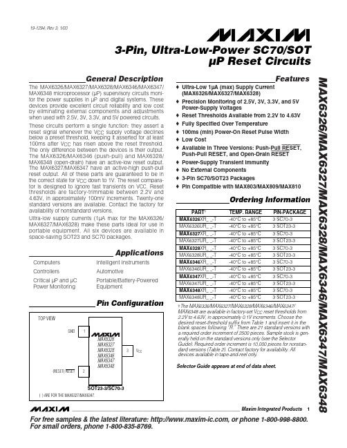
For free samples & the latest literature: , or phone 1-800-998-8800.For small orders, phone 1-800-835-8769.General DescriptionThe MAX6326/MAX6327/MAX6328/MAX6346/MAX6347/MAX6348 microprocessor (µP) supervisory circuits moni-tor the power supplies in µP and digital systems. These devices provide excellent circuit reliability and low cost by eliminating external components and adjustments when used with 2.5V, 3V, 3.3V, and 5V powered circuits.These circuits perform a single function: they assert a reset signal whenever the V CC supply voltage declines below a preset threshold, keeping it asserted for at least 100ms after V CC has risen above the reset threshold.The only difference between the devices is their output.The MAX6326/MAX6346 (push-pull) and MAX6328/MAX6348 (open-drain) have an active-low reset output.The MAX6327/MAX6347 have an active-high push-pull reset output. All of these parts are guaranteed to be in the correct state for V CC down to 1V. The reset compara-tor is designed to ignore fast transients on V CC . Reset thresholds are factory-trimmable between 2.2V and 4.63V, in approximately 100mV increments. Twenty-one standard versions are available. Contact the factory for availability of nonstandard versions.Ultra-low supply currents (1µA max for the MAX6326/MAX6327/MAX6328) make these parts ideal for use in portable equipment. All six devices are available in space-saving SOT23 and SC70 packages.ApplicationsComputers Intelligent Instruments Controllers AutomotiveCritical µP and µC Portable/Battery-Powered Power MonitoringEquipmentFeatureso Ultra-Low 1µA (max) Supply Current (MAX6326/MAX6327/MAX6328)o Precision Monitoring of 2.5V, 3V, 3.3V, and 5V Power-Supply Voltageso Reset Thresholds Available from 2.2V to 4.63V o Fully Specified Over Temperatureo 100ms (min) Power-On Reset Pulse Width o Low Costo Available in Three Versions: Push-Pull RESET ,Push-Pull RESET, and Open-Drain RESET o Power-Supply Transient Immunity o No External Componentso 3-Pin SC70/SOT23 Packageso Pin Compatible with MAX803/MAX809/MAX810MAX6326/MAX6327/MAX6328/MAX6346/MAX6347/MAX63483-Pin, Ultra-Low-Power SC70/SOTµP Reset Circuits________________________________________________________________Maxim Integrated Products 1Pin Configuration19-1294; Rev 3; 1/00†The MAX6326/MAX6327/MAX6328/MAX6346/MAX6347/MAX6348 are available in factory-set V CC reset thresholds from 2.2V to 4.63V, in approximately 0.1V increments. Choose the desired reset-threshold suffix from Table 1 and insert it in the blank spaces following “R.”There are 21 standard versions witha required order increment of 2500 pieces. Sample stock is gen-erally held on the standard versions only (see the SelectorGuide). Required order increment is 10,000 pieces for nonstan-dard versions (Table 2). Contact factory for availability. All devices available in tape-and-reel only.Selector Guide appears at end of data sheet.M A X 6326/M A X 6327/M A X 6328/M A X 6346/M A X 6347/M A X 63483-Pin, Ultra-Low-Power SC70/SOT µP Reset Circuits 2_______________________________________________________________________________________ABSOLUTE MAXIMUM RATINGSELECTRICAL CHARACTERISTICS(V CC = full range, T A = -40°C to +85°C, unless otherwise noted. Typical values are at T A = +25°C and V CC = 3V.) (Note 1)Stresses beyond those listed under “Absolute Maximum Ratings” may cause permanent damage to the device. These are stress ratings only, and functional operation of the device at these or any other conditions beyond those indicated in the operational sections of the specifications is not implied. Exposure to absolute maximum rating conditions for extended periods may affect device reliability.Terminal Voltage (with respect to GND)V CC ...........................................................................-0.3V to +6V RESET, RESET (push-pull).........................-0.3V to (V CC + 0.3V)RESET (open drain)..................................................-0.3V to +6V Input Current (V CC ).............................................................20mA Output Current (RESET, RESET ).........................................20mA Rate of Rise (V CC )...........................................................100V/µsContinuous Power Dissipation (T A = +70°C)3-Pin SC70 (derate 2.7mW/°C above +70°C)...............174mW 3-Pin SOT23 (derate 4mW/°C above +70°C)................320mW Operating Temperature Range ...........................-40°C to +85°C Storage Temperature Range.............................-65°C to +150°C Lead Temperature (soldering, 10s).................................+300°CNote 1:Overtemperature limits are guaranteed by design and not production tested.MAX6326/MAX6327/MAX6328/MAX6346/MAX6347/MAX63483-Pin, Ultra-Low-Power SC70/SOTµP Reset Circuits_______________________________________________________________________________________3__________________________________________Typical Operating Characteristics(T A = +25°C, unless otherwise noted.)00.30.20.10.40.50.60.70.80.91.0-400-2020406080SUPPLY CURRENT vs. TEMPERATURE TEMPERATURE (°C)S U P P L Y C U R R E N T(µA)050100150200-400-2020406080POWER-DOWN RESET DELAY vs. TEMPERATURE TEMPERATURE (°C)R E S E T D E L A Y(µs)130150140160170180190200210-400-2020406080POWER-UP RESET TIMEOUT vs. TEMPERATURE M A X6326-03TEMPERATURE (°C)P O W E R-U P R E S E T T I M E O U T(m s)500011001000MAXIMUM TRANSIENT DURATION vs. RESET THRESHOLD OVERDRIVE (SC70)100300400200M A X6326-04RESET THRESHOLD OVERDRIVE,V TH - V CC (mV)M A X I M U M T R A N S I E N T D U R A T I O N(µs)10______________________________________________________________Pin DescriptionM A X 6326/M A X 6327/M A X 6328/M A X 6346/M A X 6347/M A X 63483-Pin, Ultra-Low-Power SC70/SOT µP Reset Circuits 4___________________________________________________________________________________________________Applications InformationInterfacing to µPs with Bidirectional Reset PinsSince the RESET output on the MAX6328/MAX6348 is open drain, these devices interface easily with micro-processors (µPs) that have bidirectional reset pins,such as the Motorola 68HC11. Connecting the µP supervisor’s RESET output directly to the microcon-troller’s (µC’s) RESET pin with a single pull-up resistor allows either device to assert reset (Figure 1).Negative-Going V CC TransientsIn addition to issuing a reset to the µP during power-up,power-down, and brownout conditions, these devices are relatively immune to short-duration, negative-going V CC transients (glitches).The Typical Operating Characteristics show the Maxi-mum Transient Duration vs. Reset Threshold Overdrive graph, for which reset pulses are not generated. The graph shows the maximum pulse width that a negative-going V CC transient may typically have when issuing a reset signal. As the amplitude of the transient increas-es, the maximum allowable pulse width decreases.Figure 1. Interfacing to µPs with Bidirectional Reset PinsTable 1. Factory-Trimmed Reset Thresholds ‡‡Factory-trimmed reset thresholds are available in approximately 100mV increments with a 1.5% room-temperature variance.MAX6326/MAX6327/MAX6328/MAX6346/MAX6347/MAX63483-Pin, Ultra-Low-Power SC70/SOTµP Reset Circuits_______________________________________________________________________________________5Table 1. Factory-Trimmed Reset Thresholds‡(continued)‡Factory-trimmed reset thresholds are available in approximately 100mV increments with a 1.5% room-temperature variance.Table 2. Device Marking Codes and Minimum Order IncrementsM A X 6326/M A X 6327/M A X 6328/M A X 6346/M A X 6347/M A X 63483-Pin, Ultra-Low-Power SC70/SOT µP Reset Circuits 6__________________________________________________________________________________________________________Chip InformationTRANSISTOR COUNT: 419Table 2. Device Marking Codes and Minimum Order Increments (continued)Selector Guide(standard versions*)*Sample stock is generally held on all standard versions.________________________________________________________Package InformationMAX6326/MAX6327/MAX6328/MAX6346/MAX6347/MAX63483-Pin, Ultra-Low-Power SC70/SOTµP Reset Circuits_______________________________________________________________________________________7M A X 6326/M A X 6327/M A X 6328/M A X 6346/M A X 6347/M A X 63483-Pin, Ultra-Low-Power SC70/SOT µP Reset Circuits Maxim cannot assume responsibility for use of any circuitry other than circuitry entirely embodied in a Maxim product. No circuit patent licenses are implied. Maxim reserves the right to change the circuitry and specifications without notice at any time.8_____________________Maxim Integrated Products, 120 San Gabriel Drive, Sunnyvale, CA 94086 408-737-7600©2000 Maxim Integrated ProductsPrinted USAis a registered trademark of Maxim Integrated Products.Package Information (continued)。
MAX产品后缀说明

MAX 产品后缀说明MAX 产品后缀说明三位后缀例: MAX1675E U A温度范围封装形式管脚数四位后缀另有一些MAXIM 产品后缀用四位表示,第一位表示产品精度等级;第二位表示温度范围:精度,后三位同三位后缀的IC.第三位表示封装形式;第四位表示产品管脚数。
例如:MAX631ACPA 第一个”A”表示5%的输出温度范围C 0°C - 70°C A -40°C - +125°CI -20°C - +85°C M -55 °C - +125°CE -40°C - +85°C封装形式A SSOP(密脚表面贴装)B CERQUAD(陶瓷方形封装)C TO220,TQFP(薄的四方表贴封装)D 陶瓷SB 封装E QSOP(四方表面贴封装)F 陶瓷Flat 封装H 模块SBGA 5*5TQFP J 陶瓷双列直插K SOT L LCCM MQFP(公制四方扁平封装) N 窄体陶瓷双列直插P 塑封DIP(双列直插) Q PLCCR 窄体陶瓷DIP S SO 表面贴封装T TO5,TO99,TO100 U TSSOP,uMAX,SOTV TO39 W 宽体SOX SC70 Y 窄SBZ TO92,MQUAD /D DICE(裸片)/PR 硬塑料/W 晶原管脚数A 8 N 18B 10,64 O 42C 12,192 P 20D 14 Q 2,100E 16 R 3,84F 22,256 S 4,80G 24 T 6,160H 44 U 38,60I 28 V 8(圆脚,隔离型)J 32 W 10(圆脚,隔离型)K 5,68 X 8L 40 Y 8(圆脚,隔离型)M 7,48 Z 10(圆脚,隔离型)。
MAX2335中文资料
Ordering Information
PART
TEMP RANGE PIN-PACKAGE
PKG CODE
MAX2335ETI
-40°C to +85°C
28 Thin QFN-EP* (5mm x 5mm)
T2855-3
MAX2335ETI+ -40°C to +85°C
*EP = Exposed paddle. +Denotes lead-free package.
28-Pin Thin QFN (derate 34.5mW/°C above +70°C) ...........2.7W
Operating Temperature Range ...........................-40°C to +85°C Junction Temperature ......................................................+150°C Storage Temperature Range .............................-65°C to +150°C Lead Temperature (soldering, 10s) .................................+300°C
元器件交易网
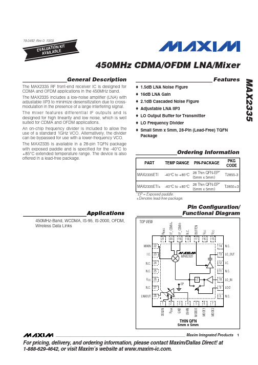
MAX2335
450MHz CDMA/OFDM LNA/Mixer
ABSOLUTE MAXIMUM RATINGS
VCC to GND ...........................................................-0.3V to +4.3V All Other Pins to GND.................................-0.3V to (VCC + 0.3V) AC Input Pins (LNAIN, LO_IN, MIXIN) to GND ...............1V Peak Continuous Power Dissipation (TA = +70°C)
MAX6355TZUT中文资料
For pricing, delivery, and ordering information, please contact Maxim/Dallas Direct! at 1-888-629-4642, or visit Maxim’s website at .
元器件交易网
Features
♦ Precision Monitoring of Multiple +1.8V, +2.5V, +3.0V, +3.3V, and +5V Power-Supply Voltages ♦ Precision Factory-Set Power-Supply Reset Thresholds ♦ 20µA Supply Current ♦ 100ms min Power-On Reset Pulse Width ♦ Debounced TTL/CMOS-Compatible Manual-Reset Input ♦ Watchdog Timer 46.4s Startup Timeout 2.9s Normal Timeout ♦ Fully Guaranteed Over Temperature ♦ Guaranteed RESET Valid to VCC1 = 1V or VCC2 = 1V ♦ Power-Supply Transient Immunity ♦ No External Components for Dual-Voltage Systems ♦ Small 5- and 6-Pin SOT23 Packages ♦ Low Cost
Applications
Computers Controllers Portable/Battery-Powered Equipment Intelligent Instruments Multivoltage Systems
MAX6387XS37D6-T中文资料
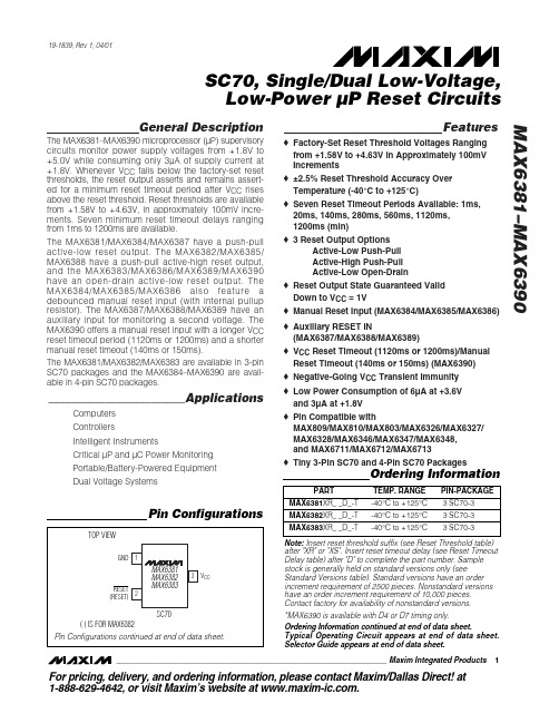
General DescriptionThe MAX6381–MAX6390 microprocessor (µP) supervisory circuits monitor power supply voltages from +1.8V to +5.0V while consuming only 3µA of supply current at +1.8V. Whenever V CC falls below the factory-set reset thresholds, the reset output asserts and remains assert-ed for a minimum reset timeout period after V CC rises above the reset threshold. Reset thresholds are available from +1.58V to +4.63V, in approximately 100mV incre-ments. Seven minimum reset timeout delays ranging from 1ms to 1200ms are available.The MAX6381/MAX6384/MAX6387 have a push-pull active-low reset output. The MAX6382/MAX6385/MAX6388 have a push-pull active-high reset output,and the MAX6383/MAX6386/MAX6389/MAX6390 have an open-drain active-low reset output. The MAX6384/MAX6385/MAX6386 also feature a debounced manual reset input (with internal pullup resistor). The MAX6387/MAX6388/MAX6389 have an auxiliary input for monitoring a second voltage. The MAX6390 offers a manual reset input with a longer V CC reset timeout period (1120ms or 1200ms) and a shorter manual reset timeout (140ms or 150ms).The MAX6381/MAX6382/MAX6383 are available in 3-pin SC70 packages and the MAX6384–MAX6390 are avail-able in 4-pin SC70 packages.________________________ApplicationsComputers ControllersIntelligent InstrumentsCritical µP and µC Power Monitoring Portable/Battery-Powered Equipment Dual Voltage SystemsFeatureso Factory-Set Reset Threshold Voltages Ranging from +1.58V to +4.63V in Approximately 100mV Increments o ±2.5% Reset Threshold Accuracy Over Temperature (-40°C to +125°C)o Seven Reset Timeout Periods Available: 1ms,20ms, 140ms, 280ms, 560ms, 1120ms, 1200ms (min)o 3 Reset Output OptionsActive-Low Push-Pull Active-High Push-Pull Active-Low Open-Draino Reset Output State Guaranteed Valid Down to V CC = 1Vo Manual Reset Input (MAX6384/MAX6385/MAX6386)o Auxiliary RESET IN(MAX6387/MAX6388/MAX6389)o V CC Reset Timeout (1120ms or 1200ms)/Manual Reset Timeout (140ms or 150ms) (MAX6390)o Negative-Going V CC Transient Immunity o Low Power Consumption of 6µA at +3.6V and 3µA at +1.8V o Pin Compatible withMAX809/MAX810/MAX803/MAX6326/MAX6327/MAX6328/MAX6346/MAX6347/MAX6348, and MAX6711/MAX6712/MAX6713o Tiny 3-Pin SC70 and 4-Pin SC70 PackagesMAX6381–MAX6390SC70, Single/Dual Low-Voltage, Low-Power µP Reset Circuits________________________________________________________________Maxim Integrated Products1Pin Configurations19-1839; Rev 1; 04/01Ordering InformationOrdering Information continued at end of data sheet.Typical Operating Circuit appears at end of data sheet.Selector Guide appears at end of data sheet.Note:Insert reset threshold suffix (see Reset Threshold table)after "XR" or "XS". Insert reset timeout delay (see Reset Timeout Delay table) after "D" to complete the part number. Sample stock is generally held on standard versions only (seeStandard Versions table). Standard versions have an order increment requirement of 2500 pieces. Nonstandard versions have an order increment requirement of 10,000 pieces.Contact factory for availability of nonstandard versions.*MAX6390 is available with D4 or D7 timing only.For pricing, delivery, and ordering information,please contact Maxim/Dallas Direct!at 1-888-629-4642, or visit Maxim’s website at .M A X 6381–M A X 6390SC70, Single/Dual Low-Voltage, Low-Power µP Reset CircuitsABSOLUTE MAXIMUM RATINGSELECTRICAL CHARACTERISTICSStresses beyond those listed under “Absolute Maximum Ratings” may cause permanent damage to the device. These are stress ratings only, and functional operation of the device at these or any other conditions beyond those indicated in the operational sections of the specifications is not implied. Exposure to absolute maximum rating conditions for extended periods may affect device reliability.V CC to GND..........................................................-0.3V to +6.0V RESET Open-Drain Output....................................-0.3V to +6.0V RESET , RESET (Push-Pull Output).............-0.3V to (V CC + 0.3V)MR , RESET IN.............................................-0.3V to (V CC + 0.3V)Input Current (V CC ).............................................................20mA Output Current (All Pins).....................................................20mAContinuous Power Dissipation (T A = +70°C)3-Pin SC70 (derate 2.9mW/°C above +70°C)........235mW 4-Pin SC70 (derate 3.1mW/°C above +70°C)........245mW Operating Temperature Range .........................-40°C to +125°C Storage Temperature Range.............................-65°C to +150°C Lead Temperature (soldering, 10s).................................+300°CMAX6381–MAX6390SC70, Single/Dual Low-Voltage, Low-Power µP Reset Circuits_______________________________________________________________________________________3M A X 6381–M A X 6390SC70, Single/Dual Low-Voltage, Low-Power µP Reset Circuits 4______________________________________________________________________________________Typical Operating Characteristics(T A = +25°C, unless otherwise noted.)215436789-40-105-25203550658095110125SUPPLY CURRENT vs. TEMPERATURE(NO LOAD)TEMPERATURE (°C)S U P P L Y C U R R E N T (µA )25292735333137394143-40-105-25203550658095110125POWER-DOWN RESET DELAYvs. TEMPERATURETEMPERATURE (°C)P O W E R -D O W N R E S E T D E L A Y (µs )0.940.980.961.021.001.061.041.08-40-10520-253550658095110125NORMALIZED POWER-UP RESET TIMEOUTvs. TEMPERATUREM A X 6381/90 t o c 03TEMPERATURE (°C)N O R M A L I Z E D R E S E T T I M E O U T P E R I O D0.9900.9851.0150.9950.9901.0001.0051.0101.020-40-10520-253550958011065125M A X 6381/90 t o c 04TEMPERATURE (°C)N O R M A L I Z E D R E S E TT H R E S H O L D NORMALIZED RESET THRESHOLDvs. TEMPERATURE00.40.20.80.61.01.2063912OUTPUT VOLTAGE LOW vs. SINK CURRENTI SINK (mA)V O L (V )01.00.52.01.52.53.00500750250100012501500OUTPUT VOLTAGE HIGH vs. SOURCE CURRENTI SOURCE (µA)V O H (V )45001100010010MAXIMUM TRANSIENT DURATION vs. RESET COMPARATOR OVERDRIVE15050350250500200100400300RESET COMPARATOR OVERDRIVE, V TH - V CC (mV)M A X I M U M T R A N S I E N T D U R A T I O N (µs )3.53.93.74.54.34.14.74.95.35.15.5-40-105-25203550658095110125RESET IN TO RESET DELAYvs. TEMPERATUREM A X 6381/90 t o c 08TEMPERATURE (°C)R E S E T I N D E L A Y (µs )MAX6381–MAX6390SC70, Single/Dual Low-Voltage, Low-Power µP Reset Circuits_______________________________________________________________________________________5M A X 6381–M A X 6390SC70, Single/Dual Low-Voltage, Low-Power µP Reset Circuits 6_______________________________________________________________________________________Detailed DescriptionRESET OutputA µP reset input starts the µP in a known state. These µP supervisory circuits assert reset to prevent code execution errors during power-up, power-down, or brownout conditions.Reset asserts when V CC is below the reset threshold;once V CC exceeds the reset threshold, an internal timer keeps the reset output asserted for the reset timeout period. After this interval, reset output deasserts. Reset output is guaranteed to be in the correct logic state for V CC ≥1V.Manual Reset Input (MAX6384/MAX6385/MAX6386/MAX6390)Many µP-based products require manual reset capabil-ity, allowing the operator, a test technician, or external logic circuitry to initiate a reset. A logic low on MR asserts reset. Reset remains asserted while MR is low,and for the reset active timeout period (t RP ) after MR returns high. This input has an internal 63k Ωpullup resistor (1.35k Ωfor MAX6390), so it can be left uncon-nected if it is not used. MR can be driven with TTL or CMOS logic levels, or with open-drain/collector outputs.Connect a normally open momentary switch from MR to G ND to create a manual-reset function; external debounce circuitry is not required. If MR is driven from long cables or if the device is used in a noisy environ-ment, connecting a 0.1µF capacitor from MR to G ND provides additional noise immunity.RESET IN Comparator(MAX6387/MAX6388/MAX6389)RESET IN is compared to an internal +1.27V reference.If the voltage at RESET IN is less than 1.27V, reset asserts. Use the RESET IN comparator as a user-adjustable reset detector or as a secondary power-sup-ply monitor by implementing a resistor-divider at RESET IN (shown in Figure 1). Reset asserts when either V CC or RESET IN falls below its respective threshold volt-age. Use the following equation to set the threshold:V INTH = V THRST (R1/R2 + 1)where V THRST = +1.27V. To simplify the resistor selec-tion, choose a value of R2 and calculate R1:R1 = R2 [(V INTH /V THRST ) - 1]Since the input current at RESET IN is 50nA (max),large values can be used for R2 with no significant loss in accuracy.___________Applications InformationNegative-Going V CC TransientsIn addition to issuing a reset to the µP during power-up,power-down, and brownout conditions, the MAX6381–MAX6390 are relatively immune to short dura-tion negative-going V CC transients (glitches).The Typical Operating Characteristics section shows the Maximum Transient Durations vs. Reset Comparator Overdrive, for which the MAX6381–MAX6390 do not generate a reset pulse. This graph was generated usinga negative-going pulse applied to V CC , starting above the actual reset threshold and ending below it by the magni-tude indicated (reset comparator overdrive). The graph indicates the typical maximum pulse width a negative-going V CC transient may have without causing a reset pulse to be issued. As the magnitude of the transient increases (goes farther below the reset threshold), the maximum allowable pulse width decreases. A 0.1µF capacitor mounted as close as possible to V CC provides additional transient immunity.Ensuring a Valid RESET Output Down to V CC = 0The MAX6381–MAX6390 are guaranteed to operate properly down to V CC = 1V. In applications that require valid reset levels down to V CC = 0, a pulldown resistor to active-low outputs (push/pull only, Figure 2) and a pullup resistor to active-high outputs (push/pull only) will ensure that the reset line is valid while the reset output can no longer sink or source current. This scheme doesnot work with the open-drain outputs of the MAX6383/MAX6386/MAX6389/MAX6390. The resistor value used is not critical, but it must be small enough not to load the reset output when V CC is above the reset threshold. For most applications, 100k Ωis adequate.MAX6381–MAX6390SC70, Single/Dual Low-Voltage, Low-Power µP Reset Circuits_______________________________________________________________________________________7M A X 6381–M A X 6390SC70, Single/Dual Low-Voltage, Low-Power µP Reset Circuits 8Selector GuideChip InformationTRANSISTOR COUNT: 647PROCESS: BiCMOS*MR is for MAX6384/MAX6385/MAX6386/MAX6390**RESET IN is for MAX6387/MAX6388/MAX6389( ) are for MAX6382/MAX6385/MAX6388Pin Configurations (continued)MAX6381–MAX6390SC70, Single/Dual Low-Voltage, Low-Power µP Reset Circuits_______________________________________________________________________________________9Ordering Information(continued)Note:Insert reset threshold suffix (see Reset Threshold table)after "XR" or "XS". Insert reset timeout delay (see Reset Timeout Delay table) after "D" to complete the part number. Sample stock is generally held on standard versions only (seeStandard Versions table). Standard versions have an order increment requirement of 2500 pieces. Nonstandard versions have an order increment requirement of 10,000 pieces.Contact factory for availability of nonstandard versions.*MAX6390 is available with D4 or D7 timing only.M A X 6381–M A X 6390SC70, Single/Dual Low-Voltage, Low-Power µP Reset Circuits 10______________________________________________________________________________________Package InformationSC70, Single/Dual Low-Voltage, Low-Power µP Reset CircuitsMaxim cannot assume responsibility for use of any circuitry other than circuitry entirely embodied in a Maxim product. No circuit patent licenses are implied. Maxim reserves the right to change the circuitry and specifications without notice at any time.Maxim Integrated Products, 120 San Gabriel Drive, Sunnyvale, CA 94086 408-737-7600____________________11©2001 Maxim Integrated Products Printed USA is a registered trademark of Maxim Integrated Products.MAX6381–MAX6390Package Information (continued)元器件交易网。
1N6375中文资料
1N6373 - 1N6381 Series (ICTE-5 - ICTE-36, MPTE-5 - MPTE-45) 1500 Watt Peak Power Mosorb™ Zener TransientVoltage Suppressors Unidirectional*Mosorb devices are designed to protect voltage sensitive components from high voltage, high–energy transients. They have excellent clamping capability, high surge capability, low zener impedance and fast response time. These devices are ON Semiconductor’s exclusive, cost-effective, highly reliable Surmetic™ axial leaded package and are ideally-suited for use in communication systems, numerical controls, process controls, medical equipment, business machines, power supplies and many other industrial/consumer applications, to protect CMOS, MOS and Bipolar integrated circuits.Specification Features:•Working Peak Reverse V oltage Range – 5 V to 45 V•Peak Power – 1500 Watts @ 1 ms•ESD Rating of Class 3 (>16 KV) per Human Body Model •Maximum Clamp V oltage @ Peak Pulse Current•Low Leakage < 5 m A Above 10 V•Response Time is Typically < 1 nsMechanical Characteristics:CASE:V oid-free, transfer-molded, thermosetting plasticFINISH:All external surfaces are corrosion resistant and leads are readily solderableMAXIMUM LEAD TEMPERATURE FOR SOLDERING PURPOSES: 230°C, 1/16″ from the case for 10 secondsPOLARITY:Cathode indicated by polarity bandMOUNTING POSITION:AnyMAXIMUM RATINGSfor Bidirectional DevicesAXIAL LEADCASE 41APLASTICL = Assembly LocationMPTE–xx = ON Device CodeICTE–xx = ON Device Code1N63xx = JEDEC Device CodeYY = YearWW = Work WeekDevice Package ShippingORDERING INFORMATIONMPTE–xx Axial Lead500 Units/Box MPTE–xxRL4Axial Lead1500/T ape & Reel ICTE–xx Axial Lead500 Units/Box ICTE–xxRL4Axial Lead1500/T ape & ReelNOTES:LICTE–xxYYWW1N63xx Axial Lead500 Units/Box1N63xxRL4*Axial Lead1500/T ape & ReelLMPTE–xx1N63xxYYWW1.Nonrepetitive current pulse per Figure 5 and der-ated above T A = 25°C per Figure 2.2.1/2 sine wave (or equivalent square wave), PW =8.3 ms, duty cycle = 4 pulses per minute maxi-mum.*1N6378 Not Available in 1500/Tape & ReelUni–Directional TVSELECTRICAL CHARACTERISTICS (T A = 25°C unlessotherwise noted, V= 3.5 V Max. @ I (Note 3.) = 100 A)ELECTRICAL CHARACTERISTICS (T= 25°C unless otherwise noted, V = 3.5 V Max. @ I (Note 3.) = 100 A)NOTES:3.Square waveform, PW = 8.3 ms, Non–repetitive duty cycle.4. A transient suppressor is normally selected according to the maximum working peak reverse voltage (V RWM ), which should be equal to or greater than the dc or continuous peak operating voltage level.5.V BR measured at pulse test current I T at an ambient temperature of 25°C and minimum voltage in V BR is to be controlled.6.Surge current waveform per Figure 5 and derate per Figures 1 and 2.*Not Available in the 1500/Tape & ReelFigure 1. Pulse Rating Curve 1008060402000255075100125150175200P E A K P U L S E D E R A T I N G I N % O F P E A K P O W E R O R C U R R E N T @ T A = 25C°T A , AMBIENT TEMPERATURE (°C)Figure 2. Pulse Derating CurveP D , S T E A D Y S T A T E P O W E R D I S S I P A T I O N (W A T T S )T L , LEAD TEMPERATURE (°C)t, TIME (ms)100101t P , PULSE WIDTHP P K, P E A K P O W E R (k W )Figure 3. Capacitance versus Breakdown VoltageFigure 4. Steady State Power Derating Figure 5. Pulse Waveform1N6373, ICTE-5, MPTE-5,through1N6389, ICTE-45,C, MPTE-45,CV BR , BREAKDOWN VOLTAGE (VOLTS)C , C A P A C I T A N C E (p F )1N6373, ICTE-5, MPTE-5,through1N6389, ICTE-45,C, MPTE-45,C1.5KE6.8CA through 1.5KE200CAFigure 6. Dynamic Impedance1000500200100D V BR , INSTANTANEOUS INCREASE IN V BR ABOVE V BR(NOM) (VOLTS)D V BR , INSTANTANEOUS INCREASE IN V BR ABOVE V BR(NOM) (VOLTS)I T , T E S T C U R R E N T (A M P S )Figure 7. Typical Derating Factor for Duty CycleD E R A T I N G F A C T O R10.70.50.30.050.10.010.020.030.07D, DUTY CYCLE (%)APPLICATION NOTESRESPONSE TIMEIn most applications, the transient suppressor device is placed in parallel with the equipment or component to be protected. In this situation, there is a time delay associated with the capacitance of the device and an overshoot condition associated with the inductance of the device and the inductance of the connection method. The capacitance effect is of minor importance in the parallel protection scheme because it only produces a time delay in the transition from the operating voltage to the clamp voltage as shown in Figure 8.The inductive effects in the device are due to actual turn-on time (time required for the device to go from zero current to full current) and lead inductance. This inductive effect produces an overshoot in the voltage across the equipment or component being protected as shown in Figure 9. Minimizing this overshoot is very important in the application, since the main purpose for adding a transient suppressor is to clamp voltage spikes. These devices have excellent response time, typically in the picosecond range and negligible inductance. However, external inductive effects could produce unacceptable overshoot. Proper circuit layout, minimum lead lengths and placing the suppressor device as close as possible to the equipment or components to be protected will minimize this overshoot. Some input impedance represented by Z in is essential to prevent overstress of the protection device. This impedance should be as high as possible, without restricting the circuit operation.DUTY CYCLE DERATINGThe data of Figure 1 applies for non-repetitive conditions and at a lead temperature of 25°C. If the duty cycle increases, the peak power must be reduced as indicated by the curves of Figure 7. Average power must be derated as the lead or ambient temperature rises above 25°C. The average power derating curve normally given on data sheets may be normalized and used for this purpose.At first glance the derating curves of Figure 7 appear to be in error as the 10 ms pulse has a higher derating factor than the 10 m s pulse. However, when the derating factor for a given pulse of Figure 7 is multiplied by the peak power value of Figure 1 for the same pulse, the results follow the expected trend.TYPICAL PROTECTION CIRCUITVFigure 8. Figure 9.OUTLINE DIMENSIONS1500 Watt MosorbTransient Voltage Suppressors – Axial LeadedMOSORB CASE 41A–04ISSUE DDIMA MIN MAX MIN MAX MILLIMETERS0.3350.3748.509.50INCHES B 0.1890.209 4.80 5.30D 0.0380.0420.96 1.06K 1.000---25.40---P---0.050--- 1.27NOTES:1.DIMENSIONING AND TOLERANCING PER ANSI Y14.5M, 1982.2.CONTROLLING DIMENSION: INCH.3.LEAD FINISH AND DIAMETER UNCONTROLLED IN DIMENSION P.4.041A-01 THRU 041A-03 OBSOLETE, NEW STANDARD 041A-04.NotesMosorb and Surmetic are trademarks of Semiconductor Components Industries, LLC.ON Semiconductor and are registered trademarks of Semiconductor Components Industries, LLC (SCILLC). SCILLC reserves the right to make changes without further notice to any products herein. SCILLC makes no warranty, representation or guarantee regarding the suitability of its products for any particular purpose, nor does SCILLC assume any liability arising out of the application or use of any product or circuit, and specifically disclaims any and all liability, including without limitation special, consequential or incidental damages. “Typical” parameters which may be provided in SCILLC data sheets and/or specifications can and do vary in different applications and actual performance may vary over time. All operating parameters, including “Typicals” must be validated for each customer application by customer’s technical experts. SCILLC does not convey any license under its patent rights nor the rights of others.SCILLC products are not designed, intended, or authorized for use as components in systems intended for surgical implant into the body, or other applications intended to support or sustain life, or for any other application in which the failure of the SCILLC product could create a situation where personal injury or death may occur. Should Buyer purchase or use SCILLC products for any such unintended or unauthorized application, Buyer shall indemnify and hold SCILLC and its officers, employees, subsidiaries, affiliates, and distributors harmless against all claims, costs, damages, and expenses, and reasonable attorney fees arising out of, directly or indirectly, any claim of personal injury or death associated with such unintended or unauthorized use, even if such claim alleges that SCILLC was negligent regarding the design or manufacture of the part. SCILLC is an Equal Opportunity/Affirmative Action Employer. PUBLICATION ORDERING INFORMATIONJAPAN: ON Semiconductor, Japan Customer Focus Center4–32–1 Nishi–Gotanda, Shinagawa–ku, Tokyo, Japan 141–0031Phone: 81–3–5740–2700Email: r14525@。
MAX6368PKA23-T中文资料
MAX6365–MAX6368
SOT23, Low-Power µP Supervisory Circuits with Battery Backup and Chip-Enable Gating
ABSOLUTE MAXIMUM RATINGS
Terminal Voltages (with respect to GND)
SOT23 Pin Configurations continued at end of data sheet.
Typical Operating Circuit appears at end of data sheet.
________________________________________________________________ Maxim Integrated Products 1
Pin Configurations
TOP VIEW
RESET, RESET 1 CE IN 2 GND 3 MR 4
MAX6365
8 CE OUT 7 BATT 6 OUT 5 VCC
Features
o Low +1.2V Operating Supply Voltage (VCC or VBATT) o Precision Monitoring of +5.0V, +3.3V, +3.0V, and
VCC, BATT, OUT.......................................................-0.3V to +6V RESET (open drain), RESET (open drain) ................-0.3V to +6V BATT ON, RESET (push-pull), RESET IN,
CY7C63723-PC中文资料
元器件交易网CY7C63743CY7C63722/23CY7C63743enCoRe™ USBCombination Low-Speed USB & PS/2Peripheral ControllerTABLE OF CONTENTS1.0 FEATURES (5)2.0 FUNCTIONAL OVERVIEW (6)2.1 enCoRe USB - The New USB Standard (6)3.0 LOGIC BLOCK DIAGRAM (7)4.0 PIN CONFIGURATIONS (7)5.0 PIN ASSIGNMENTS (7)6.0 PROGRAMMING MODEL (8)6.1 Program Counter (PC) (8)6.2 8-bit Accumulator (A) (8)6.3 8-bit Index Register (X) (8)6.4 8-bit Program Stack Pointer (PSP) (8)6.5 8-bit Data Stack Pointer (DSP) (9)6.6 Address Modes (9)6.6.1 Data (9)6.6.2 Direct (9)6.6.3 Indexed (9)7.0 INSTRUCTION SET SUMMARY (10)8.0 MEMORY ORGANIZATION (11)8.1 Program Memory Organization (11)8.2 Data Memory Organization (12)8.3 I/O Register Summary (13)9.0 CLOCKING (14)9.1 Internal/External Oscillator Operation (15)9.2 External Oscillator (16)10.0 RESET (16)10.1 Low-voltage Reset (LVR) (16)10.2 Brown Out Reset (BOR) (16)10.3 Watchdog Reset (WDR) (17)11.0 SUSPEND MODE (17)11.1 Clocking Mode on Wake-up from Suspend (18)11.2 Wake-up Timer (18)12.0 GENERAL PURPOSE I/O PORTS (18)12.1 Auxiliary Input Port (21)13.0 USB SERIAL INTERFACE ENGINE (SIE) (22)13.1 USB Enumeration (22)13.2 USB Port Status and Control (22)14.0 USB DEVICE (24)14.1 USB Address Register (24)14.2 USB Control Endpoint (24)14.3 USB Non-control Endpoints (25)14.4 USB Endpoint Counter Registers (26)15.0 USB REGULATOR OUTPUT (27)16.0 PS/2 OPERATION (27)17.0 SERIAL PERIPHERAL INTERFACE (SPI) (28)17.1 Operation as an SPI Master (29)17.2 Master SCK Selection (29)17.3 Operation as an SPI Slave (29)17.4 SPI Status and Control (30)17.5 SPI Interrupt (31)17.6 SPI Modes for GPIO Pins (31)18.0 12-BIT FREE-RUNNING TIMER (31)19.0 TIMER CAPTURE REGISTERS (32)20.0 PROCESSOR STATUS AND CONTROL REGISTER (35)21.0 INTERRUPTS (36)21.1 Interrupt Vectors (37)21.2 Interrupt Latency (37)21.3 Interrupt Sources (37)22.0 USB MODE TABLES (42)23.0 REGISTER SUMMARY (47)24.0 ABSOLUTE MAXIMUM RATINGS (48)25.0 DC CHARACTERISTICS (48)26.0 SWITCHING CHARACTERISTICS (50)27.0 ORDERING INFORMATION (55)28.0 PACKAGE DIAGRAMS (55)LIST OF FIGURESFigure 8-1. Program Memory Space with Interrupt Vector Table (11)Figure 8-2. Data Memory Organization (12)Figure 9-1. Clock Oscillator On-chip Circuit (14)Figure 9-2. Clock Configuration Register (Address 0xF8) (14)Figure 10-1. Watchdog Reset (WDR, Address 0x26) (17)Figure 12-1. Block Diagram of GPIO Port (one pin shown) (19)Figure 12-2. Port 0 Data (Address 0x00) (19)Figure 12-3. Port 1 Data (Address 0x01) (19)Figure 12-4. GPIO Port 0 Mode0 Register (Address 0x0A) (20)Figure 12-5. GPIO Port 0 Mode1 Register (Address 0x0B) (20)Figure 12-6. GPIO Port 1 Mode0 Register (Address 0x0C) (20)Figure 12-7. GPIO Port 1 Mode1 Register (Address 0x0D) (20)Figure 12-8. Port 2 Data Register (Address 0x02) (21)Figure 13-1. USB Status and Control Register (Address 0x1F) (23)Figure 14-1. USB Device Address Register (Address 0x10) (24)Figure 14-2. Endpoint 0 Mode Register (Address 0x12) (25)Figure 14-3. USB Endpoint EP1, EP2 Mode Registers (Addresses 0x14 and 0x16) (26)Figure 14-4. Endpoint 0,1,2 Counter Registers (Addresses 0x11, 0x13 and 0x15) (26)Figure 17-1. SPI Block Diagram (28)Figure 16-1. Diagram of USB-PS/2 System Connections (28)Figure 17-2. SPI Data Register (Address 0x60) (29)Figure 17-3. SPI Control Register (Address 0x61) (30)Figure 17-4. SPI Data Timing (31)Figure 18-1. Timer LSB Register (Address 0x24) (31)Figure 18-2. Timer MSB Register (Address 0x25) (32)Figure 18-3. Timer Block Diagram (32)Figure 19-1. Capture Timers Block Diagram (33)Figure 19-2. Capture Timer A-Rising, Data Register (Address 0x40) (33)Figure 19-3. Capture Timer A-Falling, Data Register (Address 0x41) (34)Figure 19-4. Capture Timer B-Rising, Data Register (Address 0x42) (34)Figure 19-5. Capture Timer B-Falling, Data Register (Address 0x43) (34)Figure 19-6. Capture Timer Status Register (Address 0x45) (34)Figure 19-7. Capture Timer Configuration Register (Address 0x44) (34)Figure 20-1. Processor Status and Control Register (Address 0xFF) (35)Figure 21-1. Global Interrupt Enable Register (Address 0x20) (38)Figure 21-2. Endpoint Interrupt Enable Register (Address 0x21) (39)Figure 21-3. Interrupt Controller Logic Block Diagram (40)Figure 21-4. Port 0 Interrupt Enable Register (Address 0x04) (40)Figure 21-5. Port 1 Interrupt Enable Register (Address 0x05) (40)Figure 21-6. Port 0 Interrupt Polarity Register (Address 0x06) (41)Figure 21-7. Port 1 Interrupt Polarity Register (Address 0x07) (41)Figure 21-8. GPIO Interrupt Diagram (41)Figure 26-1. Clock Timing (51)Figure 26-2. USB Data Signal Timing (51)Figure 26-3. Receiver Jitter Tolerance (52)Figure 26-4. Differential to EOP Transition Skew and EOP Width (52)Figure 26-5. Differential Data Jitter (52)Figure 26-7. SPI Slave Timing, CPHA = 0 (53)Figure 26-6. SPI Master Timing, CPHA = 0 (53)Figure 26-8. SPI Master Timing, CPHA = 1 (54)Figure 26-9. SPI Slave Timing, CPHA = 1 (54)LIST OF TABLESTable 8-1. I/O Register Summary (13)Table 11-1. Wake-up Timer Adjust Settings (18)Table 12-1. Ports 0 and 1 Output Control Truth Table (21)Table 13-1. Control Modes to Force D+/D– Outputs (24)Table 17-1. SPI Pin Assignments (31)Table 19-1. Capture Timer Prescalar Settings (Step size and range for FCLK = 6 MHz) (35)Table 21-1. Interrupt Vector Assignments (37)Table 22-1. USB Register Mode Encoding for Control and Non-Control Endpoints (42)Table 22-2. Decode table for Table 22-3: “Details of Modes for Differing Traffic Conditions” (44)Table 22-3. Details of Modes for Differing Traffic Conditions (45)Table 28-1. CY7C63722-XC Probe Pad Coordinates in microns ((0,0) to bond pad centers) (57)1.0 Features•enCoRe™ USB - enhanced Component Reduction—Internal oscillator eliminates the need for an external crystal or resonator—Interface can auto-configure to operate as PS/2 or USB without the need for external components to switch between modes (no GPIO pins needed to manage dual mode capability)—Internal 3.3V regulator for USB pull-up resistor—Configurable GPIO for real-world interface without external components•Flexible, cost-effective solution for applications that combine PS/2 and low-speed USB, such as mice, gamepads, joysticks, and many others.•USB Specification Compliance—Conforms to USB Specification, Version 2.0—Conforms to USB HID Specification, Version 1.1—Supports 1 Low-Speed USB device address and 3 data endpoints—Integrated USB transceiver—3.3V regulated output for USB pull-up resistor•8-bit RISC microcontroller—Harvard architecture—6-MHz external ceramic resonator or internal clock mode—12-MHz internal CPU clock—Internal memory—256 bytes of RAM—8 Kbytes of EPROM—Interface can auto-configure to operate as PS/2 or USB—No external components for switching between PS/2 and USB modes—No GPIO pins needed to manage dual mode capability•I/O ports—Up to 16 versatile General Purpose I/O (GPIO) pins, individually configurable—High current drive on any GPIO pin: 50 mA/pin current sink—Each GPIO pin supports high-impedance inputs, internal pull-ups, open drain outputs or traditional CMOS outputs —Maskable interrupts on all I/O pins•SPI serial communication block—Master or slave operation—2 Mbit/s transfers•Four 8-bit Input Capture registers—Two registers each for two input pins—Capture timer setting with 5 prescaler settings—Separate registers for rising and falling edge capture—Simplifies interface to RF inputs for wireless applications•Internal low-power wake-up timer during suspend mode—Periodic wake-up with no external components•Optional 6-MHz internal oscillator mode—Allows fast start-up from suspend mode•Watchdog Reset (WDR)•Low-voltage Reset at 3.75V•Internal brown-out reset for suspend mode•Improved output drivers to reduce EMI•Operating voltage from 4.0V to 5.5VDC•Operating temperature from 0 to 70 degrees Celsius•CY7C63723 available in 18-pin SOIC, 18-pin PDIP•CY7C63743 available in 24-pin SOIC, 24-pin PDIP•CY7C63722 available in DIE form•Industry standard programmer support2.0 Functional Overview2.1enCoRe USB - The New USB StandardCypress has re-invented its leadership position in the low-speed USB market with a new family of innovative microcontrollers. Introducing...enCoRe USB—“enhanced Component Reduction.” Cypress has leveraged its design expertise in USB solutions to create a new family of low-speed USB microcontrollers that enables peripheral developers to design new products with a minimum number of components. At the heart of the enCoRe USB technology is the breakthrough design of a crystal-less oscillator. By integrating the oscillator into our chip, an external crystal or resonator is no longer needed. We have also integrated other external components commonly found in low-speed USB applications such as pull-up resistors, wake-up circuitry, and a 3.3V regulator. All of this adds up to a lower system cost.The CY7C637xx is an 8-bit RISC One Time Programmable (OTP) microcontroller. The instruction set has been optimized specif-ically for USB and PS/2 operations, although the microcontrollers can be used for a variety of other embedded applications. The CY7C637xx features up to 16 general purpose I/O (GPIO) pins to support USB, PS/2 and other applications. The I/O pins are grouped into two ports (Port 0 to 1) where each pin can be individually configured as inputs with internal pull-ups, open drain outputs, or traditional CMOS outputs with programmable drive strength of up to 50 mA output drive. Additionally, each I/O pin can be used to generate a GPIO interrupt to the microcontroller. Note the GPIO interrupts all share the same “GPIO” interrupt vector. The CY7C637xx microcontrollers feature an internal oscillator. With the presence of USB traffic, the internal oscillator can be set to precisely tune to USB timing requirements (6 MHz ±1.5%). Optionally, an external 6-MHz ceramic resonator can be used to provide a higher precision reference for USB operation. This clock generator reduces the clock-related noise emissions (EMI). The clock generator provides the 6- and 12-MHz clocks that remain internal to the microcontroller.The CY7C637xx has 8 Kbytes of EPROM and 256 bytes of data RAM for stack space, user variables, and USB FIFOs.These parts include low-voltage reset logic, a watchdog timer, a vectored interrupt controller, a 12-bit free-running timer, and capture timers. The low-voltage reset (LVR) logic detects when power is applied to the device, resets the logic to a known state, and begins executing instructions at EPROM address 0x0000. LVR will also reset the part when V CC drops below the operating voltage range. The watchdog timer can be used to ensure the firmware never gets stalled for more than approximately 8 ms. The microcontroller supports 10 maskable interrupts in the vectored interrupt controller. Interrupt sources include the USB Bus-Reset, the 128-µs and 1.024-ms outputs from the free-running timer, three USB endpoints, two capture timers, an internal wake-up timer and the GPIO ports. The timers bits cause periodic interrupts when enabled. The USB endpoints interrupt after USB transactions complete on the bus. The capture timers interrupt whenever a new timer value is saved due to a selected GPIO edge event. The GPIO ports have a level of masking to select which GPIO inputs can cause a GPIO interrupt. For additional flexibility, the input transition polarity that causes an interrupt is programmable for each GPIO pin. The interrupt polarity can be either rising or falling edge.The free-running 12-bit timer clocked at 1 MHz provides two interrupt sources as noted above (128 µs and 1.024 ms). The timer can be used to measure the duration of an event under firmware control by reading the timer at the start and end of an event, and subtracting the two values. The four capture timers save a programmable 8 bit range of the free-running timer when a GPIO edge occurs on the two capture pins (P0.0, P0.1).The CY7C637xx includes an integrated USB serial interface engine (SIE) that supports the integrated peripherals. The hardware supports one USB device address with three endpoints. The SIE allows the USB host to communicate with the function integrated into the microcontroller. A 3.3V regulated output pin provides a pull-up source for the external USB resistor on the D– pin.The USB D+ and D– USB pins can alternately be used as PS/2 SCLK and SDATA signals, so that products can be designed to respond to either USB or PS/2 modes of operation. PS/2 operation is supported with internal pull-up resistors on SCLK and SDATA, the ability to disable the regulator output pin, and an interrupt to signal the start of PS/2 activity. No external components are necessary for dual USB and PS/2 systems, and no GPIO pins need to be dedicated to switching between modes. Slow edge rates operate in both modes to reduce EMI.3.0 Logic Block Diagram4.0 Pin Configurations5.0 Pin AssignmentsNameI/O CY7C63723CY7C63743CY7C63722Description18-Pin 24-Pin 25-Pad D–/SDATA,D+/SCLK I/O 121315161617USB differential data lines (D– and D+), or PS/2 clock and data signals (SDATA and SCLK)P0[7:0]I/O1, 2, 3, 4,15, 16, 17, 181, 2, 3, 4,21, 22, 23, 241, 2, 3, 4,22, 23, 24, 25GPIO Port 0 capable of sinking up to 50 mA/pin, or sinking controlled low or high programmable current.Can also source 2 mA current, provide a resistive pull-up, or serve as a high-impedance input. P0.0 and P0.1 provide inputs to Capture Timers A and B, respec-tively.P1[7:0]I/O5, 145, 6, 7, 8,17, 18, 19, 205, 6, 7, 8,18, 19, 20, 21IO Port 1 capable of sinking up to 50 mA/pin, or sinking controlled low or high programmable current. Can alsosource 2 mA current, provide a resistive pull-up, or serve as a high-impedance input.Wake-Up 12-bit Timer USB &D+,D–P1.0–P1.7Interrupt ControllerPort 0P0.0–P0.7GPIO8-bit RISC Xtal RAM 256 Byte EPROM 8K ByteCoreBrown-out Reset XcvrWatch Timer Dog 3.3V Port 1GPIO Capture TimersUSB Engine PS/2Internal Oscillator Oscillator Low ResetVoltage RegulatorTimerSPIXTALOUTXTALIN/P2.1VREG/P2.01234569111516171819202221P0.0P0.1P0.2P0.3P1.0P1.2VSS VREG/P2.0P0.6P1.5P1.1P1.3D+/SCLK P1.7D–/SDATA VCC14P0.710VPPXTALIN/P2.1XTALOUT121378P1.4P1.62423P0.4P0.524-pin SOIC/PDIPCY7C6374312346781011121315161817P0.0P0.1P0.2P0.3VSS VREG/P2.0P0.4P0.6P0.7D+/SCLK D–/SDATA VCC18-pin SOIC/PDIPP0.59VPPXTALIN/P2.1XTALOUTCY7C63723514P1.0P1.1Top View4 5 6 7 8 93 P 0.21 P 0.0 2 P 0.125 P 0.4 24 P 0.523 P 0.622 21 20 19 1811121314151617P0.3P1.0P1.2P1.4P1.6 VSS VSS V P P X T A L I N /P 2.1V R E G X T A L O U T V C C D -/S D A T A D+/SCLK P0.7P1.1P1.3P1.5P1.7CY7C63722-XCDIE106.0 Programming ModelRefer to the CYASM Assembler User’s Guide for more details on firmware operation with the CY7C637xx microcontrollers.6.1Program Counter (PC)The 14-bit program counter (PC) allows access for up to 8 Kbytes of EPROM using the CY7C637xx architecture. The program counter is cleared during reset, such that the first instruction executed after a reset is at address 0x0000. This instruction is typically a jump instruction to a reset handler that initializes the application.The lower 8 bits of the program counter are incremented as instructions are loaded and executed. The upper 6 bits of the program counter are incremented by executing an XPAGE instruction. As a result, the last instruction executed within a 256-byte “page”of sequential code should be an XPAGE instruction. The assembler directive “XPAGEON” will cause the assembler to insert XPAGE instructions automatically. As instructions can be either one or two bytes long, the assembler may occasionally need to insert a NOP followed by an XPAGE for correct execution.The program counter of the next instruction to be executed, carry flag, and zero flag are saved as two bytes on the program stack during an interrupt acknowledge or a CALL instruction. The program counter, carry flag, and zero flag are restored from the program stack only during a RETI instruction.Please note the program counter cannot be accessed directly by the firmware. The program stack can be examined by reading SRAM from location 0x00 and up.6.28-bit Accumulator (A)The accumulator is the general-purpose, do everything register in the architecture where results are usually calculated.6.38-bit Index Register (X)The index register “X” is available to the firmware as an auxiliary accumulator. The X register also allows the processor to perform indexed operations by loading an index value into X.6.48-bit Program Stack Pointer (PSP)During a reset, the program stack pointer (PSP) is set to zero. This means the program “stack” starts at RAM address 0x00 and “grows” upward from there. Note that the program stack pointer is directly addressable under firmware control, using the MOV PSP ,A instruction. The PSP supports interrupt service under hardware control and CALL, RET, and RETI instructions under firmware control.During an interrupt acknowledge, interrupts are disabled and the program counter, carry flag, and zero flag are written as two bytes of data memory. The first byte is stored in the memory addressed by the program stack pointer, then the PSP is incremented.The second byte is stored in memory addressed by the program stack pointer and the PSP is incremented again. The net effect is to store the program counter and flags on the program “stack” and increment the program stack pointer by two.The return from interrupt (RETI) instruction decrements the program stack pointer, then restores the second byte from memory addressed by the PSP . The program stack pointer is decremented again and the first byte is restored from memory addressed by the PSP . After the program counter and flags have been restored from stack, the interrupts are enabled. The effect is to restore the program counter and flags from the program stack, decrement the program stack pointer by two, and re-enable interrupts.The call subroutine (CALL) instruction stores the program counter and flags on the program stack and increments the PSP by two.XTALIN/P2.1IN 912136-MHz ceramic resonator or external clock input, or P2.1 inputXTALOUT OUT1013146-MHz ceramic resonator return pin or internal oscillator outputV PP 71011Programming voltage supply, ground for normal operation V CC111415Voltage supplyVREG/P2.0 81112Voltage supply for 1.3-k Ω USB pull-up resistor (3.3V nominal). Also serves as P2.0 input.V SS699, 10Ground5.0 Pin Assignments (continued)NameI/O CY7C63723CY7C63743CY7C63722Description18-Pin 24-Pin 25-PadThe return from subroutine (RET) instruction restores the program counter, but not the flags, from program stack and decrements the PSP by two.Note that there are restrictions in using the JMP, CALL, and INDEX instructions across the 4-KB boundary of the program memory. Refer to the CYASM Assembler User’s Guide for a detailed description.6.58-bit Data Stack Pointer (DSP)The data stack pointer (DSP) supports PUSH and POP instructions that use the data stack for temporary storage. A PUSH instruction will pre-decrement the DSP, then write data to the memory location addressed by the DSP. A POP instruction will read data from the memory location addressed by the DSP, then post-increment the DSP.During a reset, the Data Stack Pointer will be set to zero. A PUSH instruction when DSP equals zero will write data at the top of the data RAM (address 0xFF). This would write data to the memory area reserved for a FIFO for USB endpoint 0. In non-USB applications, this works fine and is not a problem.For USB applications, the firmware should set the DSP to an appropriate location to avoid a memory conflict with RAM dedicated to USB FIFOs. The memory requirements for the USB endpoints are shown in Section 8.2. For example, assembly instructions to set the DSP to 20h (giving 32 bytes for program and data stack combined) are shown below:MOV A,20h; Move 20 hex into Accumulator (must be D8h or less to avoid USB FIFOs)SWAP A,DSP; swap accumulator value into DSP register6.6Address ModesThe CY7C637xx microcontrollers support three addressing modes for instructions that require data operands: data, direct, and indexed.6.6.1DataThe “Data” address mode refers to a data operand that is actually a constant encoded in the instruction. As an example, consider the instruction that loads A with the constant 0x30:•MOV A, 30hThis instruction will require two bytes of code where the first byte identifies the “MOV A” instruction with a data operand as the second byte. The second byte of the instruction will be the constant “0xE8h”. A constant may be referred to by name if a prior “EQU” statement assigns the constant value to the name. For example, the following code is equivalent to the example shown above:•DSPINIT: EQU 30h•MOV A,DSPINIT6.6.2Direct“Direct” address mode is used when the data operand is a variable stored in SRAM. In that case, the one byte address of the variable is encoded in the instruction. As an example, consider an instruction that loads A with the contents of memory address location 0x10h:•MOV A, [10h]In normal usage, variable names are assigned to variable addresses using “EQU” statements to improve the readability of the assembler source code. As an example, the following code is equivalent to the example shown above:•buttons: EQU 10h•MOV A,[buttons]6.6.3Indexed“Indexed” address mode allows the firmware to manipulate arrays of data stored in SRAM. The address of the data operand is the sum of a constant encoded in the instruction and the contents of the “X” register. In normal usage, the constant will be the “base” address of an array of data and the X register will contain an index that indicates which element of the array is actually addressed:•array: EQU 10h•MOV X,3•MOV A,[x+array]This would have the effect of loading A with the fourth element of the SRAM “array” that begins at address 0x10h. The fourth element would be at address 0x13h.7.0 Instruction Set SummaryRefer to the CYASM Assembler User’s Guide for detailed information on these instructions. Note that conditional jump instructions (i.e., JC, JNC, JZ, JNZ) take 5 cycles if jump is taken, 4 cycles if no jump.MNEMONIC Operand Opcode Cycles MNEMONIC Operand Opcode Cycles HALT 007NOP 204ADD A,expr data014INC A acc214ADD A,[expr] direct026INC X x224ADD A,[X+expr] index037INC [expr] direct237ADC A,expr data044INC [X+expr] index248ADC A,[expr] direct056DEC A acc254ADC A,[X+expr] index067DEC X x264SUB A,expr data074DEC [expr] direct277SUB A,[expr] direct086DEC [X+expr] index288SUB A,[X+expr] index097IORD expr address295SBB A,expr data0A4IOWR expr address2A5SBB A,[expr] direct0B6POP A2B4SBB A,[X+expr] index0C7POP X2C4OR A,expr data0D4PUSH A2D5OR A,[expr] direct0E6PUSH X2E5OR A,[X+expr] index0F7SWAP A,X2F5AND A,expr data104SWAP A,DSP305AND A,[expr] direct116MOV [expr],A direct315AND A,[X+expr] index127MOV [X+expr],A index326XOR A,expr data134OR [expr],A direct337XOR A,[expr] direct146OR [X+expr],A index348XOR A,[X+expr] index157AND [expr],A direct357CMP A,expr data165AND [X+expr],A index368CMP A,[expr] direct177XOR [expr],A direct377CMP A,[X+expr] index188XOR [X+expr],A index388MOV A,expr data194IOWX [X+expr] index396MOV A,[expr] direct1A5CPL 3A4MOV A,[X+expr] index1B6ASL 3B4MOV X,expr data1C4ASR 3C4MOV X,[expr] direct1D5RLC 3D4reserved 1E RRC 3E4XPAGE 1F4RET 3F8MOV A,X404DI 704MOV X,A414EI 724MOV PSP,A604RETI 738CALL addr50 - 5F10JMP addr80-8F5JC addr C0-CF 5 (or 4) CALL addr90-9F10JNC addr D0-DF 5 (or 4)JZ addr A0-AF 5 (or 4)JACC addr E0-EF7JNZ addr B0-BF 5 (or 4)INDEX addr F0-FF148.0 Memory Organization8.1Program Memory Organization[1]After reset Address14 -bit PC0x0000Program execution begins here after a reset.0x0002USB Bus Reset interrupt vector0x0004128-µs timer interrupt vector0x0006 1.024-ms timer interrupt vector0x0008USB endpoint 0 interrupt vector0x000A USB endpoint 1 interrupt vector0x000C USB endpoint 2 interrupt vector0x000E SPI interrupt vector0x0010Capture timer A interrupt Vector0x0012Capture timer B interrupt vector0x0014GPIO interrupt vector0x0016Wake-up interrupt vector0x0018Program Memory begins here0x1FDF8 KB PROM ends here (8K - 32 bytes). See Note below Figure 8-1. Program Memory Space with Interrupt Vector TableNote:1.The upper 32 bytes of the 8K PROM are reserved. Therefore, the user’s program must not overwrite this space.8.2Data Memory OrganizationThe CY7C637xx microcontrollers provide 256 bytes of data RAM. In normal usage, the SRAM is partitioned into four areas: program stack, data stack, user variables and USB endpoint FIFOs as shown below:After reset Address8-bit DSP8-bit PSP0x00Program Stack Growth(User’s firmware movesDSP)8-bit DSP User Selected Data Stack GrowthUser Variables0xE8USB FIFO for Address A endpoint 20xF0USB FIFO for Address A endpoint 10xF8USB FIFO for Address A endpoint 0Top of RAM Memory0xFFFigure 8-2. Data Memory Organization8.3I/O Register SummaryI/O registers are accessed via the I/O Read (IORD) and I/O Write (IOWR, IOWX) instructions. IORD reads the selected port into the accumulator. IOWR writes data from the accumulator to the selected port. Indexed I/O Write (IOWX) adds the contents of X to the address in the instruction to form the port address and writes data from the accumulator to the specified port. Note that specifying address 0 with IOWX (e.g., IOWX 0h) means the I/O port is selected solely by the contents of X.Note:All bits of all registers are cleared to all zeros on reset, except the Processor Status and Control Register (Figure20-1). All registers not listed are reserved, and should never be written by firmware. All bits marked as reserved should always be written as 0 and be treated as undefined by reads.Table 8-1. I/O Register SummaryRegister Name I/O Address Read/Write Function Fig. Port 0 Data0x00R/W GPIO Port 012-2 Port 1 Data0x01R/W GPIO Port 112-3 Port 2 Data0x02R Auxiliary input register for D+, D–, VREG, XTALIN 12-8 Port 0 Interrupt Enable0x04W Interrupt enable for pins in Port 021-4 Port 1 Interrupt Enable0x05W Interrupt enable for pins in Port 121-5 Port 0 Interrupt Polarity 0x06W Interrupt polarity for pins in Port 021-6 Port 1 Interrupt Polarity 0x07W Interrupt polarity for pins in Port 121-7 Port 0 Mode0 0x0A W Controls output configuration for Port 012-4 Port 0 Mode10x0B W12-5 Port 1 Mode00x0C W Controls output configuration for Port 112-6 Port 1 Mode10x0D W12-7 USB Device Address0x10R/W USB Device Address register14-1 EP0 Counter Register0x11R/W USB Endpoint 0 counter register14-4 EP0 Mode Register0x12R/W USB Endpoint 0 configuration register14-2 EP1 Counter Register0x13R/W USB Endpoint 1 counter register14-4 EP1 Mode Register0x14R/W USB Endpoint 1 configuration register14-3 EP2 Counter Register0x15R/W USB Endpoint 2 counter register14-4 EP2 Mode Register0x16R/W USB Endpoint 2 configuration register14-3 USB Status & Control0x1F R/W USB status and control register13-1 Global Interrupt Enable0x20R/W Global interrupt enable register21-1 Endpoint Interrupt Enable0x21R/W USB endpoint interrupt enables21-2 Timer (LSB)0x24R Lower 8 bits of free-running timer (1 MHz)18-1 Timer (MSB)0x25R Upper 4 bits of free-running timer18-2 WDR Clear0x26W Watchdog Reset clear-Capture Timer A Rising0x40R Rising edge Capture Timer A data register19-2 Capture Timer A Falling0x41R Falling edge Capture Timer A data register19-3 Capture Timer B Rising0x42R Rising edge Capture Timer B data register19-4 Capture Timer B Falling0x43R Falling edge Capture Timer B data register19-5 Capture TImer Configuration0x44R/W Capture Timer configuration register19-7 Capture Timer Status0x45R Capture Timer status register19-6 SPI Data0x60R/W SPI read and write data register17-2 SPI Control0x61R/W SPI status and control register17-3 Clock Configuration0xF8R/W Internal / External Clock configuration register9-2 Processor Status & Control0xFF R/W Processor status and control20-1。
- 1、下载文档前请自行甄别文档内容的完整性,平台不提供额外的编辑、内容补充、找答案等附加服务。
- 2、"仅部分预览"的文档,不可在线预览部分如存在完整性等问题,可反馈申请退款(可完整预览的文档不适用该条件!)。
- 3、如文档侵犯您的权益,请联系客服反馈,我们会尽快为您处理(人工客服工作时间:9:00-18:30)。
General DescriptionThe MAX6375–MAX6380 are ultra-low-power circuits used for monitoring battery, power-supply, and regulat-ed system voltages. Each detector contains a precision bandgap reference, comparator, and internally trimmed resistors that set specified trip threshold voltages.These devices provide excellent circuit reliability and low cost by eliminating external components and adjustments when monitoring nominal system voltages from 2.5V to 5V.These circuits perform a single function: they assert an output signal whenever the V CC supply voltage falls below a preset threshold. The devices are differentiated by their output logic configurations and preset thresh-old voltages. The MAX6375/MAX6378 (push-pull) and MAX6377/MAX6380 (open-drain) have an active-low output (OUT is logic low when V CC is below V TH ). The MAX6376/MAX6379 have an active-high push-pull out-put (OUT is logic high when V CC is below V TH ). All parts are guaranteed to be in the correct output logic state for V CC down to 1V. The detector is designed to ignore fast transients on V CC . The MAX6375/MAX6376/MAX6377 have voltage thresholds between 2.20V and 3.08V in approximately 100mV increments. The MAX6378/MAX6379/MAX6380 have voltage thresholds between 3.30V and 4.63V in approximately 100mV increments.Ultra-low supply current of 500nA (MAX6375/MAX6376/MAX6377) makes these parts ideal for use in portable equipment. All six devices are available in a space-sav-ing SC70 package or in a tiny SOT23 package.ApplicationsPrecision Battery Monitoring Load Switching/Power SequencingPower-Supply Monitoring in Digital/Analog Systems Portable/Battery-Powered EquipmentFeatureso Ultra-Low 500nA Supply Current (MAX6375/MAX6376/MAX6377)o Thresholds Available from 2.20V to 4.63V in Approximately 100mV Incrementso ±2.5% Threshold Accuracy Over Temperature o Low Costo Available in Three Versions: Push-Pull OUT ,Push-Pull OUT, and Open-Drain OUT o Power-Supply Transient Immunity o No External Components o Available in Either a 3-Pin SC70 or 3-Pin SOT23 PackageMAX6375–MAX63803-Pin, Ultra-Low-Power SC70/SOT23Voltage Detectors________________________________________________________________Maxim Integrated Products 1Pin Configuration19-1721; Rev 2; 2/03*The MAX6375/MAX6376/MAX6377 are available in factory-pre-set thresholds from 2.20V to 3.08V, in approximately 0.1V incre-ments. The MAX6378/MAX6379/MAX6380 are available infactory-preset thresholds from 3.30V to 4.63V, in approximately 0.1V increments. Choose the desired threshold suffix fromTable 1 and insert it in the blank spaces following R.There are 21 standard versions, with a required order increment of 2500pieces. Sample stock is generally held on the standard versions only (see the Selector Guide). The required order increment is 10,000 pieces for nonstandard versions (Table 2). Contact facto-ry for availability. All devices available in tape-and-reel only.Selector Guide appears at end of data sheet.For pricing, delivery, and ordering information,please contact Maxim/Dallas Direct!at 1-888-629-4642, or visit Maxim’s website at .Ordering information continued at end of data sheetM A X 6375–M A X 63803-Pin, Ultra-Low-Power SC70/SOT23Voltage Detectors 2_______________________________________________________________________________________ABSOLUTE MAXIMUM RATINGSELECTRICAL CHARACTERISTICS(V CC = full range, T A = -40°C to +85°C, unless otherwise noted. Typical values are at T A = +25°C and V CC = 3V.) (Note 1)Stresses beyond those listed under “Absolute Maximum Ratings” may cause permanent damage to the device. These are stress ratings only, and functional operation of the device at these or any other conditions beyond those indicated in the operational sections of the specifications is not implied. Exposure to absolute maximum rating conditions for extended periods may affect device reliability.Terminal Voltage (with respect to GND)V CC ...........................................................................-0.3V to +6V OUT, OUT (push-pull)................................-0.3V to (V CC + 0.3V)OUT (open-drain).....................................................-0.3V to +6V Input Current (V CC ).............................................................20mA Output Current (OUT, OUT )................................................20mAContinuous Power Dissipation (T A = +70°C)3-Pin SC70 (derate 2.17mW/°C above +70°C)...........174mW 3-Pin SOT23 (derate 4mW/°C above +70°C)..............320mW Operating Temperature Range ...........................-40°C to +85°C Storage Temperature Range.............................-65°C to +150°C Junction Temperature......................................................+150°C Lead Temperature (soldering, 10s).................................+300°CNote 1:Production tested at +25°C only. Overtemperature limits are guaranteed by design, not production tested.MAX6375–MAX63803-Pin, Ultra-Low-Power SC70/SOT23Voltage Detectors__________________________________________Typical Operating Characteristics(V CC = 5V, T A = +25°C, unless otherwise noted.)00.30.20.10.40.50.60.70.80.91.0-40-2020406080SUPPLY CURRENT vs. TEMPERATURETEMPERATURE (°C)S U P P L Y C U R R E N T (µA )050100150200-40-2020406080PROPAGATION DELAY (FALLING)vs. TEMPERATURETEMPERATURE (°C)P R O P A G A T I O N D E L A Y (µs )040208060120100140-4020-20406080PROPAGATION DELAY (RISING)vs. TEMPERATURETEMPERATURE (°C)P R O P A G A T I O N D E L A Y (µs )50011001000MAXIMUM TRANSIENT DURATION vs. THRESHOLD OVERDRIVE100300400200THRESHOLD OVERDRIVEV TH - V CC (mV)M A X I M U M T R A N S I E N T D U R A T I O N (µs )10Pin DescriptionM A X 6375–M A X 63803-Pin, Ultra-Low-Power SC70/SOT23Voltage Detectors____________Applications InformationInterfacing to Different Logic Voltage ComponentsThe MAX6377/MAX6380 have an active-low, open-drain output. This output structure sinks current when OUT is asserted. Connect a pullup resistor from OUT to any supply voltage up to 5.50V (Figure 1). Select a resistor value large enough to allow a valid logic low (see Electrical Characteristics ), and small enough to register a logic high while supplying all input current and leakage paths connected to the OUT line.Negative-Going V CC TransientsThese devices are relatively immune to short-duration,negative-going V CC transients (glitches). The Typical Operating Characteristics show the Maximum Transient Duration vs. Threshold Overdrive graph, for which out-put pulses are not generated. The graph shows the maximum pulse width that a negative-going V CC tran-sient may typically have before the devices issue out-put signals. As the amplitude of the transient increases,the maximum-allowable pulse width decreases.Figure 1. Interfacing to Different Logic Voltage ComponentsTable 1. Factory-Trimmed Reset Thresholds ‡3-Pin, Ultra-Low-Power SC70/SOT23Voltage Detectors_______________________________________________________________________________________5Table 2. Device Marking Codes and Minimum Order IncrementsMAX6375–MAX6380M A X 6375–M A X 63803-Pin, Ultra-Low-Power SC70/SOT23Voltage Detectors 6___________________Chip InformationTRANSISTOR COUNT: 419Selector Guide**S ample stock is generally held on all standard versions.Contact factory for availability of nonstandard versions.Maxim cannot assume responsibility for use of any circuitry other than circuitry entirely embodied in a Maxim product. No circuit patent licenses are implied. Maxim reserves the right to change the circuitry and specifications without notice at any time.Maxim Integrated Products, 120 San Gabriel Drive, Sunnyvale, CA 94086 408-737-7600_____________________7©2003 Maxim Integrated ProductsPrinted USAis a registered trademark of Maxim Integrated Products.3-Pin, Ultra-Low-Power SC70/SOT23Voltage DetectorsMAX6375–MAX6380Package Information(The package drawing(s) in this data sheet may not reflect the most current specifications. For the latest package outline information,go to /packages .)。