1.5KE56中文资料
1.5KE20CA参数资料

POWER: 1500Wa t VOLTAGE RANGE: 6.8 - 440 VAXIAL LEADED TRANSIENT VOLTAGE SUPPRESS DIODE1.5KE6.8A(CA) - 1.5KE440A(CA)6.8V – 440V Standoff VoltageCase: JEDEC DO-201AD Molded Plastic FeaturesGlass Passivated Die Construction Uni- and Bi-Directional Versions Available Excellent Clamping Capability Fast Response TimePlastic Case Material has UL FlammabilityMechanical DataTerminals: Axial Leads, Solderable per MIL-STD-202, Method 208 Polarity: Cathode Band or Cathode Notch Marking:Unidirectional – Device Code and Cathode Band Bidirectional – Device Code OnlyMaximum Ratings and Electrical Characteristics@T A =25°C unless otherwise specifiedCharacteristicSymbol Value Unit Peak Pulse Power Dissipation at T A = 25°C (Note 1, 2, 5) Figure 3P PPM 1500 MinimumW Peak Forward Surge Current (Note 3)I FSM 200A Peak Pulse Current on 10/1000µS Waveform (Note 1) Figure 1I PPM See Table 1A Steady State Power Dissipation (Note 2, 4)P M(AV) 5.0W Operating and Storage Temperature RangeT j , T STG-65 to +175°CNote: 1. Non-repetitive current pulse, per Figure 1 and derated above T A = 25°C per Figure 4.2. Mounted on 40mm 2 copper pad.3. 8.3ms single half sine-wave duty cycle = 4 pulses per minutes maximum.4. Lead temperature at 75°C = T L .5. Peak pulse power waveform is 10/1000µS.!!!!!!!Weight: 1.20 grams (approx.)!森美特94.085.57.0211.4510.513.4 1.5KE440CA1.5KE400CA 1.5KE350A 1.5KE220CA 1.5KE170CA 1.5KE150A 1.5KE82CA (uA)R RMW RMW@V leakage Reverse CurrentPulse Peak (A)Vc(V)(mA)BR MAX CurrentMax.BR MIN @I Min.Volgtage Breakdown (V)(BI)(Uni)Voltage Stand-Off Reverse Maximum Clamping V T PP(V)V @I Volgtage Breakdown Test (V)V T Volgtage @I PP 1.5KE62CA 1.5KE56CA 1.5KE51CA 1.5KE47CA 1.5KE43CA 1.5KE39CA 1.5KE36CA 1.5KE33CA 1.5KE30CA 1.5KE27CA 1.5KE24CA 1.5KE22CA 1.5KE20CA 1.5KE18CA 1.5KE16CA 1.5KE15CA 1.5KE13CA 1.5KE12CA 1.5KE11CA 1.5KE10CA 1.5KE9.1CA 1.5KE8.2CA 1.5KE7.5CA 1.5KE6.8CA 1.5KE6.8A 1.5KE7.5A 1.5KE8.2A 1.5KE9.1A 1.5KE10A 1.5KE11A 1.5KE12A 1.5KE13A 1.5KE15A 1.5KE16A 1.5KE18A 1.5KE20A 1.5KE22A 1.5KE24A 1.5KE27A 1.5KE30A 1.5KE33A1.5KE36A 1.5KE39A 1.5KE43A 1.5KE47A 1.5KE51A 1.5KE56A 1.5KE300CA 1.5KE250CA 1.5KE200CA 1.5KE180CA 1.5KE160CA 1.5KE150CA 1.5KE130CA 1.5KE120CA 1.5KE110CA 1.5KE100CA 1.5KE91CA 1.5KE75CA 1.5KE68CA 1.5KE62A 1.5KE68A 1.5KE75A 1.5KE82A 1.5KE91A 1.5KE100A 1.5KE110A 1.5KE120A 1.5KE130A 1.5KE160A 1.5KE170A 1.5KE180A 1.5KE200A 1.5KE220A 1.5KE250A 1.5KE300A 1.5KE400A 1.5KE440A1.5KE350CA 5.80 6.45 7.14 10 144.8 1000.06.407.13 7.88 10 11.3 134.5 500.0 7.79 8.61 10 12.1 125.6 200.0 7.78 8.65 9.55 1.0 113.4 50.0 8.55 9.50 10.5 1.0 14.5 104.8 10.0 9.40 10.11.6 1.0 15.6 97.4 5.0 10.212.6 1.0 16.7 91.0 5.011.1 12.4 13.7 1.0 18.2 83.5 5.0 12.8 14.3 15.8 1.0 21.2 71.75.013.615.2 16.8 1.0 22.5 67.6 5.0 15.3 17.1 18.9 1.0 25.2 60.3 5.0 17.1 19.0 21.0 1.0 27.7 54.9 5.0 18.820.923.1 1.0 30.6 49.7 5.020.5 22.8 25.2 1.0 33.2 45.8 5.023.1 25.7 28.4 1.0 37.5 40.5 5.0 25.6 28.5 31.5 1.0 41.4 36.7 5.0 28.2 31.4 34.7 1.0 45.7 33.3 5.030.8 34.2 37.8 1.0 49.9 30.5 5.033.3 37.1 41.0 1.0 53.9 28.2 5.0 36.8 40.9 45.2 1.0 59.3 25.6 5.0 40.2 44.7 49.4 1.0 64.8 23.5 5.0 43.648.553.6 1.0 70.1 21.7 5.047.8 53.2 58.8 1.0 77.0 19.7 5.053.0 58.9 65.1 1.0 85.0 17.9 5.058.1 64.6 71.4 1.0 92.0 16.5 5.0 64.1 71.3 78.8 1.0 103 14.8 5.0 70.1 77.9 86.1 1.0 113 13.5 5.0 77.8 86.5 95.5 1.0 125 12.2 5.095.0 105 1.0 137 11.1 5.0105 116 1.0 152 10.0 5.0102 114 126 1.0 165 9.2 5.0 111 124 137 1.0 179 8.5 5.0128 143 158 1.0 207 7.3 5.0136 152 168 1.0 219 6.9 5.0 145 162 179 1.0 234 6.5 5.0 154 171 189 1.0 246 6.2 5.0 171 190 210 1.0 274 5.5 5.0 185 209 231 1.0 328 4.6 5.0 214 237 263 1.0 344 4.4 5.0256 285 315 1.0 414 3.7 5.0300 333 368 1.0 482 3.2 5.0 342 380 420 1.0 548 2.8 5.0 376 418 462 1.0 600 2.5 5.0TYPE森美特255075100125150175200100755025T ,AMBIENT TEMPERATURE (°C)Fig.4Pulse Derating CurveA P K P U L S E D E R A T I N G (%P K P W R O R C U R R E N T )25507510012515017520002.55.0T ,LEAD TEMPERATURE (°C)Fig.5,Steady State Power DeratingLP ,S T E A D Y S T A T E P O W E R D I S S I P A T I O N (W )d 0.11.0T ,PULSE WIDTH (µs)Fig.3Pulse Rating Curvep 0.1101001.010100100010000P ,P E A K P U L S E P O W E R (k W )P0123I ,P E A K P U L S E C U R R E N T (%)P p pt,TIME (ms)Fig.1Pulse Waveform110100100010100100010,000V ,REVERSE STANDOFF VOLTAGE (V)Fig.2Typical Junction CapacitanceRWM C ,C A P A C I T A N C E (p F )j 森美特。
瞬态抑制二极管1.5KE型号参数规格书大全

Axial Lead Transient Voltage Suppressors (TVS)The 1.5KE series is designedspecifically to protect sensitive electronicequipment from voltage transients induced by lightning and other transientvoltage events.Uni-directional Bi-directionalu Glass passivated chip junction in DO-201 Packageu Low leakageu Uni and Bidirectional unitu Excellent clamping capabilityu1500W Peak power capability at 10 × 1000µs waveform Repetitionrate (duty cycle):0.01%u Fast response time: typically less than 1.0ps from 0 Volts to V BR minu Typical I R less than 5μA above 12V.u High Temperature soldering: 260°C/40 seconds at terminalsu Typical maximum temperature coefficient ΔV BR = 0.1% ×V BR@25°C×ΔTu Plastic package has Underwriters Laboratory Flammability 94V-0u Matte tin lead–free Platedu Halogen free and RoHS compliantu Typical failure mode is short from over-specified voltage or currentu Whisker test is conducted based on JEDEC JESD201A per its table4a and 4cu IEC-61000-4-2 ESD 15kV(Air), 8kV (Contact)u ESD protection of data lines in accordance with IEC 61000-4-2(IEC801-2)u EFT protection of data lines in accordance with IEC 61000-4-4(IEC801-4)TVS devices are ideal for the protection of I/O interfaces, V bus and othervulnerable circuits used in Telecom, Computer, Industrial and Consumerelectronic applications.Parameter Symbol Value Unit Peak Pulse Power Dissipation with a 10/1000µs waveform (Fig.1)(Note1), (Note 2)P PPM1500 Watts Peak Pulse Current with a 10/1000µs waveform.(Note1,Fig.3) I PP See Next Table Amps Power Dissipation on Infinite Heat Sink at T L=75°C P M(AV) 6.5 Watt Peak Forward Surge Current, 8.3ms Single Half Sine Wave (Note 3) I FSM200 Amps Maximum Instantaneous Forward Voltage at 25A for Unidirectional Only(Note 4)V F 3.5/5.0 Voltage Operating junction and Storage Temperature Range. T J , T STG-55 to +150 °C Notes:1. Non-repetitive current pulse, per Fig. 3 and derated above T A = 25°C per Fig.2.2. Mounted on 5.0mm x 5.0mm (0.03mm thick) Copper Pads to each terminal.3. 8.3ms single half sine-wave, or equivalent square wave, Duty cycle = 4 pulses per minutes maximum.4. V F < 3.5V for V BR < 200V and V F< 6.5V for V BR > 201V.AAxial Lead Transient Voltage Suppressors (TVS)Part NumberBreakdown Voltage V BR(V)@I T Uni Bi Reverse Stand-Off Voltage V RWM (V) MIN MAX Test Current I T (mA) Maximum Clamping Voltage V C @I PP (V) Maximum Peak Pulse Current I PP (A) Maximum Reverse Leakage I R @V RWM (μA)1.5KE6.8 1.5KE6.8C 5.5 6.12 7.48 10 10.8 138.89 1000 1.5KE6.8A 1.5KE6.8CA 5.8 6.46 7.14 10 10.5 142.86 1000 1.5KE7.5 1.5KE7.5C 6.1 6.75 8.25 10 11.7 128.21 500 1.5KE7.5A 1.5KE7.5CA 6.4 7.13 7.88 10 11.3 132.74 500 1.5KE8.2 1.5KE8.2C 6.6 7.38 9.02 10 12.5 120.00 200 1.5KE8.2A 1.5KE8.2CA 7.0 7.79 8.61 10 12.1 123.97 200 1.5KE9.1 1.5KE9.1C 7.4 8.19 10.01 1 13.8 108.70 50 1.5KE9.1A 1.5KE9.1CA 7.8 8.65 9.56 1 13.4 111.94 50 1.5KE10 1.5KE10C 8.1 9.00 11.00 1 15.0 100.00 10 1.5KE10A 1.5KE10CA 8.6 9.50 10.50 1 14.5 103.45 10 1.5KE11 1.5KE11C 8.9 9.90 12.10 1 16.2 92.59 5 1.5KE11A 1.5KE11CA 9.4 10.45 11.55 1 15.6 96.15 5 1.5KE12 1.5KE12C 9.7 10.80 13.20 1 17.3 86.71 5 1.5KE12A 1.5KE12CA 10.2 11.40 12.60 1 16.7 89.82 5 1.5KE13 1.5KE13C 10.5 11.70 14.30 1 19.0 78.95 5 1.5KE13A 1.5KE13CA 11.1 12.35 13.65 1 18.2 82.42 5 1.5KE15 1.5KE15C 12.1 13.50 16.50 1 22.0 68.18 5 1.5KE15A 1.5KE15CA 12.8 14.25 15.75 1 21.2 70.75 5 1.5KE16 1.5KE16C 12.9 14.40 17.60 1 23.5 63.83 5 1.5KE16A 1.5KE16CA 13.6 15.20 16.80 1 22.5 66.67 5 1.5KE18 1.5KE18C 14.5 16.20 19.80 1 26.5 56.60 5 1.5KE18A 1.5KE18CA 15.3 17.10 18.90 1 25.2 59.52 5 1.5KE20 1.5KE20C 16.2 18.00 22.00 1 29.1 51.55 5 1.5KE20A 1.5KE20CA 17.1 19.00 21.00 1 27.7 54.15 5 1.5KE22 1.5KE22C 17.8 19.80 24.20 1 31.9 47.02 5 1.5KE22A 1.5KE22CA 18.8 20.90 23.10 1 30.6 49.02 5 1.5KE24 1.5KE24C 19.4 21.60 26.40 1 34.7 43.23 5 1.5KE24A 1.5KE24CA 20.5 22.80 25.20 1 33.2 45.18 5 1.5KE27 1.5KE27C 21.8 24.30 29.70 1 39.1 38.36 5 1.5KE27A 1.5KE27CA 23.1 25.65 28.35 1 37.5 40.00 5 1.5KE30 1.5KE30C 24.3 27.00 33.00 1 43.5 34.48 5 1.5KE30A 1.5KE30CA 25.6 28.50 31.50 1 41.4 36.23 5 1.5KE33 1.5KE33C 26.8 29.70 36.30 1 47.7 31.45 5 1.5KE33A 1.5KE33CA 28.2 31.35 34.65 1 45.7 32.82 5 1.5KE36 1.5KE36C 29.1 32.40 39.60 1 52.0 28.85 5 1.5KE36A 1.5KE36CA 30.8 34.20 37.80 1 49.9 30.06 5 1.5KE39 1.5KE39C 31.6 35.10 42.90 1 56.4 36.60 5 1.5KE39A 1.5KE39CA 33.3 37.05 40.95 1 53.9 27.83 5 1.5KE43 1.5KE43C 34.8 38.70 47.30 1 61.9 24.23 5 1.5KE43A 1.5KE43CA 36.8 40.85 45.15 1 59.3 25.30 5 1.5KE47 1.5KE47C 38.1 42.30 51.70 1 67.8 22.12 5 1.5KE47A 1.5KE47CA 40.2 44.65 49.35 1 64.8 23.15 5 1.5KE51 1.5KE51C 41.3 45.90 56.10 1 73.5 20.41 5 1.5KE51A 1.5KE51CA 43.6 48.45 53.55 1 70.1 21.40 5 1.5KE56 1.5KE56C 45.4 50.40 61.60 1 80.5 18.63 5 1.5KE56A 1.5KE56CA 47.8 53.20 58.80 1 77.0 19.48 5 1.5KE62 1.5KE62C 50.2 55.80 68.20 1 89.0 16.85 5 1.5KE62A 1.5KE62CA 53.0 58.90 65.10 1 85.0 17.65 5 1.5KE68 1.5KE68C 55.1 61.20 74.80 1 98.0 15.31 5 1.5KE68A 1.5KE68CA 58.1 64.60 71.40 1 92.0 16.30 5 1.5KE75 1.5KE75C 60.7 67.50 82.50 1 108.0 13.89 5 1.5KE75A 1.5KE75CA 64.1 71.25 78.75 1 103.0 14.56 5 1.5KE82 1.5KE82C 66.4 73.80 90.20 1 118.0 12.71 5 1.5KE82A1.5KE82CA70.177.9086.101113.013.275AAxial Lead Transient Voltage Suppressors (TVS)Part Number Breakdown Voltage V BR(V)@I T UniBi Reverse Stand-Off Voltage V RWM (V) MIN MAX Test Current I T (mA)Maximum Clamping Voltage V C @I PP (V) Maximum Peak Pulse Current I PP (A) Maximum Reverse Leakage I R @V RWM (μA)1.5KE91 1.5KE91C 73.7 81.90 100.10 1 131.0 11.45 5 1.5KE91A 1.5KE91CA 77.8 86.45 95.55 1 125.0 12.00 5 1.5KE100 1.5KE100C 81.0 90.00 110.00 1 144.0 10.42 5 1.5KE100A 1.5KE100CA 85.5 95.00 105.00 1 137.0 10.95 5 1.5KE110 1.5KE110C 89.2 99.00 121.00 1 158.0 9.49 5 1.5KE110A 1.5KE110CA 94.0 104.50 115.50 1 152.0 9.87 5 1.5KE120 1.5KE120C 97.2 108.00 132.00 1 173.0 8.67 5 1.5KE120A 1.5KE120CA 102.0 114.00 126.00 1 165.0 9.09 5 1.5KE130 1.5KE130C 105.0 117.00 143.00 1 187.0 8.02 5 1.5KE130A 1.5KE130CA 111.0 123.50 136.50 1 179.0 8.38 5 1.5KE150 1.5KE150C 121.0 135.00 165.00 1 215.0 6.98 5 1.5KE150A 1.5KE150CA 128.0 142.50 157.50 1 207.0 7.25 5 1.5KE160 1.5KE160C 130.0 144.00 176.00 1 230.0 6.52 5 1.5KE160A 1.5KE160CA 136.0 152.00 168.00 1 219.0 6.85 5 1.5KE170 1.5KE170C 138.0 153.00 187.00 1 244.0 6.15 5 1.5KE170A 1.5KE170CA 145.0 161.50 178.50 1 234.0 6.41 5 1.5KE180 1.5KE180C 146.0 162.00 198.00 1 258.0 5.81 5 1.5KE180A 1.5KE180CA 154.0 171.00 189.00 1 246.0 6.10 5 1.5KE200 1.5KE200C 162.0 180.00 220.00 1 287.0 5.23 5 1.5KE200A 1.5KE200CA 171.0 190.00 210.00 1 274.0 5.47 5 1.5KE220 1.5KE220C 175.0 198.00 242.00 1 344.0 4.36 5 1.5KE220A 1.5KE220CA 185.0 209.00 231.00 1 328.0 4.57 5 1.5KE250 1.5KE250C 202.0 225.00 275.00 1 360.0 4.17 5 1.5KE250A 1.5KE250CA 214.0 237.50 262.50 1 344.0 4.36 5 1.5KE300 1.5KE300C 243.0 270.00 330.00 1 430.0 3.49 5 1.5KE300A 1.5KE300CA 256.0 285.00 315.00 1 414.0 3.62 5 1.5KE350 1.5KE350C 284.0 315.00 385.00 1 504.0 2.98 5 1.5KE350A 1.5KE350CA 299.3 332.50 367.50 1 482.0 3.11 5 1.5KE380 1.5KE380C 308.6 342.00 418.00 1 547.2 2.74 5 1.5KE380A 1.5KE380CA 324.9 361.00 399.00 1 524.4 2.86 5 1.5KE400 1.5KE400C 324.8 360.00 440.00 1 576.0 2.60 5 1.5KE400A 1.5KE400CA 342.0 380.00 420.00 1 552.0 2.72 5 1.5KE440 1.5KE440C 357.3 396.00 484.00 1 633.6 2.37 5 1.5KE440A 1.5KE440CA 376.2 418.00 462.00 1 607.2 2.47 5 1.5KE500 1.5KE500C 406.0 450.00 550.00 1 720.0 2.08 5 1.5KE500A 1.5KE500CA 427.5 475.00 525.00 1 690.0 2.17 5 1.5KE520 1.5KE520C 422.2 468.00 572.00 1 748.8 2.00 5 1.5KE520A 1.5KE520CA 444.6 494.00 546.00 1 717.6 2.09 5 1.5KE550 1.5KE550C 446.6 495.00 605.00 1 792.0 1.89 5 1.5KE550A 1.5KE550CA 470.3 522.50 577.50 1 759.0 1.98 5 1.5KE600 1.5KE600C 487.2 540.00 660.00 1 864.0 1.74 5 1.5KE600A 1.5KE600CA513.0570.00630.001 828.01.815Note:1. Suffix 'A ' denotes 5% tolerance device. Without 'A' denotes 10% tolerance device2. Add suffix 'C 'or ' CA ' after part number to specify Bi-directional devices3. For Bi-Directional devices having V R of 10 volts and under, the I R limit is doubleAATemperature Cycle JESD22-A104 Weight 0.032 ounce, 0.9 gramPressure Cooker JESD22-A102 Case JEDEC DO-201 Molded Plastic over glass passivated junctionHigh Temp. Storage JESD22-A103 Polarity Color band denotes cathode except BipolarHTRBJESD22-A108 TerminalMatte Tin-plated leads, Solderable per JESD22-B102DThermal ShockJESD22-A106Reflow ConditionLead –free assembly -Temperature Min (T s(min))150°C -Temperature Max (T s(max)) 200°CPre Heat- Time (min to max) (t s )60 -180 Seconds Average ramp up rate ( Liquidus Temp T L ) to peak3°C/second max T S(max) to TL - Ramp-up Rate3°C/second max - Temperature (T L ) (Liquidus) 217°CReflow- Time (min to max) (t s )60 -150 SecondsPeak Temperature (T P ) 260 +0/-5°CTime within 5°C ofactualpeakTemperature (t p )20 -40 Seconds Ramp-down Rate6°C/second max Time 25°C to peak Temperature (T P ) 8 minutes MaxDo not exceed280°CRamp-down PreheatTime to peak temperature(t 25℃ to peak)Ramp-upTime Physical SpecificationsEnvironmental SpecificationsSoldering Parameters。
1.5KE16CA,TVS瞬变二极管中文资料
POWER: 1500Wa t VOLTAGE RANGE: 6.8 - 440 VAXIAL LEADED TRANSIENT VOLTAGE SUPPRESS DIODE1.5KE6.8A(CA) - 1.5KE440A(CA)6.8V – 440V Standoff VoltageCase: JEDEC DO-201AD Molded Plastic FeaturesGlass Passivated Die Construction Uni- and Bi-Directional Versions Available Excellent Clamping Capability Fast Response TimePlastic Case Material has UL FlammabilityMechanical DataTerminals: Axial Leads, Solderable per MIL-STD-202, Method 208 Polarity: Cathode Band or Cathode Notch Marking:Unidirectional – Device Code and Cathode Band Bidirectional – Device Code OnlyMaximum Ratings and Electrical Characteristics@T A =25°C unless otherwise specifiedCharacteristicSymbol ValueUnit Peak Pulse Power Dissipation at T A = 25°C (Note 1, 2, 5) Figure 3P PPM 1500 MinimumW Peak Forward Surge Current (Note 3)I FSM 200A Peak Pulse Current on 10/1000µS Waveform (Note 1) Figure 1I PPM See Table 1A Steady State Power Dissipation (Note 2, 4)P M(AV) 5.0W Operating and Storage Temperature RangeT j , T STG-65 to +175°CNote: 1. Non-repetitive current pulse, per Figure 1 and derated above T A = 25°C per Figure 4.2. Mounted on 40mm 2 copper pad.3. 8.3ms single half sine-wave duty cycle = 4 pulses per minutes maximum.4. Lead temperature at 75°C = T L .5. Peak pulse power waveform is 10/1000µS.!!!!!!!Weight: 1.20 grams (approx.)!94.085.57.0211.4510.513.4 1.5KE440CA1.5KE400CA 1.5KE350A 1.5KE220CA 1.5KE170CA 1.5KE150A 1.5KE82CA (uA)R RMW RMW@V leakage Reverse CurrentPulse Peak (A)Vc(V)(mA)BR MAX CurrentMax.BR MIN @I Min.Volgtage Breakdown (V)(BI)(Uni)Voltage Stand-Off Reverse Maximum Clamping V T PP(V)V @I Volgtage Breakdown Test (V)V T Volgtage @I PP 1.5KE62CA 1.5KE56CA 1.5KE51CA 1.5KE47CA 1.5KE43CA 1.5KE39CA 1.5KE36CA 1.5KE33CA 1.5KE30CA 1.5KE27CA 1.5KE24CA 1.5KE22CA 1.5KE20CA 1.5KE18CA 1.5KE16CA 1.5KE15CA 1.5KE13CA 1.5KE12CA 1.5KE11CA 1.5KE10CA 1.5KE9.1CA 1.5KE8.2CA 1.5KE7.5CA 1.5KE6.8CA 1.5KE6.8A 1.5KE7.5A 1.5KE8.2A 1.5KE9.1A 1.5KE10A 1.5KE11A 1.5KE12A 1.5KE13A 1.5KE15A 1.5KE16A 1.5KE18A 1.5KE20A 1.5KE22A 1.5KE24A 1.5KE27A 1.5KE30A 1.5KE33A 1.5KE36A 1.5KE39A1.5KE43A 1.5KE47A 1.5KE51A 1.5KE56A 1.5KE300CA 1.5KE250CA 1.5KE200CA 1.5KE180CA 1.5KE160CA 1.5KE150CA 1.5KE130CA 1.5KE120CA 1.5KE110CA 1.5KE100CA 1.5KE91CA 1.5KE75CA 1.5KE68CA 1.5KE62A 1.5KE68A 1.5KE75A 1.5KE82A 1.5KE91A 1.5KE100A 1.5KE110A 1.5KE120A 1.5KE130A 1.5KE160A 1.5KE170A 1.5KE180A 1.5KE200A 1.5KE220A 1.5KE250A 1.5KE300A 1.5KE400A 1.5KE440A1.5KE350CA 5.80 6.45 7.14 10 144.8 1000.06.407.13 7.88 10 11.3 134.5 500.0 7.79 8.61 10 12.1 125.6 200.0 7.78 8.65 9.55 1.0 113.4 50.0 8.55 9.50 10.5 1.0 14.5 104.8 10.0 9.40 10.11.6 1.0 15.6 97.4 5.0 10.212.6 1.0 16.7 91.0 5.011.1 12.4 13.7 1.0 18.2 83.5 5.0 12.8 14.3 15.8 1.0 21.2 71.75.013.615.2 16.8 1.0 22.5 67.6 5.0 15.3 17.1 18.9 1.0 25.2 60.3 5.0 17.1 19.0 21.0 1.0 27.7 54.9 5.0 18.820.923.1 1.0 30.6 49.7 5.020.5 22.8 25.2 1.0 33.2 45.8 5.023.1 25.7 28.4 1.0 37.5 40.5 5.0 25.6 28.5 31.5 1.0 41.4 36.7 5.0 28.2 31.4 34.7 1.0 45.7 33.3 5.030.8 34.2 37.8 1.0 49.9 30.5 5.033.3 37.1 41.0 1.0 53.9 28.2 5.0 36.8 40.9 45.2 1.0 59.3 25.6 5.0 40.2 44.7 49.4 1.0 64.8 23.5 5.0 43.648.553.6 1.0 70.1 21.7 5.047.8 53.2 58.8 1.0 77.0 19.7 5.053.0 58.9 65.1 1.0 85.0 17.9 5.058.1 64.6 71.4 1.0 92.0 16.5 5.0 64.1 71.3 78.8 1.0 103 14.8 5.0 70.1 77.9 86.1 1.0 113 13.5 5.0 77.8 86.5 95.5 1.0 125 12.2 5.095.0 105 1.0 137 11.1 5.0105 116 1.0 152 10.0 5.0102 114 126 1.0 165 9.2 5.0 111 124 137 1.0 179 8.5 5.0128 143 158 1.0 207 7.3 5.0136 152 168 1.0 219 6.9 5.0 145 162 179 1.0 234 6.5 5.0 154 171 189 1.0 246 6.2 5.0 171 190 210 1.0 274 5.5 5.0 185 209 231 1.0 328 4.6 5.0 214 237 263 1.0 344 4.4 5.0256 285 315 1.0 414 3.7 5.0300 333 368 1.0 482 3.2 5.0 342 380 420 1.0 548 2.8 5.0 376 418 462 1.0 600 2.5 5.0TYPE255075100125150175200100755025T ,AMBIENT TEMPERATURE (°C)Fig.4Pulse Derating CurveA P K P U L S E D E R A T I N G (%P K P W R O R C U R R E N T )25507510012515017520002.55.0T ,LEAD TEMPERATURE (°C)Fig.5,Steady State Power DeratingLP ,S T E A D Y S T A T E P O W E R D I S S I P A T I O N (W )d 0.11.0T ,PULSE WIDTH (µs)Fig.3Pulse Rating Curvep 0.1101001.010100100010000P ,P E A K P U L S E P O W E R (k W )P 0123I ,P E A K P U L S E C U R R E N T (%)P p pt,TIME (ms)Fig.1Pulse Waveform110100100010100100010,000V ,REVERSE STANDOFF VOLTAGE (V)Fig.2Typical Junction CapacitanceRWM C ,C A P A C I T A N C E (p F )j。
1.5KE6.8CA参数资料

POWER: 1500Wa t VOLTAGE RANGE: 6.8 - 440 VAXIAL LEADED TRANSIENT VOLTAGE SUPPRESS DIODE1.5KE6.8A(CA) - 1.5KE440A(CA)6.8V – 440V Standoff VoltageCase: JEDEC DO-201AD Molded Plastic FeaturesGlass Passivated Die Construction Uni- and Bi-Directional Versions Available Excellent Clamping Capability Fast Response TimePlastic Case Material has UL FlammabilityMechanical DataTerminals: Axial Leads, Solderable per MIL-STD-202, Method 208 Polarity: Cathode Band or Cathode Notch Marking:Unidirectional – Device Code and Cathode Band Bidirectional – Device Code OnlyMaximum Ratings and Electrical Characteristics@T A =25°C unless otherwise specifiedCharacteristicSymbol Value Unit Peak Pulse Power Dissipation at T A = 25°C (Note 1, 2, 5) Figure 3P PPM 1500 MinimumW Peak Forward Surge Current (Note 3)I FSM 200A Peak Pulse Current on 10/1000µS Waveform (Note 1) Figure 1I PPM See Table 1A Steady State Power Dissipation (Note 2, 4)P M(AV) 5.0W Operating and Storage Temperature RangeT j , T STG-65 to +175°CNote: 1. Non-repetitive current pulse, per Figure 1 and derated above T A = 25°C per Figure 4.2. Mounted on 40mm 2 copper pad.3. 8.3ms single half sine-wave duty cycle = 4 pulses per minutes maximum.4. Lead temperature at 75°C = T L .5. Peak pulse power waveform is 10/1000µS.!!!!!!!Weight: 1.20 grams (approx.)!森美特1.5KE6.8CA94.085.57.0211.4510.513.4 1.5KE440CA1.5KE400CA 1.5KE350A 1.5KE220CA 1.5KE170CA 1.5KE150A 1.5KE82CA (uA)R RMW RMW@V leakage Reverse CurrentPulse Peak (A)Vc(V)(mA)BR MAX CurrentMax.BR MIN @I Min.Volgtage Breakdown (V)(BI)(Uni)Voltage Stand-Off Reverse Maximum Clamping V T PP(V)V @I Volgtage Breakdown Test (V)V T Volgtage @I PP 1.5KE62CA 1.5KE56CA 1.5KE51CA 1.5KE47CA 1.5KE43CA 1.5KE39CA 1.5KE36CA 1.5KE33CA 1.5KE30CA 1.5KE27CA 1.5KE24CA 1.5KE22CA 1.5KE20CA 1.5KE18CA 1.5KE16CA 1.5KE15CA 1.5KE13CA 1.5KE12CA 1.5KE11CA 1.5KE10CA 1.5KE9.1CA 1.5KE8.2CA 1.5KE7.5CA 1.5KE6.8A 1.5KE7.5A 1.5KE8.2A 1.5KE9.1A 1.5KE10A 1.5KE11A 1.5KE12A 1.5KE13A 1.5KE15A 1.5KE16A 1.5KE18A 1.5KE20A 1.5KE22A 1.5KE24A 1.5KE27A 1.5KE30A 1.5KE33A 1.5KE36A1.5KE39A 1.5KE43A 1.5KE47A 1.5KE51A 1.5KE56A 1.5KE300CA 1.5KE250CA 1.5KE200CA 1.5KE180CA 1.5KE160CA 1.5KE150CA 1.5KE130CA 1.5KE120CA 1.5KE110CA 1.5KE100CA 1.5KE91CA 1.5KE75CA 1.5KE68CA 1.5KE62A 1.5KE68A 1.5KE75A 1.5KE82A 1.5KE91A 1.5KE100A 1.5KE110A 1.5KE120A 1.5KE130A 1.5KE160A 1.5KE170A 1.5KE180A 1.5KE200A 1.5KE220A 1.5KE250A 1.5KE300A 1.5KE400A 1.5KE440A1.5KE350CA 5.80 6.45 7.14 10 144.8 1000.06.407.13 7.88 10 11.3 134.5 500.0 7.79 8.61 10 12.1 125.6 200.0 7.78 8.65 9.55 1.0 113.4 50.0 8.55 9.50 10.5 1.0 14.5 104.8 10.0 9.40 10.11.6 1.0 15.6 97.4 5.0 10.212.6 1.0 16.7 91.0 5.011.1 12.4 13.7 1.0 18.2 83.5 5.0 12.8 14.3 15.8 1.0 21.2 71.75.013.615.2 16.8 1.0 22.5 67.6 5.0 15.3 17.1 18.9 1.0 25.2 60.3 5.0 17.1 19.0 21.0 1.0 27.7 54.9 5.0 18.820.923.1 1.0 30.6 49.7 5.020.5 22.8 25.2 1.0 33.2 45.8 5.023.1 25.7 28.4 1.0 37.5 40.5 5.0 25.6 28.5 31.5 1.0 41.4 36.7 5.0 28.2 31.4 34.7 1.0 45.7 33.3 5.030.8 34.2 37.8 1.0 49.9 30.5 5.033.3 37.1 41.0 1.0 53.9 28.2 5.0 36.8 40.9 45.2 1.0 59.3 25.6 5.0 40.2 44.7 49.4 1.0 64.8 23.5 5.0 43.648.553.6 1.0 70.1 21.7 5.047.8 53.2 58.8 1.0 77.0 19.7 5.053.0 58.9 65.1 1.0 85.0 17.9 5.058.1 64.6 71.4 1.0 92.0 16.5 5.0 64.1 71.3 78.8 1.0 103 14.8 5.0 70.1 77.9 86.1 1.0 113 13.5 5.0 77.8 86.5 95.5 1.0 125 12.2 5.095.0 105 1.0 137 11.1 5.0105 116 1.0 152 10.0 5.0102 114 126 1.0 165 9.2 5.0 111 124 137 1.0 179 8.5 5.0128 143 158 1.0 207 7.3 5.0136 152 168 1.0 219 6.9 5.0 145 162 179 1.0 234 6.5 5.0 154 171 189 1.0 246 6.2 5.0 171 190 210 1.0 274 5.5 5.0 185 209 231 1.0 328 4.6 5.0 214 237 263 1.0 344 4.4 5.0256 285 315 1.0 414 3.7 5.0300 333 368 1.0 482 3.2 5.0 342 380 420 1.0 548 2.8 5.0 376 418 462 1.0 600 2.5 5.0TYPE森美特1.5KE6.8CA255075100125150175200100755025T ,AMBIENT TEMPERATURE (°C)Fig.4Pulse Derating CurveA P K P U L S E D E R A T I N G (%P K P W R O R C U R R E N T )25507510012515017520002.55.0T ,LEAD TEMPERATURE (°C)Fig.5,Steady State Power DeratingLP ,S T E A D Y S T A T E P O W E R D I S S I P A T I O N (W )d 0.11.0T ,PULSE WIDTH (µs)Fig.3Pulse Rating Curvep 0.1101001.010100100010000P ,P E A K P U L S E P O W E R (k W )P0123I ,P E A K P U L S E C U R R E N T (%)P p pt,TIME (ms)Fig.1Pulse Waveform110100100010100100010,000V ,REVERSE STANDOFF VOLTAGE (V)Fig.2Typical Junction CapacitanceRWM C ,C A P A C I T A N C E (p F )j 森美特。
1.5KE43CA(SynSemi)中文数据手册「EasyDatasheet」
P,D稳态功耗0 0
25
50 75 100 125 150 175 200
TL,引线温度(℃)
图5 -脉冲波形
RMS Tr = 10µs
100
Peak Value
IRMS
TJ=25 °C Pulse Width (tp) is defined as that point where the peak current decays to 50% of IRSM
94.0
1.5KE120A 1.5KE120CA
114
126
1.0
102
1.5KE130A 1.5KE130CA
124
137
1.0
111
1.5KE150A 1.5KE150CA
143
158
1.0
128
1.5KE160A 1.5KE160CA
152
168
1.0
136
1.5KE170A 1.5KE170CA
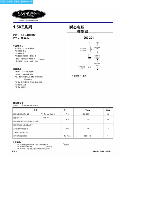
瞬态电压 抑制器
DO-201
0.21 (5.33) 0.19 (4.83)
0.052 (1.07) 0.048 (0.97)
1.00 (25.4) MIN.
0.375 (9.53) 0.285 (7.24)
1.00 (25.4) MIN.
尺寸以英寸(毫米)
最大额定值
等级25
°C 环境温度,除非另有规定.
1.0
25.6
1.5KE33A
1.5KE33CA
31.4
34.7
1.0
28.2
1.5KE36A
1.5KE36CA
34.2
37.8
1.0
30.8
1.5KE6.8CA中文资料

1.5KE6.8CA Series1500 Watt Mosorb™ Zener Transient Voltage Suppressors Bidirectional*Mosorb devices are designed to protect voltage sensitive components from high voltage, high–energy transients. They haveexcellent clamping capability, high surge capability, low zener impedance and fast response time. These devices are ON Semiconductor’s exclusive, cost-effective, highly reliable Surmetic axial leaded package and are ideally-suited for use in communication systems, numerical controls, process controls, medical equipment, business machines, power supplies and many other industrial/ consumer applications, to protect CMOS, MOS and Bipolar integrated circuits.Specification Features:•Working Peak Reverse V oltage Range – 5.8 V to 214 V •Peak Power – 1500 Watts @ 1 ms•ESD Rating of Class 3 (>16 KV) per Human Body Model •Maximum Clamp V oltage @ Peak Pulse Current•Low Leakage < 5 µA above 10 V•UL 497B for Isolated Loop Circuit Protection•Response Time is typically < 1 nsMechanical Characteristics:CASE:V oid-free, transfer-molded, thermosetting plasticFINISH:All external surfaces are corrosion resistant and leads are readily solderableMAXIMUM LEAD TEMPERATURE FOR SOLDERING PURPOSES: 230°C, 1/16″ from the case for 10 secondsPOLARITY:Cathode band does not imply polarityMOUNTING POSITION:AnyMAXIMUM RATINGSA Figure 2.*Please see 1N6267A to 1N6306A (1.5KE6.8A – 1.5KE250A)for Unidirectional DevicesDevice Packaging ShippingORDERING INFORMATION1.5KExxCA Axial Lead500 Units/Box 1.5KExxCARL4Axial Lead1500/T ape & ReelELECTRICAL CHARACTERISTICS(T= 25°C unless otherwise noted)ELECTRICAL CHARACTERISTICS (T = 25°C unless otherwise noted.)RWM greater than the dc or continuous peak operating voltage level.2.V BR measured at pulse test current I T at an ambient temperature of 25°C.3.Surge current waveform per Figure 4 and derate per Figures 1 and 2.Figure 1. Pulse Rating Curve1008060402000255075100125150175200P E A K P U L S E D E R A T I N G I N % O F P E A K P O W E R O R C U R R E N T @ T A = 25C T A , AMBIENT TEMPERATURE (_C)Figure 2. Pulse Derating Curve255075100125150175200P D , S T E A D Y S T A T E P O W E R D I S S I P A T I O N (W A T T S )T L , LEAD TEMPERATURE (_C)Figure 3. Steady State Power Derating 0t, TIME (ms)Figure 4. Pulse Waveform1µs 10µs 100µs 1 ms 10 ms100101t P , PULSE WIDTHP P K , P E A K P O W E R (k W )0.1µs_1N6373, ICTE-5, MPTE-5,through1N6389, ICTE-45,C, MPTE-45,C1.5KE6.8CA through 1.5KE200CAFigure 5. Dynamic Impedance10005002001000.30.50.712357102030∆V BR , INSTANTANEOUS INCREASE IN V BRABOVE V BR(NOM) (VOLTS)0.30.50.712357102030∆V BR , INSTANTANEOUS INCREASE IN V BRABOVE V BR(NOM) (VOLTS)I T , T E S T C U R R E N T (A M P S )Figure 6. Typical Derating Factor for Duty CycleD E R A T I N G F A C T O R10.70.50.30.050.10.010.020.030.07D, DUTY CYCLE (%)APPLICATION NOTESRESPONSE TIMEIn most applications, the transient suppressor device is placed in parallel with the equipment or component to be protected. In this situation, there is a time delay associated with the capacitance of the device and an overshoot condition associated with the inductance of the device and the inductance of the connection method. The capacitance effect is of minor importance in the parallel protection scheme because it only produces a time delay in the transition from the operating voltage to the clamp voltage as shown in Figure 7.The inductive effects in the device are due to actual turn-on time (time required for the device to go from zero current to full current) and lead inductance. This inductive effect produces an overshoot in the voltage across the equipment or component being protected as shown in Figure 8. Minimizing this overshoot is very important in the application, since the main purpose for adding a transient suppressor is to clamp voltage spikes. These devices have excellent response time, typically in the picosecond range and negligible inductance. However, external inductive effects could produce unacceptable overshoot. Propercircuit layout, minimum lead lengths and placing the suppressor device as close as possible to the equipment or components to be protected will minimize this overshoot.Some input impedance represented by Z in is essential to prevent overstress of the protection device. This impedance should be as high as possible, without restricting the circuit operation.DUTY CYCLE DERATINGThe data of Figure 1 applies for non-repetitive conditions and at a lead temperature of 25°C. If the duty cycle increases,the peak power must be reduced as indicated by the curves of Figure 6. Average power must be derated as the lead or ambient temperature rises above 25°C. The average power derating curve normally given on data sheets may be normalized and used for this purpose.At first glance the derating curves of Figure 6 appear to be in error as the 10 ms pulse has a higher derating factor than the 10 µs pulse. However, when the derating factor for a given pulse of Figure 6 is multiplied by the peak power value of Figure 1 for the same pulse, the results follow the expected trend.TYPICAL PROTECTION CIRCUITVFigure 7. Figure 8.UL RECOGNITION*The entire series has Underwriters Laboratory Recognition for the classification of protectors (QVGV2) under the UL standard for safety 497B and File #116110. Many competitors only have one or two devices recognized or have recognition in a non-protective category. Some competitors have no recognition at all. With the UL497B recognition, our parts successfully passed several tests including Strike V oltage Breakdown test, Endurance Conditioning, Temperature test, Dielectric V oltage-Withstand test, Discharge test and several more. Whereas, some competitors have only passed a flammability test for the package material, we have been recognized for much more to be included in their Protector category.*Applies to 1.5KE6.8CA – 1.5KE250CACLIPPER BIDIRECTIONAL DEVICES1.Clipper-bidirectional devices are available in the1.5KEXXA series and are designated with a “CA”suffix; for example, 1.5KE18CA. Contact your nearest ON Semiconductor representative.2.Clipper-bidirectional part numbers are tested in bothdirections to electrical parameters in preceeding table (except for V F which does not apply).3.The 1N6267A through 1N6303A series are JEDECregistered devices and the registration does not includea “CA” suffix. To order clipper-bidirectional devicesone must add CA to the 1.5KE device title.OUTLINE DIMENSIONS1500 Watt Mosorb tTransient Voltage Suppressors – Axial LeadedMOSORB CASE 41A–04ISSUE DDIMA MIN MAX MIN MAX MILLIMETERS0.3350.3748.509.50INCHES B 0.1890.209 4.80 5.30D 0.0380.0420.96 1.06K 1.000---25.40---P---0.050--- 1.27NOTES:1.DIMENSIONING AND TOLERANCING PER ANSI Y14.5M, 1982.2.CONTROLLING DIMENSION: INCH.3.LEAD FINISH AND DIAMETER UNCONTROLLED IN DIMENSION P.4.041A-01 THRU 041A-03 OBSOLETE, NEW STANDARD 041A-04.Mosorb is a trademark of Semiconductor Components Industries, LLC.ON Semiconductor and are trademarks of Semiconductor Components Industries, LLC (SCILLC). SCILLC reserves the right to make changes without further notice to any products herein. SCILLC makes no warranty, representation or guarantee regarding the suitability of its products for any particular purpose, nor does SCILLC assume any liability arising out of the application or use of any product or circuit, and specifically disclaims any and all liability, including without limitation special, consequential or incidental damages. “Typical” parameters which may be provided in SCILLC data sheets and/or specifications can and do vary in different applications and actual performance may vary over time. All operating parameters, including “Typicals” must be validated for each customer application by customer’s technical experts. SCILLC does not convey any license under its patent rights nor the rights of others.SCILLC products are not designed, intended, or authorized for use as components in systems intended for surgical implant into the body, or other applications intended to support or sustain life, or for any other application in which the failure of the SCILLC product could create a situation where personal injury or death may occur. Should Buyer purchase or use SCILLC products for any such unintended or unauthorized application, Buyer shall indemnify and hold SCILLC and its officers, employees, subsidiaries, affiliates, and distributors harmless against all claims, costs, damages, and expenses, and reasonable attorney fees arising out of, directly or indirectly, any claim of personal injury or death associated with such unintended or unauthorized use, even if such claim alleges that SCILLC was negligent regarding the design or manufacture of the part. SCILLC is an Equal Opportunity/Affirmative Action Employer. PUBLICATION ORDERING INFORMATIONJAPAN: ON Semiconductor, Japan Customer Focus Center4–32–1 Nishi–Gotanda, Shinagawa–ku, Tokyo, Japan 141–0031Phone: 81–3–5740–2700Email: r14525@。
1V5KE300CA中文资料

5KE6V8(C)A - 1V5KE440(C)AV 8(C)A - 1 V5KE440(C)AV 8(C)A - 1 V5KE440(C)ADISCLAIMERFAIRCHILD SEMICONDUCTOR RESERVES THE RIGHT TO MAKE CHANGES WITHOUT FURTHER NOTICE TO ANY PRODUCTS HEREIN TO IMPROVE RELIABILITY , FUNCTION OR DESIGN. FAIRCHILD DOES NOT ASSUME ANY LIABILITY ARISING OUT OF THE APPLICATION OR USE OF ANY PRODUCT OR CIRCUIT DESCRIBED HEREIN; NEITHER DOES IT CONVEY ANY LICENSE UNDER ITS PATENT RIGHTS, NOR THE RIGHTS OF OTHERS.TRADEMARKSThe following are registered and unregistered trademarks Fairchild Semiconductor owns or is authorized to use and is not intended to be an exhaustive list of all such trademarks.LIFE SUPPORT POLICYFAIRCHILD S PRODUCTS ARE NOT AUTHORIZED FOR USE AS CRITICAL COMPONENTS IN LIFE SUPPORTDEVICES OR SYSTEMS WITHOUT THE EXPRESS WRITTEN APPROVAL OF FAIRCHILD SEMICONDUCTOR CORPORATION.As used herein:1. Life support devices or systems are devices orsystems which, (a) are intended for surgical implant intothe body, or (b) support or sustain life, or (c) whosefailure to perform when properly used in accordancewith instructions for use provided in the labeling, can be reasonably expected to result in significant injury to the user.2. A critical component is any component of a life support device or system whose failure to perform can be reasonably expected to cause the failure of the life support device or system, or to affect its safety or effectiveness.PRODUCT STATUS DEFINITIONS Definition of Terms Datasheet Identification Product Status DefinitionAdvance InformationPreliminaryNo Identification Needed Obsolete This datasheet contains the design specifications for product development. Specifications may change in any manner without notice.This datasheet contains preliminary data, andsupplementary data will be published at a later date.Fairchild Semiconductor reserves the right to make changes at any time without notice in order to improve design.This datasheet contains final specifications. Fairchild Semiconductor reserves the right to make changes at any time without notice in order to improve design.This datasheet contains specifications on a product that has been discontinued by Fairchild semiconductor.The datasheet is printed for reference information only.Formative or In Design First ProductionFull ProductionNot In ProductionMICROWIRE OPTOLOGIC OPTOPLANAR PACMAN POPPower247 PowerTrench QFET QSQT Optoelectronics Quiet SeriesFAST FASTr FRFETGlobalOptoisolator GTO HiSeC I 2CISOPLANAR LittleFET MicroFET MicroPakRev. H5âACExBottomless CoolFETCROSSVOLT DenseTrench DOMEEcoSPARK E 2CMOS TM EnSigna TM FACTFACT Quiet SeriesSILENT SWITCHER SMART START SPM STAR*POWER StealthSuperSOT -3SuperSOT -6SuperSOT -8SyncFET TinyLogic TruTranslationâââSTAR*POWER is used under licenseUHC UltraFET VCX â。
1.5KE300A,TVS瞬变二极管中文资料

POWER: 1500Wa t VOLTAGE RANGE: 6.8 - 440 VAXIAL LEADED TRANSIENT VOLTAGE SUPPRESS DIODE1.5KE6.8A(CA) - 1.5KE440A(CA)6.8V – 440V Standoff VoltageCase: JEDEC DO-201AD Molded Plastic FeaturesGlass Passivated Die Construction Uni- and Bi-Directional Versions Available Excellent Clamping Capability Fast Response TimePlastic Case Material has UL FlammabilityMechanical DataTerminals: Axial Leads, Solderable per MIL-STD-202, Method 208 Polarity: Cathode Band or Cathode Notch Marking:Unidirectional – Device Code and Cathode Band Bidirectional – Device Code OnlyMaximum Ratings and Electrical Characteristics@T A =25°C unless otherwise specifiedCharacteristicSymbol ValueUnit Peak Pulse Power Dissipation at T A = 25°C (Note 1, 2, 5) Figure 3P PPM 1500 MinimumW Peak Forward Surge Current (Note 3)I FSM 200A Peak Pulse Current on 10/1000µS Waveform (Note 1) Figure 1I PPM See Table 1A Steady State Power Dissipation (Note 2, 4)P M(AV) 5.0W Operating and Storage Temperature RangeT j , T STG-65 to +175°CNote: 1. Non-repetitive current pulse, per Figure 1 and derated above T A = 25°C per Figure 4.2. Mounted on 40mm 2 copper pad.3. 8.3ms single half sine-wave duty cycle = 4 pulses per minutes maximum.4. Lead temperature at 75°C = T L .5. Peak pulse power waveform is 10/1000µS.!!!!!!!Weight: 1.20 grams (approx.)!94.085.57.0211.4510.513.4 1.5KE440CA1.5KE400CA 1.5KE350A 1.5KE220CA 1.5KE170CA 1.5KE150A 1.5KE82CA (uA)R RMW RMW@V leakage Reverse CurrentPulse Peak (A)Vc(V)(mA)BR MAX CurrentMax.BR MIN @I Min.Volgtage Breakdown (V)(BI)(Uni)Voltage Stand-Off Reverse Maximum Clamping V T PP(V)V @I Volgtage Breakdown Test (V)V T Volgtage @I PP 1.5KE62CA 1.5KE56CA 1.5KE51CA 1.5KE47CA 1.5KE43CA 1.5KE39CA 1.5KE36CA 1.5KE33CA 1.5KE30CA 1.5KE27CA 1.5KE24CA 1.5KE22CA 1.5KE20CA 1.5KE18CA 1.5KE16CA 1.5KE15CA 1.5KE13CA 1.5KE12CA 1.5KE11CA 1.5KE10CA 1.5KE9.1CA 1.5KE8.2CA 1.5KE7.5CA 1.5KE6.8CA 1.5KE6.8A 1.5KE7.5A 1.5KE8.2A 1.5KE9.1A 1.5KE10A 1.5KE11A 1.5KE12A 1.5KE13A 1.5KE15A 1.5KE16A 1.5KE18A 1.5KE20A 1.5KE22A 1.5KE24A 1.5KE27A 1.5KE30A 1.5KE33A 1.5KE36A 1.5KE39A1.5KE43A 1.5KE47A 1.5KE51A 1.5KE56A 1.5KE300CA 1.5KE250CA 1.5KE200CA 1.5KE180CA 1.5KE160CA 1.5KE150CA 1.5KE130CA 1.5KE120CA 1.5KE110CA 1.5KE100CA 1.5KE91CA 1.5KE75CA 1.5KE68CA 1.5KE62A 1.5KE68A 1.5KE75A 1.5KE82A 1.5KE91A 1.5KE100A 1.5KE110A 1.5KE120A 1.5KE130A 1.5KE160A 1.5KE170A 1.5KE180A 1.5KE200A 1.5KE220A 1.5KE250A 1.5KE300A 1.5KE400A 1.5KE440A1.5KE350CA 5.80 6.45 7.14 10 144.8 1000.06.407.13 7.88 10 11.3 134.5 500.0 7.79 8.61 10 12.1 125.6 200.0 7.78 8.65 9.55 1.0 113.4 50.0 8.55 9.50 10.5 1.0 14.5 104.8 10.0 9.40 10.11.6 1.0 15.6 97.4 5.0 10.212.6 1.0 16.7 91.0 5.011.1 12.4 13.7 1.0 18.2 83.5 5.0 12.8 14.3 15.8 1.0 21.2 71.75.013.615.2 16.8 1.0 22.5 67.6 5.0 15.3 17.1 18.9 1.0 25.2 60.3 5.0 17.1 19.0 21.0 1.0 27.7 54.9 5.0 18.820.923.1 1.0 30.6 49.7 5.020.5 22.8 25.2 1.0 33.2 45.8 5.023.1 25.7 28.4 1.0 37.5 40.5 5.0 25.6 28.5 31.5 1.0 41.4 36.7 5.0 28.2 31.4 34.7 1.0 45.7 33.3 5.030.8 34.2 37.8 1.0 49.9 30.5 5.033.3 37.1 41.0 1.0 53.9 28.2 5.0 36.8 40.9 45.2 1.0 59.3 25.6 5.0 40.2 44.7 49.4 1.0 64.8 23.5 5.0 43.648.553.6 1.0 70.1 21.7 5.047.8 53.2 58.8 1.0 77.0 19.7 5.053.0 58.9 65.1 1.0 85.0 17.9 5.058.1 64.6 71.4 1.0 92.0 16.5 5.0 64.1 71.3 78.8 1.0 103 14.8 5.0 70.1 77.9 86.1 1.0 113 13.5 5.0 77.8 86.5 95.5 1.0 125 12.2 5.095.0 105 1.0 137 11.1 5.0105 116 1.0 152 10.0 5.0102 114 126 1.0 165 9.2 5.0 111 124 137 1.0 179 8.5 5.0128 143 158 1.0 207 7.3 5.0136 152 168 1.0 219 6.9 5.0 145 162 179 1.0 234 6.5 5.0 154 171 189 1.0 246 6.2 5.0 171 190 210 1.0 274 5.5 5.0 185 209 231 1.0 328 4.6 5.0 214 237 263 1.0 344 4.4 5.0256 285 315 1.0 414 3.7 5.0300 333 368 1.0 482 3.2 5.0 342 380 420 1.0 548 2.8 5.0 376 418 462 1.0 600 2.5 5.0TYPE255075100125150175200100755025T ,AMBIENT TEMPERATURE (°C)Fig.4Pulse Derating CurveA P K P U L S E D E R A T I N G (%P K P W R O R C U R R E N T )25507510012515017520002.55.0T ,LEAD TEMPERATURE (°C)Fig.5,Steady State Power DeratingLP ,S T E A D Y S T A T E P O W E R D I S S I P A T I O N (W )d 0.11.0T ,PULSE WIDTH (µs)Fig.3Pulse Rating Curvep 0.1101001.010100100010000P ,P E A K P U L S E P O W E R (k W )P 0123I ,P E A K P U L S E C U R R E N T (%)P p pt,TIME (ms)Fig.1Pulse Waveform110100100010100100010,000V ,REVERSE STANDOFF VOLTAGE (V)Fig.2Typical Junction CapacitanceRWM C ,C A P A C I T A N C E (p F )j。
- 1、下载文档前请自行甄别文档内容的完整性,平台不提供额外的编辑、内容补充、找答案等附加服务。
- 2、"仅部分预览"的文档,不可在线预览部分如存在完整性等问题,可反馈申请退款(可完整预览的文档不适用该条件!)。
- 3、如文档侵犯您的权益,请联系客服反馈,我们会尽快为您处理(人工客服工作时间:9:00-18:30)。
REVERSE STAND-OFF VOLTAGE VRWM (V)
5.50 5.80 6.05 6.40 6.63 7.02 7.37 7.78 8.10 8.55 8.92 9.40 9.72 10.20 10.50 11.10 12.10 12.80 12.90 13.60 14.50 15.30 16.20 17.10 17.80 18.80 19.40 20.50 21.80 23.10 24.30 25.60 26.80 28.20 29.10 30.80 31.60 33.30 34.80 36.80 38.10 40.20 41.30 43.60 45.60 47.80 50.20 53.00 55.10 58.10 60.70 64.10 66.40 70.10 73.70 77.80 81.00 85.50 89.20 94.00 97.20 102.00 105.00 111.00 121.00 128.00 130.00 136.00 138.00 145.00 146.00 154.00 162.00 171.00 175.00 185.00 202.00 214.00 243.00 256.00 284.00 300.00 324.00 342.00 356.00 376.00
UNI-DIRECTIONAL 1500 WATT AXIAL LEAD TVS
UNI-DIRECTIONAL PART NUMBER
1.5KE6.8 1.5KE6.8A 1.5KE7.5 1.5KE7.5A 1.5KE8.2 1.5KE8.2A 1.5KE9.1 1.5KE9.1A 1.5KE10 1.5KE10A 1.5KE11 1.5KE11A 1.5KE12 1.5KE12A 1.5KE13 1.5KE13A 1.5KE15 1.5KE15A 1.5KE16 1.5KE16A 1.5KE18 1.5KE18A 1.5KE20 1.5KE20A 1.5KE22 1.5KE22A 1.5KE24 1.5KE24A 1.5KE27 1.5KE27A 1.5KE30 1.5KE30A 1.5KE33 1.5KE33A 1.5KE36 1.5KE36A 1.5KE39 1.5KE39A 1.5KE43 1.5KE43A 1.5KE47 1.5KE47A 1.5KE51 1.5KE51A 1.5KE56 1.5KE56A 1.5KE62 1.5KE62A 1.5KE68 1.5KE68A 1.5KE75 1.5KE75A 1.5KE82 1.5KE82A 1.5KE91 1.5KE91A 1.5KE100 1.5KE100A 1.5KE110 1.5KE110A 1.5KE120 1.5KE120A 1.5KE130 1.5KE130A 1.5KE150 1.5KE150A 1.5KE160 1.5KE160A 1.5KE170 1.5KE170A 1.5KE180 1.5KE180A 1.5KE200 1.5KE200A 1.5KE220 1.5KE220A 1.5KE250 1.5KE250A 1.5KE300 1.5KE300A 1.5KE350 1.5KE350A 1.5KE400 1.5KE400A 1.5KE440 1.5KE440A
BREAKDOWN VOLTAGE
VBR (V) MIN. @IT
6.12 6.45 6.75 7.13 7.38 7.79 8.19 8.65 9.00 9.50 9.90 10.50 10.80 11.40 11.70 12.40 13.50 14.30 14.40 15.20 16.20 17.10 18.00 19.00 19.80 20.90 21.60 22.80 24.30 25.70 27.00 28.50 29.70 31.40 32.40 34.20 35.10 37.10 38.70 40.90 42.30 44.70 45.90 48.50 50.40 53.20 55.80 58.90 61.20 64.60 67.50 71.30 73.80 77.90 81.90 86.50 90.00 95.00 99.00 105.00 108.00 114.00 117ቤተ መጻሕፍቲ ባይዱ00 124.00 135.00 143.00 144.00 152.00 153.00 162.00 162.00 171.00 180.00 190.00 198.00 209.00 225.00 237.00 270.00 285.00 315.00 332.00 360.00 380.00 396.00 418.00
Classification Rating 94V-O
A
B
A
C D
Mechanical Data
! Case: JEDEC DO-201AE Molded Plastic ! Terminals: Axial Leads, Solderable per
MIL-STD-202, Method 208 ! Polarity: Cathode Band or Cathode Notch ! Marking:
W TE
POWER SEMICONDUCTORS
1.5KE SERIES
1500W TRANSIENT VOLTAGE SUPPRESSORS
Features
! Glass Passivated Die Construction
! 1500W Peak Pulse Power Dissipation ! 6.8V – 440V Standoff Voltage ! Uni- and Bi-Directional Versions Available ! Excellent Clamping Capability ! Fast Response Time ! Plastic Case Material has UL Flammability
Symbol PPPM IFSM IPPM PM(AV)
Tj, TSTG
Value
Unit
1500 Minimum
W
200
A
See Table 1
A
5.0
W
-65 to +175
°C
Note: 1. Non-repetitive current pulse, per Figure 1 and derated above TA = 25°C per Figure 4. 2. Mounted on 40mm2 copper pad. 3. 8.3ms single half sine-wave duty cycle = 4 pulses per minutes maximum. 4. Lead temperature at 75°C = TL . 5. Peak pulse power waveform is 10/1000µS.
2.5 L = 9.5 mm
1.25
40 x 40 x 1 mm Cu
0 0 25 50 75 100 125 150 175 200 TL , LEAD TEMPERATURE (°C) Fig. 5, Steady State Power Derating
1.5KE SERIES
2 of 5
© 2002 Won-Top Electronics
Tp, PULSE WIDTH (µs) Fig. 3 Pulse Rating Curve
100
5.0
Single Phase
Half-Wave 60Hz
Resistive or
75
Inductive Load 3.75
Pd , STEADY STATE POWER DISSIPATION (W)
0
0
1
2
3
t, TIME (ms) Fig. 1 Pulse Waveform
100
Cj, CAPACITANCE (pF)
10,000 1000 100
Tj = 25°C f = 1.0 MHz Vsig = 50mV p-p
Measured at Zero Bias
Measured at Stand-off Voltage
BREAKDOWN VOLTAGE
VBR (V) MAX. @IT
7.48 7.14 8.25 7.88 9.02 8.61 10.00 9.50 11.00 10.50 12.10 11.60 13.20 12.60 14.30 13.70 16.50 15.80 17.60 16.80 19.80 18.90 22.00 21.00 24.20 23.10 26.40 25.20 29.70 28.40 33.00 31.50 36.30 34.70 39.60 37.80 42.90 41.00 47.30 45.20 51.70 49.40 56.10 53.60 61.60 58.80 68.20 65.10 74.80 71.40 82.50 78.80 90.20 86.10 100.00 95.50 110.00 105.00 121.00 116.00 132.00 126.00 143.00 137.00 165.00 158.00 176.00 168.00 187.00 179.00 198.00 189.00 220.00 210.00 242.00 231.00 275.00 263.00 330.00 315.00 385.00 368.00 440.00 420.00 484.00 462.00
D
4.80
5.30
All Dimensions in mm
“C” Suffix Designates Bi-directional Devices “A” Suffix Designates 5% Tolerance Devices No Suffix Designates 10% Tolerance Devices