IRG4BC30UD中文资料
BQ25010RHLRG4资料

FEATURESDESCRIPTIONAPPLICATIONSTYPICAL APPLICATIONbq25010bq25011bq25012SLUS615B–DECEMBER 2004–REVISED JULY 2007SINGLE-CHIP CHARGER AND DC/DC CONVERTER IC FOR PORTABLE APPLICATIONS(bq2501x)•Li-Ion Or Li-Pol Charge Management and Synchronous DC-DC Power Conversion In a The bq2501x series are highly integrated charge and Single Chippower management devices targeted at space-limited bluetooth applications.The bq2501x series offer •Optimized for Powering Bluetooth™Headsets integrated power FET and current sensor for charge and Accessoriescontrol,reverse blocking protection,high accuracy •Charges and Powers the System from Either current and voltage regulation,charge status,charge the AC Adapter or USB with Autonomous termination,and a highly efficient and low-power Power Source Selectiondc-dc converter in a small package.•Integrated USB Charge Control withThe bq2501x charges the battery in three phases:Selectable 100mA and 500mA Charge Rates conditioning,constant current and constant voltage.•Integrated Power FET and Current Sensor for Charge is terminated based on minimum current.An Up to 500mA Charge Applications AND internal charge timer provides a backup safety feature for charge termination.The bq2501x automatically 100mA DC-DC Controller with Integrated re-starts the charge if the battery voltage falls below FETsan internal threshold.The bq2501x automatically •Reverse Leakage Protection Prevents Battery enters sleep mode when V CC supply is removed.DrainageThe integrated low-power high-efficiency dc-dc •Automatic Power Save Mode For Highconverter is designed to operate directly from a Efficiency at Low Current,or Forced PWM for single-cell Li-Ion or Li-Pol battery pack.The output Frequency Sensitive Applications voltage is either adjustable from 0.7V to VBAT •3.5mm ×4.5mm QFN Package(bq25010),fixed at 3.3V (bq25011),or fixed at 1.8V (bq25012),and is capable of delivering up to 150-mA of load current.The dc-dc converter operates at a synchronized 1MHz switching frequency allowing for •Bluetooth™Headsets the use of small inductors.•Bluetooth™Accessories•Low-Power Handheld DevicesPlease be aware that an important notice concerning availability,standard warranty,and use in critical applications of Texas Instruments semiconductor products and disclaimers thereto appears at the end of this data sheet.Bluetooth is a trademark of Bluetooth SIG,Inc.UNLESS OTHERWISE NOTED this document contains Copyright ©2004–2007,Texas Instruments IncorporatedPRODUCTION DATA information current as of publication date.元器件交易网ABSOLUTE MAXIMUM RATINGS (1)RECOMMENDED OPERATING CONDITIONSDISSIPATION RATINGSbq25010bq25011bq25012SLUS615B–DECEMBER 2004–REVISED JULY 2007These devices have limited built-in ESD protection.The leads should be shorted together or the device placed in conductive foam during storage or handling to prevent electrostatic damage to the MOS gates.ORDERING INFORMATION (1)PACKAGE T AOUTPUT VOLTAGE (V)PART NUMBER (2)(3)MARKING Adjustablebq25010RHLR ANC -40°C to 125°C3.3bq25011RHLR (4)ANE 1.8bq25012RHLRANF(1)For the most current package and ordering information,see the Package Option Addendum at the end of this document,or see the TI website at (2)The RHL package is available taped and reeled only in quantities of 3,000devices per reel.(3)This product is RoHS compatible,including a lead concentration that does not exceed 0.1%of total product weight,and is suitable for use in specified lead-free soldering processes.In addition,this product uses package materials that do not contain halogens,including bromine (Br)or antimony (Sb)above 0.1%of total product weight.(4)Advanced Information,contact factory for availability.over operating free-air temperature range (unless otherwise noted)bq25010bq25011bq25012Supply voltage AC,USB (wrt VSS)–0.3V to 7V PG,OUT,ISET1,ISET2,STAT1,STAT2,TS (wrt VSS)–0.3V to 7V Input voltageEN,FB,FPWM,SW (wrt VSS)V OUT +0.3V PG,STAT1,STAT215mA Output sink/source current TS 200μA Output source currentOUT1.5A Storage temperature range,T stg –65°C to 150°C Junction temperature range,T J0°C to 125°CLead temperature (soldering,10seconds)260°C ESD rating (human body model,HBM)1500V(1)Stresses beyond those listed under absolute maximum ratings may cause permanent damage to the device.These are stress ratings only,and functional operation of the device at these or any other conditions beyond those indicated under recommended operating conditions is not implied.Exposure to absolute-maximum-rated conditions for extended periods may affect device reliability.All voltage values are with respect to the network ground terminal unless otherwise noted.MINMAX UNIT V CC Supply voltage (from AC input) 4.5 6.5V V CC Supply voltage (from USB input) 4.35 6.5T JOperating junction temperature range–40125°CT A <40°C DERATING FACTOR PACKAGE θJA POWER RATINGABOVE T A =40°C20-pin RHL (1)1.81W21mW/°C46.87°C/W(1)This data is based on using the JEDEC High-K board and the exposed die pad is connected to a Cu pad on the board.This is connected to the ground plane by a 2׳via matrix.2Submit Documentation Feedback Copyright ©2004–2007,Texas Instruments Incorporated元器件交易网ELECTRICAL CHARACTERISTICSbq25010bq25011bq25012 SLUS615B–DECEMBER2004–REVISED JULY2007over junction temperature range(0°C≤T J≤125°C)and the recommended supply voltage range(unless otherwise noted) PARAMETER TEST CONDITIONS MIN TYP MAX UNITINPUT CURRENTI CC(VCC)Supply current1,VCC V VCC>V VCC(min) 1.22mASum of currents into OUT/BAT,I CC(SLP)Sleep current25V VCC<V(SLP)I CC(STDBY)Stand by current CE=High,0°C≤T J≤85°C150μACharge DONE,V VCC>V VCC(min),I IB(OUT)Input current,OUT1535I OUT(SW)=0mA,Converter not switchingI IB(CE)Input current,CE1CHARGE VOLTAGE REGULATION(V BAT(REG)+V(DO-MAX)≤V VCC,I(TERM)<I OUT(BAT)≤0.5A)V REG(BAT)Charger regulation voltage 4.2VT A=25°C–0.35%0.35%Charge voltage regulationaccuracy–1%1% (V(AC)–V(OUT))AC dropout voltage V OUT(BAT)=V REG(BAT),I OUT(BAT)=0.5A175250V OUT(BAT)=V REG(BAT),ISET2=High350500mV (V(USB)–V(OUT))USB dropout voltageV OUT(BAT)=V REG(BAT),ISET2=Low60100CHARGE CURRENT REGULATIONV VCC≥4.5V,V OUT(BAT)=V(LOWV),I OUT(BAT)AC output current range V VCC–V OUT(BAT)>V(DO-MAX),50500I OUT(BAT)=(K(SET)×V(SET)/R SET)V VCC(min)≥4.5V,V OUT(BAT)=V(LOWV),mA80100V VCC–V OUT(BAT)>V(DO-MAX),ISET2=LowI OUT(BAT)USB output current rangeV VCC(min)≥4.5V,V OUT(BAT)=V(LOWV),400500V VCC–V OUT(BAT)>V(DO-MAX),ISET2=HighVoltage on ISET1,V VCC≥4.5V,V(SET)Output current set voltage V OUT(BAT)=V(LOWV), 2.436 2.500 2.538VV VCC–V OUT(BAT)>V(DO-MAX),ISET2=High50mA≤I OUT(OUT)≤500mA307322337K(SET)Output current set factor10mA≤I OUT(OUT)≤50mA29632034610mA≤I OUT(OUT)≤10mA246320416PRECHARGE and SHORT-CIRCUIT CURRENT REGULATIONPrecharge to fast-chargeV(LOWV)Voltage on OUT/BAT 2.83 3.2V transition thresholdV VCC(min)≥4.5V,t FALL=100ns,Deglitch time for fast-charge tot PRECHG_DG10mV overdrive,250375500ms precharge transitionV IN(BAT)decreasing below threshold0V<V IN(BAT)<V(LOWV),t<t(PRECHG),I OUT(PRECHG)Precharge range5100mAI OUT(PRECHG)=(K(SET)נV(PRECHG))/R SETVoltage on ISET1,V REG(BAT)=4.2V,V(PRECHG)Precharge set voltage0V<V IN(BAT)<V(LOWV),240255270mVt<t(PRECHG)CHARGE TAPER and TERMINATION DETECTIONV IN(BAT)>V(RCH),t<t(PRECHG),I(TAPER)Charge taper detection range5100mAI(TAPER)=(K(SET)נV(TAPER))/R SETCharge taper detection set Voltage on ISET1,V REG(BAT)=4.2V,V(TAPER)235250265voltage V IN(BAT)>V(RCH),t<t(PRECHG)mVVoltage on ISET1,V REG(BAT)=4.2V,Charge termination detectionV(TERM)V IN(BAT)>V(RCH),t<t(PRECHG),111825set voltageI(TERM)=(K(SET)נV(TERM))/R SETCopyright©2004–2007,Texas Instruments Incorporated Submit Documentation Feedback3元器件交易网bq25010bq25011bq25012SLUS615B–DECEMBER 2004–REVISED JULY 2007ELECTRICAL CHARACTERISTICS (continued)over junction temperature range (0°C ≤T J ≤125°C)and the recommended supply voltage range (unless otherwise noted)PARAMETERTEST CONDITIONSMIN TYP MAX UNIT V VCC(min)≥4.5V,t FALL =100ns,Deglitch time for taper t TPRDET_DG10mV overdrive,I CHG increasing above or 250375500detectiondecreasing below threshold msV VCC(min)≥4.5V,t FALL =100ns,Deglitch time for termination t TERMDET_DG10mV overdrive,350375500detectionI CHG decreasing below thresholdBATTERY RECHARGE THRESHOLD V REG(BAT)V REG(BAT)V REG(BAT)V RCH Recharge threshold voltage V –0.115–0.10–0.085V VCC(min)≥4.5V,t FALL =100ns,Deglitch time for recharge t RCHDET10mV overdrive,I CHG decreasing below or 250375500msdetectincreasing above threshold STAT1,STAT2and PG OUTPUTS V OL Low-level output voltage I OL =5mA 0.25VISET2and CE INPUTSV IL Low-level input voltage I IL =10μA 00.4VV IH High-level input voltage I IL =20μA1.4I IL Low-level input current,CE –1I IH High-level input current,CE 1I IL Low-level input current,ISET2V ISET2=0V –20μAI IH High-level input current,ISET2V ISET2=V CC40I IHZ High-Z input current,ISET2V ISET2=High-Z1TIMERS t (PRECHG)Precharge time limit 162018001930t (TAPER)Taper time limit 162018001930s t (CHG)Charge time limit162001800019300I (FAULT)Timer fault recovery current 200μA SLEEP COMPARATOR for CHARGER V VCC ≤V (SLP)Sleep mode entry threshold2.3V ≤V IN(BAT)≤V REG(BAT)V IN(BAT)+80mVVV VCC ≥V (SLP_DG)Sleep mode exit threshold 2.3V ≤V IN(BAT)≤V REG(BAT)V IN(BAT)+190mVV CC decreasing below threshold,t (DEGL)Deglitch time for sleep mode250375500mst FALL =100ns,10mV overdrive,THERMAL SHUTDOWN Thermal trip threshold T (SHTDWN)165temperature °CThermal hysteresis15UNDERVOLTAGE LOCKOUT AND POR Undervoltage lockout V (UVLO_CHG)Decreasing V CC2.42.5 2.6V threshold voltage Hysteresis27mV V POR POR threshold voltage (1)2.32.42.5V(1)Ensured by design.Not production tested.4Submit Documentation Feedback Copyright ©2004–2007,Texas Instruments Incorporated元器件交易网bq25010bq25011bq25012 SLUS615B–DECEMBER2004–REVISED JULY2007ELECTRICAL CHARACTERISTICS(continued)over junction temperature range(0°C≤T J≤125°C)and the recommended supply voltage range(unless otherwise noted) PARAMETER TEST CONDITIONS MIN TYP MAX UNITDC-DC INPUT/OUTPUT CURRENTInput power absent V(LOWV) 4.2V(BAT)Input voltage rangeInput power present V(UVLO) 4.2V UVLOUndervoltage lockout2I OUT_L Maximum output current150mAFPWM–bq25010V IH(FPWM)High-level input voltage 2.0V IL(FPWM)Low-level input voltage0.4FPWM bq25011and bq25012V IH(FPWM)High-level input voltage 1.3V V IL(FPWM)Low-level input voltage0.4I FPWM Input bias current V EN=GND or V BAT,V FPWM=GND or V BAT0.010.1μAENABLEV IH(EN)High-level input voltage 1.3V V IL(EN)Low-level input voltage0.4I EN Input bias current V EN=GND or V BAT,V FPWM=GND or V BAT0.010.1μAPOWER SWITCHV IN=V GS=3.6V0.97 1.52 Internal P-channel MOSFETon-resistance VIN =V GS=2.5V 1.27 2.00R DS(on)ΩV IN=V GS=3.6V0.68 1.19 Internal N-channel MOSFETon-resistance VIN=V GS=2.5V0.86 1.45I lgk(P)P-channel leakage current V DS=6V0.11μA I lgk(N)N-channel leakage current V DS=6V0.11I(LIM)P-channel current limit 2.5V<V BAT<4.2V190230350mAOSCILLATORf SW Switching frequency0.651 1.5MHzOUTPUTV REF Reference voltage bq250100.5Feedback 3.6V≤V BAT≤4.2V,0mA≤I OUT≤150V FB bq25010–3%+3% voltage(2)mAAdjustable outputbq250100.7V BAT voltage range V3.6V≤V BAT≤4.2V,0mA≤I OUT≤150V DC-DC bq25011 3.2 3.3 3.4mAFixed outputvoltage 3.6V≤VBAT ≤4.2V,0mA≤I OUT≤150bq25012 1.746 1.8 1.854mA(2)For output voltages≤1.2V a22-μF output capacitor value is required to achieve a maximum output voltage accuracy of+3%whileoperating in power save mode(PFM).Copyright©2004–2007,Texas Instruments Incorporated Submit Documentation Feedback5元器件交易网TYPICAL OPERATING CHARACTERISTICSE f f i c i e n c y −%I L −Load Current −mAE f f i c i e n c y −%I L −Load Current −mADEVICE INFORMATIONbq25010, bq25011, bq25012RHL PACKAGE (BOTTOM VIEW)SW VSS BAT/OUT BAT/OUTCE PG ISET2ISET1P W M/CN /CN /Cbq25010bq25011bq25012SLUS615B–DECEMBER 2004–REVISED JULY 2007EFFICIENCYEFFICIENCYvsvsLOAD CURRENTFigure 1.Figure 2.6Submit Documentation FeedbackCopyright ©2004–2007,Texas Instruments Incorporated元器件交易网bq25010bq25011bq25012SLUS615B–DECEMBER2004–REVISED JULY2007 TERMINAL FUNCTIONSTERMINALI/O DESCRIPTIONNAME NO.AC5I Charge input voltage from AC adapterBAT/OUT16I/O Charge current outputBAT/OUT17I Battery input to DC-DC converterCE15I Charge enable input(active low)EN4I Enable input for DC-DC converter(active high)FB2I Feedback pin for DC-DC converterPWM control input for the DC-DC converter.A high on FPWM=forced PWM mode.A low=power save FPWM20Imode.ISET112I Charge current set point for AC input and precharge and taper set point for both AC and USBISET213I Charge current set point for USB port(High=500mA,Low=100mA,High-Z=disable USB charge)NC1,10,11–No connect.These pins must be left floating.PG14O Power good status output(active low)STAT17O Charge status output1(open-drain)STAT28O Charge status output2(open-drain)SW19O Phase node of the DC-DC converterUSB6I Charge input voltage from USB adapterGround Input.Also note that there is an internal electrical connection between the exposed thermal padand VSS pins of the device.The exposed thermal pad must be connected to the same potential as the VSS3,9,18–Vss pin on the printed circuit board.Do not use the thermal pad as the primary ground input for thedevice.All VSS pins must be connected to ground at all times.Copyright©2004–2007,Texas Instruments Incorporated Submit Documentation Feedback7元器件交易网ACUSBVSSEN FPWMVSS VSS UDG−04072bq25010bq25011bq25012SLUS615B–DECEMBER 2004–REVISED JULY 2007FUNCTIONAL BLOCK DIAGRAM8Submit Documentation Feedback Copyright ©2004–2007,Texas Instruments Incorporated元器件交易网FUNCTIONAL DESCRIPTIONSBATTERYCHARGERUDG_04095_lus615Status Signalsbq25010bq25011bq25012SLUS615B–DECEMBER 2004–REVISED JULY 2007The bq2501x supports a precision Li-Ion or Li-Pol charging system suitable for single-cell battery packs and a low-power DC-DC converter for providing power to system processor.See a typical charge profile,application circuit and an operational flow chart in Figure 3through Figure 5respectively.Figure 3.Typical Charger ProfileFigure 4.Typical Application CircuitCopyright ©2004–2007,Texas Instruments IncorporatedSubmit Documentation Feedback 9元器件交易网bq25010bq25011bq25012SLUS615B–DECEMBER 2004–REVISED JULY 2007Figure 5.Operational Flow Chart10Submit Documentation Feedback Copyright ©2004–2007,Texas Instruments Incorporated元器件交易网Autonomous Power Source SelectionUSB > BATTERY Battery Pre-ConditioningI O(PRECHG)+V(PRECHG)K(SET)R SET(1)Battery Charge CurrentI O(OUT)+V(SET)K(SET)R SET(2)Battery Voltage RegulationCharge Taper Detection,Termination and Rechargebq25010bq25011bq25012 SLUS615B–DECEMBER2004–REVISED JULY2007As default,the bq2501x attempts to charge the battery from the AC input.If AC input is not present,the USB input is selected.If both inputs are available,the AC adapter has the priority.Refer to Figure6for details.Figure6.Power Source SelectionDuring a charge cycle if the battery voltage is below the V(LOWV)threshold,the bq2501x applies a precharge current,I O(PRECHG),to the battery.This feature revives deeply discharged cells.The resistor connected between the ISET1and VSS pins,R SET,determines the precharge rate.The V(PRECHG)and K(SET)parameters are specified in the specifications table.The bq2501x activates a safety timer,t(PRECHG),during the conditioning phase.If V(LOWV)threshold is not reached within the timer period,the bq2501x turns off the charger and enunciates FAULT on the STAT1and STAT2pins.Please refer to Timer Fault Recovery section for additional details.The bq2501x offers on-chip current regulation with programmable set point.The resistor connected between the ISET1and VSS pins,R SET,determines the charge rate.The V(SET)and K(SET)parameters are specified in the specifications table.When charging from a USB port,the host controller has the option of selecting either100mA or500mA charge rate using the ISET2pin.A low-level signal sets the current at100mA and a high-level signal sets the current at 500mA.A high-Z input disables USB charging.The voltage regulation feedback is through the BAT/OUT pin.This input is tied directly to the positive side of the battery pack.The bq2501x monitors the battery-pack voltage between the BAT/OUT and VSS pins.When the battery voltage rises to V O(REG)threshold,the voltage regulation phase begins and the charging current begins to taper down.As a safety backup,the bq2501x also monitors the charge time in the charge mode.If taper threshold is not detected within this time period,t(CHG),the bq2501x turns off the charger and enunciates FAULT on the STAT1 and STAT2pins.Please refer to section titled Timer Fault Recovery section for additional details.The bq2501x monitors the charging current during the voltage regulation phase.Once the taper threshold, I(TAPER),is detected the bq2501x initiates the taper timer,t(TAPER).Charge is terminated after the timer expires.The resistor connected between the ISET1and VSS pins,R SET,determines the taper detection level.The V(TAPER)and K(SET)parameters are specified in the specifications table.Note that this applies to both AC and USB charging.Copyright©2004–2007,Texas Instruments Incorporated Submit Documentation Feedback11元器件交易网I (TAPER)+V (TAPER) K (SET)R SET(3)I (TERM)+V (TERM) K (SET)R SET(4)Sleep Mode for ChargerOperation ModesStatus OutputsPG Output (Power Good)bq25010bq25011bq25012SLUS615B–DECEMBER 2004–REVISED JULY 2007The bq2501x resets the taper timer in the event that the charge current returns above the taper threshold,I (TAPER).In addition to the taper current detection,the bq2501x terminates charge in the event that the charge current falls below the I (TERM)threshold.This feature allows for quick recognition of a battery removal condition or insertion of a fully charged battery.Note that taper timer is not activated.The resistor connected between the ISET1and VSS pins,R SET ,determines the taper detection level.The V (TERM)and K (SET)parameters are specified in the specifications table.Note that this applies to both AC and USB charging.After charge termination,the bq2501x restarts the charge once the voltage on the BAT/OUT pin falls below the V (RCH)threshold.This feature keeps the battery at full capacity at all times.The bq2501x enters the low-power sleep mode if both AC and USB are removed from the circuit.This feature prevents draining the battery during the absence of V CC .Operational modes of the bq2501x are summarized in Table 1.Operation of DC-DC is not recommended while charger is in precharge mode.Table 1.Operation ModesBATTERY VOLTAGE AC or USB ADAPTER STATUSCHARGER STATUSDC-DC STATUSV I(BAT)>V (LOWV)Present Fast EN 0V <V I(BAT)<V (LOWV)Present PrechargeEN V I(BAT)<V (UVLO)Both absentOffOffThe STAT1and STAT2open-drain outputs indicate various charger and battery conditions as shown in Table 2.These status pins can be used to communicate to the host processor.Note that OFF indicates the transistor is turned off.Table 2.Status Pins SummaryCHARGE STATE INPUT POWER STATESTAT1STAT2Precharge in progress Present ON ON Fast charge in progressPresent ON OFF Charge done Not reported OFF ON Timer fault Not reported OFF OFF Speel modeAbsentOFFOFFThe open-drain PG output indicates when the AC adapter is present.The output turns ON when a valid voltage is detected.This output is turned off in the sleep mode.The PG pin can be used to drive an LED or communicate to the host processor.12Submit Documentation Feedback Copyright ©2004–2007,Texas Instruments Incorporated元器件交易网CE Input(Charge Enable) Thermal Shutdown and Protection Timer Fault RecoveryDC-DC CONVERTERPower Save Mode Operationbq25010bq25011bq25012 SLUS615B–DECEMBER2004–REVISED JULY2007The CE digital input is used to enable or disable the charge process.A low-level signal on this pin enables the charge and a high-level signal disables the charge and places the device into a low-power mode.A high-to-low transition on this pin also resets all timers and timer fault conditions.Note that this applies to both AC and USB charging.The bq2501x monitors the junction temperature,T J,of the die and suspends charging if T J exceeds T(SHTDWN).Charging resumes when T J falls below T(SHTDWN)by approximately15°C.As shown in Figure5,bq2501x provides a recovery method to deal with timer fault conditions.The following summarizesCondition1:Charge voltage above recharge threshold(V(RCH))and timeout fault occurs.Recovery method:bq2501x waits for the battery voltage to fall below the recharge threshold.This could happen as a result of a load on the battery,self-discharge or battery removal.Once the battery falls below the recharge threshold,the bq2501x clears the fault and starts a new charge cycle.A POR or CE toggle also clears the fault.Condition2:Charge voltage below recharge threshold(V(RCH))and timeout fault occurs.Recovery method:Under this scenario,the bq2501x applies the I(FAULT)current.This small current is used to detect a battery removal condition and remains on as long as the battery voltage stays below the recharge threshold.If the battery voltage goes above the recharge threshold,then the bq2501x disables the I(FAULT)current and executes the recovery method described for Condition 1.Once the battery falls below the recharge threshold,the bq2501x clears the fault and starts a new charge cycle.A POR or CE toggle also clears the fault.The bq2501x provides a low quiescent-current synchronous DC-DC converter.The internally compensated converter is designed to operate over the entire voltage range of a single-cell Li-Ion or Li-Pol battery.Under nominal load current,the device operates with a fixed PWM switching frequency of typically1MHz.At light load currents,the device enters the power save mode of operation;the switching frequency is reduced and the quiescent current drawn by the converter from the BAT/OUT pin is typically only15μA.During PWM operation the converter uses a unique fast-response voltage mode controller scheme with input voltage feedforward to achieve good line and load regulation allowing the use of small ceramic input and output capacitors.At the beginning of each clock cycle initiated by the clock signal(S),the P-channel MOSFET switch is turned on and the inductor current ramps up until the comparator trips and the control logic turns off the switch.The current limit comparator also turns off the switch in case the current limit of the P-channel switch is exceeded.After the dead time preventing current shoot through the N-cannel MOSFET rectifier is turned on and the inductor current ramps down.The next cycle is initiated by the clock signal again turning off the N-channel rectifier and turning on the on the P-channel switch.The g M amplifier as well as the input voltage determines the rise time of the saw-tooth generator and therefore any change in input voltage or output voltage directly controls the duty cycle of the converter giving a very good line and load transient regulation.As the load current decreases,the converter enters the power save mode operation.During power save mode, the converter operates with reduced switching frequency in PFM mode and with a minimum quiescent current to maintain high efficiency.Two conditions allow the converter to enter the power save mode operation.One is the detection of discontinuous conduction mode.The other is when the peak switch current in the P-channel switch goes below the skip current limit.The typical skip current limit can be calculated as:Copyright©2004–2007,Texas Instruments Incorporated Submit Documentation Feedback13元器件交易网I SKIP +66mA )V IN 160W(5)I PEAK +66mA )VIN80W (6)PFM Mode at Light LoadComparator High Comparator Low Comparator Low 2PWM Mode at Medium to Full Load1.6%0.8%V OUTDynamic Voltage PositioningSoft-Startbq25010bq25011bq25012SLUS615B–DECEMBER 2004–REVISED JULY 2007During the power save mode,the output voltage is monitored with the comparator by the thresholds comp low and comp high.As the output voltage falls below the comp low threshold (set to typically 0.8%above VOUT nominal),the P-channel switch turns on.The P-channel switch is turned off as the peak switch current is reached.The typical peak switch current can be calculated as:The N-channel rectifier is turned on and the inductor current ramps down.As the inductor current approacheszero,the N-channel rectifier is turned off,and the P-channel switch is turned on starting the next pulse.The converter continues these pulses until the comp high threshold (set to typically 1.6%above VOUT nominal)is reached.The converter enters a sleep mode,reducing the quiescent current to a minimum.The converter wakes up again as the output voltage falls below the comp low threshold again.This control method reduces the quiescent current to typically to 15μA and the switching frequency to a minimum;thereby,achieving high converter efficiency.Setting the skip current thresholds to typically 0.8%and 1.6%above the nominal output voltage at light load current results in a dynamic output voltage achieving lower absolute voltage drops during heavy load transient changes.This allows the converter to operate with a small output capacitor of only 10μF and still have a low absolute voltage drop during heavy load transient changes.Refer to Figure 7as well for detailed operation of the power save mode.Figure 7.Power Save Mode Thresholds and Dynamic Voltage PositioningThe converter enters the fixed-frequency PWM mode again as soon as the output voltage drops below the comp low 2threshold.As described in the power save mode operation section and as detailed in Figure 7,the output voltage is typically 0.8%above the nominal output voltage at light load currents as the save mode.This gives additional headroom for the voltage drop during a load transient from light load to full load.During a load transient from full load to light load the voltage overshoot is also minimized due to active regulation turning on the N-Channel rectifier switch.The bq2501x has an internal soft-start circuit that limits the inrush current during startup.This soft-start is implemented as a digital circuit increasing the switch current in steps of typically 30mA,60mA,120mA and then the typical switch current limit of 230mA.Therefore the startup time depends mainly on the output capacitor and load current.Typical startup time with a 10-μF output capacitor and a 100-mA load current is 1.6ms.14Submit Documentation Feedback Copyright ©2004–2007,Texas Instruments Incorporated元器件交易网。
IRG4PC30UD中文资料
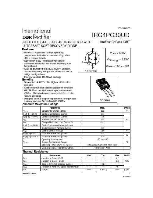
PD 91462B
IRG4PC30UD
INSULATED GATE BIPOLAR TRANSISTOR WITH UltraFast CoPack IGBT
ULTRAFAST SOFT RECOVERY DIODE
Features
C
• UltraFast: Optimized for high operating frequencies 8-40 kHz in hard switching, >200 kHz in resonant mode
Parameter
Min. Typ. Max. Units
Conditions
V(BR)CES Collector-to-Emitter Breakdown VoltageS 600 ∆V(BR)CES/∆TJ Temperature Coeff. of Breakdown Voltage ----
IGBT's . Minimized recovery characteristics require less/no snubbing • Designed to be a "drop-in" replacement for equivalent industry-standard Generation 3 IR IGBT's
Parameter Junction-to-Case - IGBT Junction-to-Case - Diode Case-to-Sink, flat, greased surface Junction-to-Ambient, typical socket mount Weight
Min. -------------------------
29-DSL(CB03)-数字用户板

绿 U5 接口状态指示灯
绿 U6 接口状态指示灯
绿 U7 接口状态指示灯
绿 U8 接口状态指示灯
红 串口通信指示灯
说明
正常状态
同上
亮/灭
同上
亮/灭
同上
亮/灭
同上
亮/灭
同上
亮/灭
同上
亮/灭
同上
亮/灭
1. 闪亮:串口通信正常;
2. 长亮或长灭:单板工作不正 闪 亮 常。
开关及跳线说明
无。
技术指标
1. 性能指标 传输距离:≤4000m(0.4 线径);
6
7
8
DSL
图4 DSL 板外部配线图
6
2
C&C08 数字程控交换系统 单板手册
DSL
3. ET 部分
ET 完成 OSI 开放系统互联参考模型第 1 层和第 2 层功能,包含以下部分:
CPU 部分:微处理器实现 OSI 开放系统互联参考模型第 1 层和第 2 层的软件, 负责处理 D 信道信令和分组数据。
D 信道的插入/提取:可同时进行 8 路 D 信道 HDLC 信令的收发。
串行通信控制器:板内 CPU 通过串行通信控制器与主控制节点交换呼叫处理 信息。
U 接口控制电路:用以实现 CPU 对 D 信道的信令控制,CPU 借助 U 接口控 制电路实现对 U 接口的激活、去激活的控制。
面板及指示灯说明
图 3是 DSL 板面板图,表 1 是 DSL 板指示灯的具体含义。
3
C&C08 数字程控交换系统 单板手册
B 信道交换:“B 信道交换”一方面通过 2 条 2Mbit/s 链路(HW0 和 HW1) 与交换机大网连接,实现 B 信道与 HW 总线之间的交换;另一方面与 V 参考 点(如图 1 所示)的 2Mbit/s 链路相连,提供 B 通道的无阻塞交换功能。
德图400说明书
÷
更换打印纸
纸盒位于打印机的顶部。如图所示装好打印纸。 注:打印纸为热敏打印纸,也就是说只能单面打印。因 此注意正确地安装纸方向 把开关切换到“进行”即可转动纸卷
在接有舒适度探头(0628 0009)的情况下计 算紊流度 该功能键被冻结 在接有 CO 探头情况下,重复校零
- 10 -
Aw 值
NET
温度测量 压力测量 湿度测量 转速测量 风速测量
菜单概览 功能键分配方案
启动测量程序
结束测量程序
在接有温度探头的情况下,利用保存 在 PROBE-T95 fas(t 探头 T95-加速) 中的常数,(也看情况)采用外推法从 读数的变化中得到终值。此功能特别 适于低温探头。常数由电脑软件测得。
参数 温度℃ 湿度%RH 压力 hPa…bar 风速 m/s,m3/h
CO
CO2 转速 电压 V 电流 I WBGT ℃ NET ℃
testo 400 × × × × × × × × × × ×
testo 650 × × × - × × × × × - -
testo 950 × - - - × × × × × - -
德图充电电池
装入电池
打开仪器后盖,把纽扣电池(订货号 0515 0028)装入电池 盒带,“+”符号的一面向上。装入电池或德图充电电池(订 货号 0554 0196)。 注意电池极性!盖上电池盒盖。
参照索引,在“电源”章节进一步了解备选电源、充电模式、 电池质量、充电操作等信息。
纽扣电池-在充电电池耗 尽或更换电池时保存内 存中的数据
Sennheiser evolution wireless G4 SK 300 G4-RC 体包发射

FEATURES• Robust bodypack transmitter for use with any Sennhei-ser headmic or lavalier microphone (HEADMIC 1, ME 2 recommended)• Easy to use, fast setup time• Integrated network port allows control, monitoringand setup via Sennheiser Control Cockpit and WSM Software • Broad range of products and existing accessories (suchas microphones) allows usage in any kind of environ-ment • Up to 88 MHz bandwidth, up to 32 channels • Increased RF output power (10/30/50 mW)• Transmission Range: up to 100 meters / 330 feet • Compatible with wireless speaker system LSP 500 PRO • RC (remote control) switch available for the bodypacktransmitterDELIVERY INCLUDES• SK 300 G4-RC bodypack transmitter • 2 AA batteries • pouch • quick guide • safety guide• manufacturer declaration sheetRobust bodypack transmitter with increased bandwidth and transmission power for evolution wireless G4 300Series systems, delivering exceptional speech intelligibility in Business and Education.ACCESSORIESRMS 1Remote mute switch Art. no. 503164BA 2015rechargeable battery Art. no. 009950L 2015chargerArt. no. 009828CL 2microphone cableArt. no. 004840PRODUCT VARIANTSSK 300 G4-RC-Aw+470 - 558 MHz Art. no. 509541SK 300 G4-RC-AS 520 - 558 MHz Art. no. 509573SK 300 G4-RC-Gw1558 - 608 MHz Art. no. 509548SK 300 G4-RC-Gw 558 - 626 MHz Art. no. 509575SK 300 G4-RC-GBw 606 - 678 MHz Art. no. 509894SK 300 G4-RC-Bw 626 - 698 MHz Art. no. 509530SK 300 G4-RC-Cw 718 - 790 MHz Art. no. 509576SK 300 G4-RC-Dw 790 - 865 MHz Art. no. 509577SK 300 G4-RC-JB 806 - 810 MHzArt. no. 509574SK 300 G4-RC-K+925 - 937.5 MHz Art. no. 509893SPECIFICATIONSRF characteristicsModulation Wideband FM Frequency ranges Aw+: 470 - 558 MHzAS: 520 - 558 MHzGw1: 558 - 608 MHzGw: 558 - 626 MHzGBw: 606 - 678 MHzBw: 526 - 698 MHzCw: 718 - 790 MHzDw: 790 - 865 MHzJB: 806 - 810 MHzK+: 925 - 937.5 MHz Transmission frequencies Max. 3520 frequencies,adjustable in 25 kHz steps20 frequency banks, eachwith up to 32 factory-pre-set channels, no intermo-dulation6 frequency banks withup to 32 programmablechannelsSwitching bandwidth up to 88 MHzNominal/peak deviation±24 kHz / ±48 kHz Frequency stability≤ ±15 ppmRF output power at 50 Ωswitchable:Low: typ. 10 mWStandard: typ. 30 mWHigh: typ. 50 mWPilot tone squelch Can be switched off AF characteristicsCompander system Sennheiser HDXAF frequency response Mic: 80 – 18,000 HzLine: 25 – 18,000 Hz Signal-to-noise ratio (1 mV,peak deviation)≥ 115 dBATotal harmonic distortion(THD)≤ 0.9 %Max. microphone/lineinput voltage3 VeffMicrophone/lineinput impedance40 kΩ, unbalanced / 1 MΩInput capacitance SwitchableSetting range for inputsensitivity60 dB,adjustable in 3 dB steps Overall deviceTemperature range-10 °C to +55 °CPower supply 2 AA batteries, 1.5 V orBA 2015 accupack Nominal voltage 3 V battery /2.4 V rechargeable battery Current consumption at nominal voltage:typ. 180 mAwith transmitter switchedoff: ≤ 25 µAOperating time Typically 8 h Dimensions Approx. 82 x 64 x 24 mm Weight (incl. batteries)approx. 160 gDIMENSIONS3,5mm Klinke 2,5mm KlinkeARCHITECT‘S SPECIFICATIONThe compact bodypack transmitter shall be for use with a companion receiver as part of a wireless RF transmission sys-tem.The bodypack transmitter shall operate within ten UHF frequency ranges, with a switching bandwidth of up to 88 MHz: 470 – 558 MHz, 520 – 558 MHz, 558 – 608 MHz, 558 – 626 MHz, 606 – 678 MHz, 626 – 698 MHz, 718 – 790 MHz, 790 – 865 MHz, 806 – 810 MHz, 925 – 937.5 MHz; transmission frequencies shall be 3520 per range and shall be tunable in 25 kHz steps. The bodypack transmitter shall feature 20 fixed frequency banks with up to 32 compatible frequency presets and 6 user banks with up to 32 user programmable frequencies.The bodypack transmitter shall be menu-driven with a backlit LC display showing the current frequency, frequency bank and channel number, metering of AF level, transmission status, lock status, pilot tone transmission, muting function, and battery status. An auto-lock feature shall be provided to prevent settings from being accidentally altered.The bodypack transmitter parameters shall either be configurable in the associated receiver’s menu and synchronized with the bodypack transmitter via an integrated infrared interface or shall be programmable in the bodypack transmitter menu.The bodypack transmitter shall be equipped with a mute switch, which shall be switchable between “AF on/off”, “RF on/ off” and “Disabled” via the receiver’s user interface. A 2.5 mm jack socket shall be provided for connecting a Sennheiser RMS 1 external mute switch. The settings for the external mute switch shall be switchable between “AF on/off”, “RF on/ off”, “Push to mute” and “Push to talk” via the user interface.Nominal/peak deviation shall be ±24 kHz/±48 kHz. Frequency stability shall be ≤ ±15 ppm. RF output power at 50 Ω shall be switchable between 10 mW (typical, low) and 30 mW (typical, standard) and 50 mW (typical, high).The bodypack transmitter shall incorporate the Sennheiser HDX compander system and a defeatable pilot tone squelch. Audio frequency response shall range from 80 – 18,000 Hz (microphone) or 25 - 18,000 Hz (line). Signal-to-noise ratio at 1 mV and peak deviation shall be ≥ 115 dBA. Total harmonic distortion (THD) shall be ≤ 0.9 %. Input sensitivity shall be adjustable within a 60 dB range in steps of 3 dB.Power shall be supplied to the bodypack transmitter by two 1.5V AA size batteries or by one Sennheiser BA 2015 rechar-geable accupack. Nominal voltage shall be 2.4 V, current consumption shall be typical 180 mA at nominal voltage; ≤ 25 µA when bodypack transmitter is switched off. Operating time shall be typical 8 hours. The bodypack transmitter shall have a rugged metal housing; dimensions shall be approximately 82 x 64 x 24 mm (3.23" x 2.52" x 0.94"). Weight including the batteries shall be approximately 160 grams (5.64 oz). Operating temperature shall range from −10 °C to +55 °C (+14 °F to +131 °F).The bodypack transmitter shall be the Sennheiser SK 300 G4-RC.Sennheiser electronic GmbH & Co. KG · Am Labor 1 · 30900 Wedemark · Germany · 。
B404中文资料

VOLTAGE RANGE 200 to 400 Volts B302 THRU B304CURRENT40.0 AmperesTECHNICAL SPECIFICATION : FEATURES• Low Leakage• Low forward voltage drop • High current capability• High forward surge current capacity •Glass passivated chipMECHANICAL DATA• Technology: vacuum soldered• Copper cup with transfer molded plastic • Polarity: B30-P lead-PB30-N lead-N• Lead: Plated Ni lead, solderable per MIL-STD-202E method 208C • Mounting: Press Fit•Weight: 0.094 ounces, 2.65 gramsMAXIMUM RATINGS AND ELECTRICAL CHARACTERISTICS• Ratings at 25℃ ambient temperature unless otherwise specified • Single Phase, half wave, 60HZ, resistive or inductive load •For capacitive load derate current by 20%SYMBOLS B402-P B402-N B403-P B403-N B404-P B404-N UNIT Maximum Repetitive Peak Reverse Voltage V RRM 200 300 400 Volts Maximum RMS Voltage V RMS 140 210 280 Volts Maximum DC Blocking VoltageV DC 200300 400Volts Maximum Average Forward Rectified Current, At Tc=105℃I O40AmpsPeak Forward Surge Current3.3mS single half sine wave superimposed on Rated load (JEDEC method) I FSM 500 Amps Rating for fusing (t <8.3ms)I 2t 1037 A 2S Maximum instantaneous Forward Voltage at 100A V F 1.10 Volts 5.0 Maximum DC Reverse Current at Rated TA=25℃ DC Blocking Voltage TA=100℃ I R 450 UA Typical Thermal ResistanceR θJC 1.0 ℃/W Operating and Storage Temperature RangeT J ,T STG(-65 to +175)℃Notes:1. Enough heatsink must be considered in application.VOLTAGE RANGE 200 to 400 Volts B402 THRU B404CURRENT40.0 AmperesRATINGS AND CHARACTERISTIC CURVES B402 THRU B404F1G.2 MAXIMUM NON-REPETITIVE PEAKFORWARD SURGE CURRENTF1G.1 TYPICAL FORWARD CURRENTDERATING GURVENUMBER OF CYCLES AT 60 Hz1006040201086421P E A K F O R W A R D S U R G E C UR R E N T ,(A )A V E R A G E F O R W A R D C U R R E N T ,(A )AMBIENT TEMPERATURE, ()℃125100150175755025020********F1G.3 TYPICAL INSTANTANEOUS FORWARD CHARACTERISTICSI N S T A N T A N E O U S F O R W A R D C U R R E N T ,(A )INSTANTANEOUS FORWARD VOLTAGE,(V)1000101.00.1504030200604020A V E R A G E P O W E R D I S S I P A T I O N (W )AVERAGE FORWARD CURRENT, (A)F1G.4 FORWARD ROWER DISSIPATION1050。
三汇示波器说明书(Ver1.0)
DST4000 和 DST1000 系列数字存储示波器用户手册
i
目录
5.1 显示区 ........................................................................................ 20 5.2 信息区域..................................................................................... 23 5.3 波形显示..................................................................................... 23
三汇系列产品
DST4000 和 DST1000 系列 数字存储示波器
Version 1.0
杭州三汇科技有限公司 www.
目录
目录
目 录 ...........................................................................................................i 版权申明 .......................................................................................................................................................................v 第 1 章 安全事项......................................................................................... 1
IRG4BC20UD中文资料

A
1
10
100
f, Frequency (kHz)
Fig. 1 - Typical Load Current vs. Frequency (Load Current = IRMS of fundamental)
IC , Collector-to-Emitter Current (A)
100
TJ = 25°C TJ = 150°C
Absolute Maximum Ratings
TO-220AB
VCES IC @ TC = 25°C IC @ TC = 100°C ICM ILM IF @ TC = 100°C IFM VGE PD @ TC = 25°C PD @ TC = 100°C TJ TSTG
Parameter Collector-to-Emitter Voltage Continuous Collector Current Continuous Collector Current Pulsed Collector Current Q Clamped Inductive Load Current R Diode Continuous Forward Current Diode Maximum Forward Current Gate-to-Emitter Voltage Maximum Power Dissipation Maximum Power Dissipation Operating Junction and Storage Temperature Range Soldering Temperature, for 10 sec. Mounting Torque, 6-32 or M3 Screw.
Parameter Junction-to-Case - IGBT Junction-to-Case - Diode Case-to-Sink, flat, greased surface Junction-to-Ambient, typical socket mount Weight
- 1、下载文档前请自行甄别文档内容的完整性,平台不提供额外的编辑、内容补充、找答案等附加服务。
- 2、"仅部分预览"的文档,不可在线预览部分如存在完整性等问题,可反馈申请退款(可完整预览的文档不适用该条件!)。
- 3、如文档侵犯您的权益,请联系客服反馈,我们会尽快为您处理(人工客服工作时间:9:00-18:30)。
Forward Transconductance T
3.1
ICES
Zero Gate Voltage Collector Current
----
----
VFM
Diode Forward Voltage Drop
----
----
IGES
Gate-to-Emitter Leakage Current
----
Fig. 1 - Typical Load Current vs. Frequency (Load Current = IRMS of fundamental)
IC , Collector-to-E mitter Current (A)
100
TJ = 25°C TJ = 150°C
10
1
0.1 0.1
G
E
n-channel
VCES = 600V VCE(on) typ. = 1.95V @VGE = 15V, IC = 12A
TO-220AB
Absolute Maximum Ratings
VCES IC @ TC = 25°C IC @ TC = 100°C ICM ILM IF @ TC = 100°C IFM VGE PD @ TC = 25°C PD @ TC = 100°C TJ TSTG
Parameter
Min. Typ. Max. Units
Conditions
V(BR)CES Collector-to-Emitter Breakdown VoltageS 600 ∆V(BR)CES/∆TJ Temperature Coeff. of Breakdown Voltage ----
Parameter Collector-to-Emitter Voltage Continuous Collector Current Continuous Collector Current Pulsed Collector Current Q Clamped Inductive Load Current R Diode Continuous Forward Current Diode Maximum Forward Current Gate-to-Emitter Voltage Maximum Power Dissipation Maximum Power Dissipation Operating Junction and Storage Temperature Range Soldering Temperature, for 10 sec. Mounting Torque, 6-32 or M3 Screw.
See Fig. 9, 10, 11, 18
TJ = 150°C, See Fig. 9, 10, 11, 18 IC = 12A, VCC = 480V VGE = 15V, RG = 23Ω Energy losses include "tail" and
diode reverse recovery.
• Generation 4 IGBT design provides tighter parameter distribution and higher efficiency than Generation 3
• IGBT co-packaged with HEXFREDTM ultrafast, ultra-soft-recovery anti-parallel diodes for use in bridge configurations
VGE = 0V, IC = 1.0mA
IC = 12A
VGE = 15V
IC = 23A
See Fig. 2, 5
IC = 12A, TJ = 150°C
VCE = VGE, IC = 250µA
VCE = VGE, IC = 250µA
VCE = 100V, IC = 12A
VGE = 0V, VCE = 600V
Max. 600 23 12 92 92 12 92 ± 20 100 42 -55 to +150
300 (0.063 in. (1.6mm) from case) 10 lbf•in (1.1 N•m)
Units V
A
V W °C
Thermal Resistance
RθJC RθJC RθCS RθJA Wt
---- ---- V 0.63 ---- V/°C 1.95 2.1 2.52 ---- V 2.09 ------- 6.0 -11 ---- mV/°C 8.6 ---- S ---- 250 µA ---- 2500 1.4 1.7 V 1.3 1.6 ---- ±100 nA
VGE = 0V, IC = 250µA
Conditions
IC = 12A VCC = 400V
See Fig. 8
VGE = 15V TJ = 25°C
IC = 12A, VCC = 480V VGE = 15V, RG = 23Ω
Energy losses include "tail" and
diode reverse recovery.
Min. -------------------------
Typ. ----------0.50 ----2 (0.07)
Max. 1.2 2.5 -----80 ------
Units °C/W
g (oz)
1
4/17/00
元器件交易网
IRG4BC30UD
Electrical Characteristics @ TJ = 25°C (unless otherwise specified)
VR = 200V
TJ = 125°C
16 di/dt 200A/µs
TJ = 25°C See Fig.
TJ = 125°C 17
2
元器件交易网
Load Current ( A )
16
12
60% of rated
8
vo ltage
I
4
0 0.1
IRG4BC30UD
Parameter Junction-to-Case - IGBT Junction-to-Case - Diode Case-to-Sink, flat, greased surface Junction-to-Ambient, typical socket mount Weight
Diode Peak Reverse Recovery Current
Diode Reverse Recovery Charge
Diode Peak Rate of Fall of Recovery During tb
Min. Typ. Max. Units ---- 50 75 ---- 8.1 12 nC ---- 18 27 ---- 40 ------- 21 ---- ns ---- 91 140 ---- 80 130 ---- 0.38 ------- 0.16 ---- mJ ---- 0.54 0.9 ---- 40 ------- 22 ---- ns ---- 120 ------- 180 ------- 0.89 ---- mJ ---- 7.5 ---- nH ---- 1100 ------- 73 ---- pF ---- 14 ------- 42 60 ns ---- 80 120 ---- 3.5 6.0 A ---- 5.6 10 ---- 80 180 nC ---- 220 600 ---- 180 ---- A/µs ---- 120 ----
IGBTs . Minimized recovery characteristics require less/no snubbing
• Designed to be a "drop-in" replacement for equivalent industry-standard Generation 3 IR IGBTs
• Industry standard TO-220AB package
Benefits
• Generation -4 IGBT's offer highest efficiencies available
• IGBTs optimized for specific application conditions • HEXFRED diodes optimized for performance with
VCE(on)
Collector-to-Emitter Saturation Voltage -------
----
VGE(th)
Gate Threshold Voltage
3.0
∆VGE(th)/∆TJ Temperature Coeff. of Threshold Voltage ----
gfe
VGE = 15V 20µs PU LSE W ID TH A
1
10
VCE , C o lle ctor-to -Em itter Vo ltag e (V)
Fig. 2 - Typical Output Characteristics
Measured 5mm from package
VGE = 0V VCC = 30V
See Fig. 7
ƒ = 1.0MHz
TJ = 25°C See Fig.
TJ = 125°C 14 TJ = 25°C See Fig.
IF = 12A
TJ = 125°C 15 TJ = 25°C See Fig.