810-002-SP2L001;中文规格书,Datasheet资料
L-USS810M-DT资料

Data Sheet, Rev. 6March 2006USS810 USB 2.0Full-Speed/Low-Speed Transceiver1 FeaturesComplies with Universal Serial Bus Specification Rev. 2.0.Can be used as a USB device transceiver or a USB host transceiver.Supports full-speed (12 Mbits/s) and low-speed (1.5 Mbits/s) serial data rates.Includes two single-ended receivers with hystere-sis.Low-power operation helps maximize battery life of portable electronic devices.Available in a small MLCC16 package measuring 3mm x 3mm. (A lead-free package is also avail-able. See Ordering Information on page14.)Supports a digital I/O voltage range from 1.75 V to 3.3 V.Supports the full industrial operating temperature range, −40°C to +85 °C.2 DescriptionAgere’s USS810 is a Universal Serial Bus (USB) transceiver that is fully compliant with the Universal Serial Bus Specification Rev. 2.0. The USS810 can transmit and receive serial data at full-speed(12Mbits/s) and low-speed (1.5 Mbits/s) data rates and, therefore, can be used as either a USB device transceiver or a USB host transceiver.Since the USS810 operates at digital I/O voltages between 1.75 V to 3.3 V, it is particularly suitable for portable electronic devices such as mobile phones, digital still cameras, personal digital assistants (PDAs), and a variety of information appliances. This transceiver provides an ideal interface to the physical layer of the universal serial bus for application-spe-cific ICs (ASICs) and programmable logic devices (PLDs) with power supply voltages in the above range.The USB transceiver is currently available in an MLCC16 package that supports single-ended input data interface.3 Suitable ApplicationsPortable electronic devices, such as the following:Mobile phoneDigital still cameraPersonal digital assistant (PDA)Information appliancesUSS810 USB 2.0Data Sheet, Rev. 6 Full-Speed/Low-Speed Transceiver March 2006Table of ContentsContents Page1 Features (1)2 Description (1)3 Suitable Applications (1)4 Functional Diagram (3)5 Pin Information (3)5.1 Pin Descriptions (4)6 Functional Description (5)6.1 Function Selection (5)6.1 Operating Functions (5)7 Limiting Values (6)7.1 Absolute Maximum Ratings (6)8 Static Characteristics (6)9 Dynamic Characteristics (8)10 Test Information (11)11 Package Outline Diagrams (12)11.1 16-Pin MLCC, 3 mm x 3 mm (12)12 USB Application Support Contact Information (14)13 Ordering Information (14)Figure PageFigure 1. USS810 Functional Diagram (3)Figure 2. USS810 MLCC Pin Diagram (Top View) (3)Figure 3. Rise and Fall Times (9)Figure 4. Timing of OE to D+, D– (10)Figure 5. Timing of D+, D– to RCV, VP, VM (10)Figure 6. Timing of VO, FSE0 to D+, D– (10)Figure 7. Load for D+, D– (11)Table PageTable 1. USS810 Pin Description (4)Table 2. Function Table (5)Table 3. Transmit Function Using Single-Ended Input Data Interface (OE = L) (5)Table 4. Receive Function (OE = H) (5)Table 5. Absolute Maximum Ratings (6)Table 6. Recommended Operating Conditions (6)Table 7. Static Characteristics: Supply Pins (6)Table 8. Static Characteristics: Digital Pins (7)Table 9. Static Characteristics: Analog I/O Pins (D+, D–) (7)Table 10. Dynamic Characteristics: Analog I/O Pins (D+, D–)1 (8)Table 11. Pitch Variation (13)Table 12. Common Dimensions (13)2Agere Systems Inc.Agere Systems Inc.3Data Sheet, Rev. 6USS810 USB 2.0March 2006Full-Speed/Low-Speed Transceiver4 Functional Diagram1. Connect pull-up to D– for low-speed operation.Figure 1. USS810 Functional Diagram5 Pin InformationFigure 2. USS810 MLCC Pin Diagram (Top View)LEVEL SHIFTERGNDVMVPRCVSUSPNDOE VO V DD(I/O)SOFTCONSPEED FSE0+–D–D+24 Ω (1%)24 Ω (1%)1.5 k Ω1V PU(3.3)V DD12111098765131415161234RCV USS810MLCCOE SOFTCON V PU(3.3)NU V DD VP VMFSE0VO D+D–SPEEDV DD(I/O)GNDSUSPND4Agere Systems Inc.USS810 USB 2.0Data Sheet, Rev. 6Full-Speed/Low-Speed Transceiver March 20065 Pin Information (continued)5.1 Pin DescriptionsTable 1. USS810 Pin Description 1. Symbol names with an overscore (e.g., NAME) indicate active-low signals.Symbol MLCC Pin Type DescriptionV PU(3.3)15—Pull-Up Voltage Source. Connect this pin through an external 1.5 k Ω resistor to D+ (for full-speed operation) or D– (for low-speed operation). This pin’s function is controlled by the SOFTCON input pin. T o ensure zero pull-up current, set SOFTCON =low to cause V PU(3.3) to float (high impedance); when SOFTCON =high, V PU(3.3) = 3.3 V .SOFTCON 16ISoftware-Controlled USB Connection. This pin allows USB connect/disconnect signaling to be controlled by software. A high level on this pin applies 3.3 V to pin V PU(3.3), which is connected to an external 1.5 k Ω pull-up resistor.OE 11I Output Enable. This active-low pin enables the transceiver to transmit data on the USB bus.RCV 2O Differential Data Receiver. When the SUSPND input is high, this pin is driven low. The state of RCV is unknown when FSE0 = 1.VP 3O Single-Ended D+ Receiver. The VP pin is used for external detection of single-ended zero (SE0), error conditions, and speed of connected device.VM 4O Single-Ended D − Receiver. The VM pin is used for external detection of single-ended zero (SE0), error conditions, and speed of connected device.SUSPND5ISuspend. When SUSPND is high, it enables a low-power state while the USB is inactive and drives output RCV to a low level. No dc power is consumed when SUSPND is high.GND 6P Device Ground.V DD(I/O)7P Power Supply for Digital I/O. 1.75 V to 3.3 V.SPEED8ISpeed Selection. This pin adjusts the slew rate of differential data outputs D+ and D–. Tie this pin low to enable low-speed data transmission (1.5 Mbits/s) and high to enable full-speed data transmission (12 Mbits/s).D–9Analog I/O Negative USB Differential Data Bus. If this device is used in a USB peripheral application, connect an external 24 Ω ± 1% resistor in series with this signal inorder to meet the USB Specification , Rev. 2.0 impedance requirement. Connect this signal to pin V PU(3.3) via a 1.5 k Ω ± 5% resistor for low-speed USB peripheral applications.D+10Analog I/O Positive USB Differential Data Bus. If this device is used in a USB peripheral application, connect an external 24 Ω ± 1% resistor in series with this signal inorder to meet the USB Specification Rev. 2.0 impedance requirement. Connect thissignal to pin V PU(3.3) via a 1.5 k Ω ± 5% resistor for full-speed USB peripheral appli-cations.VO 11I Single-Ended Data Input. Refer to T able 3..FSE012I Single-Ended Zero Mode. Refer to T able 3..V DD 13P 3.3 V Power Supply. This voltage supply is used for the USB signals D+/D– and the internal level shifter.NU14—Not Usable. No external connections to this pin are allowed.Agere Systems Inc.5Data Sheet, Rev. 6USS810 USB 2.0March 2006Full-Speed/Low-Speed Transceiver6 Functional Description6.1 Function SelectionTable 2. Function Table 1. Signal levels on (D +, D–) are determined by other USB devices and external pull-up/down resistors.2. In suspend mode (SUSPND = high), the differential receiver is inactive and output RCV is always low. Out-of-suspend (K) signaling is detected via the single-ended receivers VP and VM.3. In suspend mode, the D+/D– output is tristated.6.1 Operating FunctionsTable 3. Transmit Function Using Single-Ended Input Data Interface (OE = L)1. The state of RCV is unknown when FSE0 = 1.SUSPNDOE (D+, D–)RCV VP/VM FunctionL L Transmitting and Receiving Active Active Normal transmit (differential receiver active)L H Receiving 1Active Active ReceivingH L High-Z 3L 2Active T ransmitting during suspend (differential receiver inactive)HHHigh-Z 3L 2ActiveLow-power stateFSE0VO DataL L Differential logic 0L H Differential logic 1H L SE0HHSE0(D+, D–)RCV VP VM Differential Logic 0L L H Differential Logic 1H H L SE0Unknown 1LL6Agere Systems Inc.USS810 USB 2.0Data Sheet, Rev. 6Full-Speed/Low-Speed Transceiver March 20067 Limiting Values7.1 Absolute Maximum RatingsStresses in excess of the absolute maximum ratings can cause permanent damage to the device. These are abso-lute stress ratings only. Functional operation of the device is not implied at these or any other conditions in excess of those given in the operational sections of the data sheet. Exposure to absolute maximum ratings for extended periods can adversely affect device reliability.Table 5. Absolute Maximum RatingsTable 6. Recommended Operating Conditions 8 Static CharacteristicsTable 7. Static Characteristics: Supply PinsV DD = 3.3 V; V DD(I/O) = 1.75 V to 3.3 V; V GND = 0 V; T amb = –40 °C to +85 °C; unless otherwise specified.Symbol Parameter ConditionsMin Max Unit V DD(I/O)I/O Supply Voltage — 1.7 3.3V V DD(3.3)3.3 V Supply Voltage — 3.0 3.6V V I dc Input Voltage—–0.5V DD + 0.5V T stgStorage T emperature—–40125°CSymbol ParameterConditionsMin Typical Max Unit V DD(I/O)I/O Supply Voltage — 1.75— 3.3V V DD(3.3)3.3 V Supply Voltage 3.3 V operation 3.135 3.3 3.465V V I Input Voltage —0— 3.3V V I(AI/O)Input Voltage on Analog I/O Pins (D+/D–)—0—V DD(I/O)V T ambOperating Ambient Temperature—–40—85°CSymbol ParameterConditions Min Typical Max Unit I DD Operating Supply Current Full-speed transmit andreceive —58mA I DD(I/O)Operating I/O Supply CurrentFull-speed transmit and receive at 12 Mbits/s ——100µA I DD(susp)Suspend Supply CurrentSUSPND = high——10µAAgere Systems Inc.7Data Sheet, Rev. 6USS810 USB 2.0March 2006Full-Speed/Low-Speed Transceiver8 Static Characteristics (continued)Table 8. Static Characteristics: Digital PinsV DD(I/O) = 1.75 V to 3.3 V; V GND = 0 V; T amb = −40 °C to +85 °C; unless otherwise specified.Table 9. Static Characteristics: Analog I/O Pins (D+, D–)V DD = 3.3 V; V GND = 0 V; T amb = −40 °C to +85 °C; unless otherwise specified.SymbolParameterConditionsMinTypicalMaxUnitV DD(I/O) = 1.75 V to 3.3 VInput Levels:V IL Low-level Input Voltage———0.7V V IHHigh-level Input Voltage — 1.7——V Output Levels:V OL Low-level Output VoltageI OL ≤ 6 mA ——0.4V V OHHigh-level Output Voltage I OH ≤ 6 mAV DD – 0.4——VSymbol Parameter Conditions Min Typical Max UnitInput LevelsDifferential ReceiverV DI Differential Input Sensitivity IV I(D+) – V I(D–)I 0.2——V V CMDifferential Common-mode VoltageIncludes V DI range 0—V DD VSingle-Ended ReceiverV hysHysteresis Voltage —0.3——V Output LevelsV OL Low-level Output VoltageR L = 1.5 k Ω to3.6V——0.3V V OH High-level Output Voltage R L = 15 k Ω to GND2.8—3.6V Leakage CurrentI LZ High-impedance LeakageCurrentOE = 1–10—10µACapacitanceC IN T ransceiver CapacitancePin to GND ——3pF8Agere Systems Inc.USS810 USB 2.0Data Sheet, Rev. 6Full-Speed/Low-Speed Transceiver March 20069 Dynamic CharacteristicsTable 10. Dynamic Characteristics: Analog I/O Pins (D+, D–)1V DD = 3.3 V; V DD(I/O) = 1.75 V to 3.3 V; V GND = 0 V; Tamb = –40°C to +85°C; unless otherwise specified.1. T est circuit: see Figure 7.SymbolParameterConditionsMin Typical Max UnitDriver CharacteristicsFull-Speed Mode (Speed = 1)t RRise TimeOE = 0, CL = 50 pF;10% to 90% of |V OL − V OH |;see Figure 3..4—20nst F Fall Time OE = 0, CL = 50 pF;90% to 10% of |V OH − V OL |;see Figure 3.4—20nsDRFM Differential Rise/Fall Time Matching OE = 0, CL = 50 pF .90100110%V CRSOutput Signal Crossover VoltageOE = 0, CL = 50 pF:see Figures 4, 5, 6. 1.3—2.0VLow-Speed Mode (Speed = 0)t RRise Time OE = 0, CL = 50 pF or 350pF; 10% to 90% of |V OL − V OH |;see Figure 3.75—300nst F Fall Time OE = 0, CL = 50 pF or 350pF; 90% to 10% of |V OH − V OL |;see Figure 3.75—300nsDRFM Differential Rise/Fall Time Matching CL = 50 pF or 350pF .80100120%V CRSOutput Signal Crossover VoltageCL = 50 pF or 350pF;see Figures 4, 5, 6. 1.3—2.0VDriver TimingFull-Speed Mode (Speed = 1)t PLH Driver Propagation Delay:Low-to-High (VO, FSE0 to D+, D–)OE = 0, CL = 50 pF; see Figure 6.——18ns t PHL Driver Propagation Delay:High-to-Low (VO, FSE0 to D+, D–)OE = 0, CL = 50 pF; see Figure 6.——18ns t PHZ Tristate Output Disable: High-to-Off (OE to D +, D −)OE switching; see Figure 4.—— 2.5ns t PLZ Tristate Output Disable: Low-to-Off (OE to D +, D −)OE switching; see Figure 4.—— 2.5ns t PZH Tristate Output Enable: Off-to-High (OE to D +, D −)OE switching; see Figure 4.——20ns t PZLTristate Output Enable: Off-to-Low (OE to D +, D −)OE switching; see Figure 4.——20nsData Sheet, Rev. 6USS810 USB 2.0 March 2006Full-Speed/Low-Speed Transceiver10Agere Systems Inc.Agere Systems Inc.11Data Sheet, Rev. 6USS810 USB 2.0March 2006Full-Speed/Low-Speed Transceiver10 Test InformationLoad Capacitance:CL = 50 pF (full-speed mode).CL = 50 pF or 350 pF (low-speed mode).1. Full-speed mode: connected to D+, low-speed mode: connected to D–.2. Complies with USB2.0.Figure 7. Load for D+, D–24 Ω2DUTV PU(3.3)15 k ΩD+/D–TEST POINTC L1.5 k Ω1USS810 USB 2.0Data Sheet, Rev. 6 Full-Speed/Low-Speed Transceiver March 200611 Package Outline Diagram11.1 16-Pin MLCC, 3 mm x 3 mmDimensions are in millimeters.1. Die thickness allowable is 0.305 mm maximum (0.012 inches maximum).2. Dimensioning and tolerances conform to ASME Y14.5M-1994.3. N is the number of terminals. Nd is the number of terminals in X direction, and Ne is the number of terminals in the Y direction.4. Dimension b applies to plated terminal and is measured between 0.2 mm and 0.25 mm from terminal tip.5. The pin #1 identifier must be existed on the top surface of the package by using identification mark or other feature of package body.6. Exact shape and size of this feature is optional.7. All dimensions are in millimeters.8. The shape shown on four corners is not actual I/O.9. Bilateral coplanarity zone applies to the exposed pad as well as the terminals.10. Applied only for terminals.11. Q and R apply only for straight tie bar shapes.12Agere Systems Inc.Agere Systems Inc.13Data Sheet, Rev. 6USS810 USB 2.0March 2006Full-Speed/Low-Speed Transceiver11 Package Outline Diagram (continued)Table 11. Pitch Variation Table 12. Common DimensionsSymbolPitch VariationNotesMinNom Maxe 0.5 BSC —N 163Nd 43Ne 43L 0.30.40.5—b 0.180.230.34D2 1.40 1.50 1.60—E21.40 1.501.60—SymbolCommon DimensionsNotesMinNom Max A 0.80.850.9—A10.00.010.0511A20.60.650.70—A30.20 REF —D 3.0 BSC —D1 2.75 BSC —E 3.0 BSC —E1 2.75 BSC—θ0—12—P 0.240.420.6—R0.130.170.2312USS810 USB 2.0Data Sheet, Rev. 6Full-Speed/Low-Speed Transceiver March 2006Agere Systems Inc. reserves the right to make changes to the product(s) or information contained herein without notice. No liability is assumed as a result of their use or application. Agere, Agere Systems, and the Agere logo are registered trademarks of Agere Systems Inc.Copyright © 2006 Agere Systems Inc.All Rights ReservedMarch 2006DS05-035CMPR-6 (Replaces DS05-035CMPR-5)For additional information, contact your Agere Systems Account Manager or the following:INTERNET:Home: Sales: /sales E-MAIL:docmaster@N. AMERICA:Agere Systems Inc., Lehigh Valley Central Campus, Room 10A-301C, 1110 American Parkway NE, Allentown, PA 18109-91381-800-372-2447, FAX 610-712-4106 (In CANADA: 1-800-553-2448, FAX 610-712-4106)ASIA:CHINA: (86) 21-54614688 (Shanghai), (86) 755-25881122 (Shenzhen), (86) 10-65391096 (Beijing)JAPAN: (81) 3-5421-1600 (Tokyo), KOREA: (82) 2-767-1850 (Seoul), SINGAPORE: (65) 6741-9855, TAIWAN: (886) 2-2725-5858 (Taipei)EUROPE:Tel. (44) 1344 296 40012 USB Application Support Contact InformationE-mail: usb@13 Ordering Information*Lead-free: No intentional addition of lead, and less than 1000 ppm.†Agere Systems lead-free devices are fully compliant with the Restriction of Hazardous Substances (RoHS) directive that restricts the content of six hazardous substances in electronic equipment in the European Union. Beginning July 1, 2006, electronic equipment sold in the Euro-pean Union must be manufactured in accordance with the standards set by the RoHS directive.Device Code DescriptionPackage Comcode USS810M-D USS810 in dry-packed tubeMLCC16700057479USS810M-DT USS810 in dry-packed tape and reel MLCC16700058082L-USS810M-D*†Lead-free USS810 in dry-packed tubeMLCC16700067200L-USS810M-D*†Lead-free USS810 in dry-packed tape and reelMLCC16700067201。
技术规格仕样书810P

序号 1 2 3 项 行宽 分辨率 打印方式 汉字 汉字(高速打印) 汉字(超高速打印) 英数字 英数字(高速) 英数字(高速低质) 目 DPK810P打印机(106列) 106列 180DPI 24针点阵式 78KPS 156KPS 225 KPS 156CPS 312CPS 468CPS 0.2 毫米 1/180英寸 1/180英寸 90字符/行 181字符/行 24×24点 24×12点 19×13点 双向(自动判断最短距离进行正反向打印) 2MM 45~340mm 76~330mm 1+7份 1+7份 1908点/行 180点/英寸 180点/英寸 摩擦走纸 推进式链式走纸 1/120英寸× n 5.6IPS 85毫秒 运行时:5~35℃ 非运行时:-15~60℃ (温度升降为15℃/H以下) 运行时:20~80%RH 非运行时:5~95%RH (不结露,湿度升降为30%RH/日以下, 最高湿球温度29℃以下) IEEE-1284双向并行接口 RS232串口(选件) USB接口(选件) 市电单向 198~264伏 50~60Hz+2%,-4% <15W <5分钟 <1W 240W 519mm 292mm 202mm 12Kg <55dBA ≥12000小时 0.3H 5年 4亿次/针 有接头扭带盒方式(25m) >1000万字(英数字) 自动 手动 有(选件) 无 有 断针自动补偿 仿真自动匹配 超宽自动无级变倍压缩 计算机端打印机参数设置 在线自动更新 大字库 GB18030 GB4943 名称: DPK810P技术规格书 图号: 备 注
4
ቤተ መጻሕፍቲ ባይዱ
打印速度
5 6 7
8 9 10 11 12
13
10-810-90C;14-810-90C;16-810-90C;08-6810-90C;10-2810-90C;中文规格书,Datasheet资料

All tolerances ± .005 [.13] unless otherwise specified
Consult factory for non-standard sizes.
Note: Aries specializes in custom design and production. In addition to the standard products shown on this page, special materials, platings, sizes, and configurations can be furnished, depending on quantities. Aries reserves the right to change product specifications without notice.
Dim. “Z” .300 [7.62] .400 [10.16] .500 [12.70] .700 [17.78]
Available Sizes 8, 10
8, 10, 12, 14, 16 8, 10
8, 10, 12, 14, 16
“W”=NO. OF PINS PER ROW X .100 [2.54] “X”=(NO. OF PINS PER ROW - 1) X .100 [2.54]
Series 800 Vertisockets™ Vertical Mounting with Collet Contacts
FEATURES: • Aries offers a full line of VertisocketsTM for DIP packaging of
RUE002N02TL;中文规格书,Datasheet资料

10000 VGS= 4.0V Pulsed
1000
Ta=125°C Ta=75°C Ta=25°C Ta= -25°C
10000 VGS= 2.5V Pulsed
1000
Ta=125°C Ta=75°C Ta=25°C Ta= -25°C
100
0.001
0.01
0.1
1
DRAIN-CURRENT : ID[A]
STATIC DRAIN-SOURCE ON-STATE RESISTANCE : RDS(on)[mΩ]
STATIC DRAIN-SOURCE ON-STATE RESISTANCE : RDS(on)[mΩ]
10000 Ta= 25°C Pulsed
1000
VGS= 1.2V VGS= 1.5V VGS= 1.8V VGS= 2.5V VGS= 4.0V
100
0.001
0.01
0.1
1
DRAIN-CURRENT : ID[A]
Fig.6 Static Drain-Source On-State Resistance vs. Drain Current(Ⅱ)
STATIC DRAIN-SOURCE ON-STATE RESISTANCE : RDS(on)[mΩ]
Input capacitance
Ciss
−
Output capacitance
Coss
−
Reverse transfer capacitance Turn-on delay time Rise time
Crss
−
td(on) ∗
−
tr ∗ −
Turn-off delay time Fall time
3590S-2-502L;3590S-2-102L;3590S-2-103L;3590S-2-203L;3590S-1-502L;中文规格书,Datasheet资料

Specifi cations are subject to change without notice.Customers should verify actual device performance in their specifi c applications.*RoHS Directive 2002/95/EC Jan. 27, 2003 including annex and RoHS Recast 2011/65/EU June 8, 2011.Stop Strength..............................................................................................................................................................................45 N-cm (64 oz.-in.) minimum Mechanical Angle ...........................................................................................................................................................................................3600 ° +10 °, -0 °Torque (Starting & Running) ................................................................................................................................0.35 N-cm (0.5 oz.-in.) maximum (unsealed) 1.1 N-cm (1.5 oz.-in.) maximum (sealed) Mounting ..............................................................................................................................................................................55-80 N-cm (5-7 lb.-in.) (plastic) 90-113 N-cm (8-10 in.-lb.) (metal)Shaft Runout......................................................................................................................................................................................0.13 mm (0.005 in.) teral Runout ...................................................................................................................................................................................0.20 mm (0.008 in.) T.I.R.Shaft End Play ...................................................................................................................................................................................0.25 mm (0.010 in.) T.I.R.Shaft Radial Play ...............................................................................................................................................................................0.13 mm (0.005 in.) T.I.R.Pilot Diameter Runout .......................................................................................................................................................................0.08 mm (0.003 in.) T.I.R.Backlash ............................................................................................................................................................................................................1.0 ° maximum Weight ........................................................................................................................................................................................................Approximately 19 G Terminals ................................................................................................................................................................................................Solder lugs or PC pins Soldering ConditionManual Soldering...........................................................96.5Sn/3.0Ag/0.5Cu solid wire or no-clean rosin cored wire; 370 °C (700 °F) max. for 3 seconds Wave Soldering ...................................................................................96.5Sn/3.0Ag/0.5Cu solder with no-clean fl ux; 260 °C (500 °F) max. for 5 seconds Wash processes .......................................................................................................................................................................................Not recommended Marking .....................................Manufacturer’s name and part number, resistance value and tolerance, linearity tolerance, wiring diagram, and date code.Ganging (Multiple Section Potentiometers) ......................................................................................................................................................1 cup maximum Hardware ............................................................................................................One lockwasher and one mounting nut is shipped with each potentiometer.NOTE: For Anti-rotation pin add 91 after confi guration dash number. Example: -2 becomes -291 to add AR pin.1At room ambient: +25 °C nominal and 50 % relative humidity nominal, except as noted. 2Consult manufacturer for complete specifi cation details for resistances below 1k ohms.BOLDFACE LISTINGS ARE IN STOCK AND READILY AVAILABLETHROUGH DISTRIBUTION. FOR OTHER OPTIONS CONSULT FACTORY.ROHS IDENTIFIER: L = COMPLIANTRecommended Part Numbers(Printed Circuit)(Solder Lug)(Solder Lug)Resistance (Ω)Resolution (%)3590P-2-102L 3590S-2-102L 3590S-1-102L 1,000.0293590P-2-202L 3590S-2-202L 3590S-1-202L 2,000.0233590P-2-502L 3590S-2-502L 3590S-1-502L 5,000.0253590P-2-103L 3590S-2-103L 3590S-1-103L 10,000.0203590P-2-203L 3590S-2-203L 3590S-1-203L 20,000.0193590P-2-503L 3590S-2-503L 3590S-1-503L 50,000.0133590P-2-104L3590S-2-104L3590S-1-104L100,000.009*Ro H S C O MP L I A N T/Panel Thickness Dimensions(For Bushing Mount Only)1.60 +.08/-.03(.063 +.003/-.001)DIA.ANTI-ROTATION PINAnti-rotation pin hole is shown at six o'clockposition for reference only. The actual location isdetermined by the customer's application. Referto the front view of the potentiometer to see thelocation of the optional A/R pin.Panel thickness and hole diameters arerecommended for best fit. However, customersmay adjust the dimensions to suit their specificapplication.Product DimensionsSpecifi cations are subject to change without notice.Customers should verify actual device performance in their specifi c applications.REV. 06/12 MOUNTING SURFACE-2, -4, -6, -8 Confi gurations-1, -3, -5, -7 Confi gurationsRecommended PCB LayoutHOLE DIAMETER5.08(.200)5.08(.200)6.99(.275)SchematicTOLERANCES: EXCEPT WHERE NOTED.508 .127DECIMALS: .XX ±(.02),.XXX ±(.005)FRACTIONS: ±1/64MMDIMENSIONS:(IN.)Shaft & Bushing Confi gurations(Bushing - DxL, Shaft - D):(-1) Plastic Bushing (3/8 ” x 5/16 ”)and Shaft (.2480 + .001, - .002)(-2) Metal Bushing (3/8 ” x 5/16 ”)and Shaft (.2497 + .0000, - .0009)(-3) Sealed, Plastic Bushing (3/8 ” x 5/16 ”)and Shaft (.2480 + .001, - .002)(-4) Sealed, Metal Bushing (3/8 ” x 5/16 ”)and Shaft (.2497 + .0000, - .0009)(-5) Metric, Plastic Bushing (9 mm x 7.94 mm)and Shaft (6 mm + 0, - .076 mm)(-6) Metric, Metal Bushing (9 mm x 7.94 mm)and Shaft (6 mm + 0, - .023 mm)(-7) Metric, Sealed, Plastic Bushing (9 mm x7.94 mm) and Shaft (6 mm + 0, - .076 mm)(-8) Metric, Sealed, Metal Bushing (9 mm x7.94 mm) and Shaft (6 mm + 0, - .023 mm)Terminal Styles“P” Terminal Style“S” Terminal Style/分销商库存信息:BOURNS3590S-2-502L3590S-2-102L3590S-2-103L 3590S-2-203L3590S-1-502L3590S-2-104L 3590S-1-203L3590S-2-501L3590S-2-202L 3590S-1-503L3590S-2-503L3590S-1-104L 3590S-291-102L3590S-291-203L3590S-291-502L 3590S-1-201L3590S-1-501L3590S-2-101L 3590S-2-201L3590P-1-102L3590P-1-103L 3590P-1-201L3590P-1-502L3590S-1-102L 3590S-1-103L3590S-2-252L3590P-291-501L 3590P-2-102L3590P-2-201L3590P-2-203L 3590P-2-502L3590S-1-202L3590S-6-102L 3590S-6-201L3590S-6-202L3590S-6-203L 3590S-6-501L3590P-1-104L3590S-6-502L 3590S-4-102L3590S-4-103L3590S-4-202L 3590S-4-203L3590S-4-502L3590S-8-102L 3590S-8-103L3590S-8-202L3590P-2-104L 3590P-4-103L3590P-4-202L3590S-6-503L 3590S-6-104L3590S-4-104L3590P-4-503L 3590P-4-104L3590S-2-5023590S-1-102 3590S-1-1033590S-1-1043590S-1-203 3590S-1-5023590S-1-5033590S-2-102 3590S-2-1033590S-2-1043590S-2-203 3590S-2-5033590S-1-2023590S-2-202 3590S-2-501。
PBRP123YT,215;中文规格书,Datasheet资料

Min
VCBO
collector-base voltage
open emitter
-
VCEO
collector-emitter voltage
open base
-
VEBO
emitter-base voltage
open collector
-
VI
input voltage
positive
-
negative
δ=1 0.75
0.50 0.33
0.20
0.10
0.05
0.02 0.01
10
006aab002
10−1
10−5
10−4
10−3
10−2
10−1
1
10
102
103
tp (s)
Ceramic PCB, Al2O3 standard footprint
Fig 4. Transient thermal impedance from junction to ambient as a function of pulse duration for SOT23 (TO-236AB); typical values
Version SOT23
4. Marking
Table 4. Marking codes Type number PBRP123YT
6639S-1-103;6639S-1-102;6639S-1-104;6639S-1-202;6639S-1-203;中文规格书,Datasheet资料
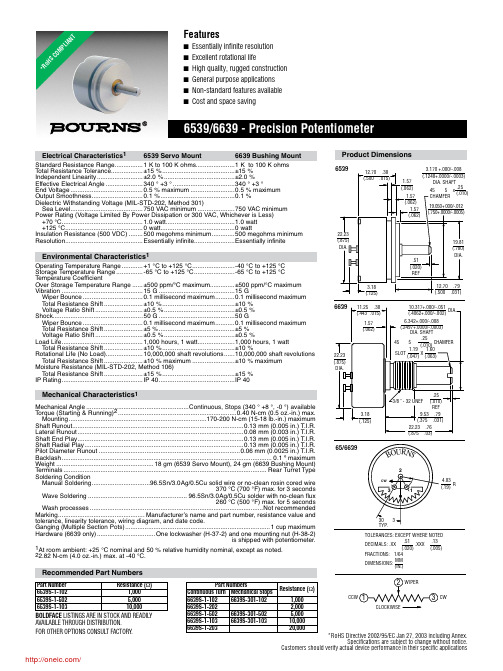
22.23 (.875) DIA.
3.18 (.125)
6639
11.25 .38 (.443 .015)
1.57 (.062)
Байду номын сангаас
22.23 (.875) DIA.
.51 (.020) REF
19.81 (.780) DIA.
12.70 .79 (.500 .031)
10.317+.000/-.051 (.4062+.000/-.002)
DIA.
6.342+.000/-.008
(.2497+.0000/-.0003) DIA. SHAFT .25
45 5 (.010) CHAMFER 1.19 1.60
SLOT (.047) X (.063)
Mechanical Characteristics1
Mechanical Angle ..........................................................Continuous, Stops (340 ° +8 °, -0 °) available Torque (Starting & Running)2 ...................................................................0.40 N-cm (0.5 oz.-in.) max.
Sea Level......................................... 750 VAC minimum .....................750 VAC minimum Power Rating (Voltage Limited By Power Dissipation or 300 VAC, Whichever is Less)
PD810说明书V1.0.3

5 6 7
8
显示内容 测量数据显示区四排 字
电度亮显示区一排小 字
负荷指示图
测量数据标示符
及
Demand、MAX、MIN、AVG
三相不平衡度标识
负载性质 电度量种类指示 Imp,Total,Net,Exp
■
■
电度
最 值 设定的时间区 三相电流、有功、
■
■
■
统计 间内的最 大 值 无功及视在功率
最小值平均值
电 三相不平衡度
■
■
力 电压电流谐波畸变率
品 2~31 次谐波含有率
质
奇/偶次谐波含有率
时 实时时钟
■
■
■
间 仪表运行时间
通讯 RS485 接口
Modbus-RTU 协议 ■
■
■
■
SOE、越限报警、I/O、模拟量变送、双网通讯、电度脉冲输出等功能需选配相应附加模块
能不具备其中的某些功能,请注意参照下表的内容。
PD810 本体主要功能:
功能
参数
PD810-B PD810-T PD810-E PD810-Q
实 相电压
各相及平均
■
■
■
■
时 线电压
各相及平均
■
■
■
■
测 电流
各相及平均、中线
■
■
■
■
量 有功功率
参 无功功率
数
视在功率
各相及三相总 各相及三相总 各相及三相总
二、 功能概述及选型
型号:(BTEQ)根据功能不同
为了满足客户的不同需求,PD810 系列产品分为四个型号:PD810-B(基本型)、PD810-T(分