HT7825中文资料
HT7818中文资料
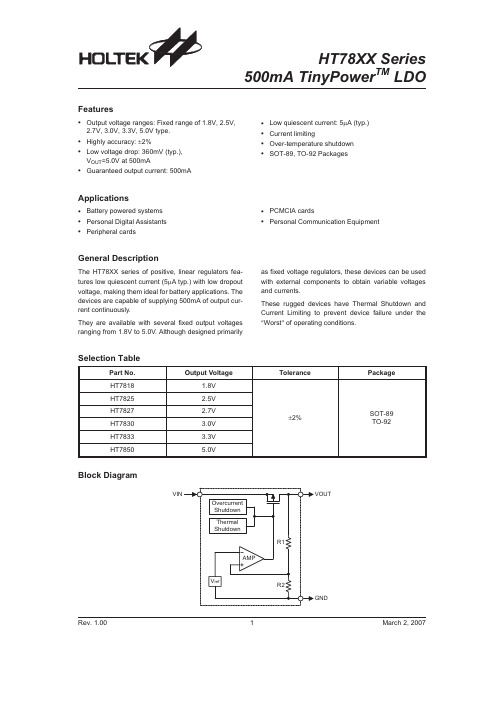
HT78XX Series500mA TinyPower TM LDOSelection TablePart No.Output VoltageTolerancePackageHT7818 1.8V ±2%SOT-89TO-92HT7825 2.5V HT7827 2.7V HT7830 3.0V HT7833 3.3V HT78505.0VBlock DiagramRev.1.001March 2,2007Features·Output voltage ranges:Fixed range of 1.8V,2.5V,2.7V,3.0V,3.3V,5.0V type.·Highly accuracy:±2%·Low voltage drop:360mV (typ.),V OUT =5.0V at 500mA·Guaranteed output current:500mA·Low quiescent current:5m A (typ.)·Current limiting·Over-temperature shutdown ·SOT-89,TO-92PackagesApplications·Battery powered systems ·Personal Digital Assistants ·Peripheral cards·PCMCIA cards·Personal Communication EquipmentGeneral DescriptionThe HT78XX series of positive,linear regulators fea-tures low quiescent current (5m A typ.)with low dropout voltage,making them ideal for battery applications.The devices are capable of supplying 500mA of output cur-rent continuously.They are available with several fixed output voltages ranging from 1.8V to 5.0V.Although designed primarilyas fixed voltage regulators,these devices can be used with external components to obtain variable voltages and currents.These rugged devices have Thermal Shutdown and Current Limiting to prevent device failure under the ²Worst ²of operatingconditions.Pin AssignmentAbsolute Maximum Ratings*Maximum Supply Voltage ............................up to 8.5V Storage Temperature ..........................-50°C to 125°COperating Temperature .........................-40°C to 85°CNote:These are stress ratings only.Stresses exceeding the range specified under ²Absolute Maximum Ratings ²maycause substantial damage to the device.Functional operation of this device at other conditions beyond those listed in the specification is not implied and prolonged exposure to extreme conditions may affect device reliability.²*²Absolute maximum ratings indicate limits beyond which damage to the device may occur.Operating Ratings in-dicate conditions for which the device is intended to be functional,but do not guarantee specific performance limits.The guaranteed specifications apply only for the test conditions listed.Thermal InformationSymbolParameterPackage Max.Unit q JAThermal Resistance (Junction to Ambient)(Assume no ambient airflow,no heat sink)SOT-89200°C/W TO-92200°C/W P DPower DissipationSOT-890.50W TO-920.50WNote:P D is measured at Ta=25°CRev.1.002March 2,2007Electrical Characteristics Tj=25°C,V IN=V OUT+1.0V,I O=1mA,unless otherwise specified Symbol Parameter Test Conditions Min.Typ.Max.UnitV IN Input Voltage¾¾¾8VD V OUT Output Voltage Tolerance¾-2¾2%I SS Quiescent Current I O=0mA¾57m AD V LOAD Load Regulation(Note1)1mA£I OUT£500mA¾0.0040.008%/mAV DROP Dropout Voltage(Note2)D V OUT=2%I OUT=500mAV O£1.8V¾8001200mV2.5V£V O£2.7V¾5006503.0V£V O£5.0V¾360500D V LINE Line Regulation V OUT+1.0V£V IN£8.0V¾0.20.3%/VI LIM Current Limit(Note3)D V OUT=10%500¾¾mATemperature Coefficient-40°C<Ta<85°C¾±0.8¾mV/°C Note: 1.Load regulation is measured at a constant junction temperature,using pulse testing with a low ON time and is guaranteed up to the maximum power dissipation.Power dissipation is determined by the input/outputdifferential voltage and the output current.Guaranteed maximum power dissipation will not be available over the full input/output range.The maximum allowable power dissipation at any ambient temperature isP D=(T J(MAX)-Ta)/q JA.2.Dropout voltage is defined as the input voltage minus the output voltage that produces a2%change in theoutput voltage from the value at V IN=V OUT+1V with a fixed load.3.Current limit is measured by pulsing for a short time.Application CircuitsBasic CircuitsTypical Application Circuits·High output current positive voltage regulatorRev.1.003March2,2007·Increased Output voltage CircuitV=V(1+R2R1)+I R2OUT XX SS ·Dual Supply CircuitV=V+VOUT1XX2XX1V=VOUT2XX2·Tracking Voltage Regulator-V=V x R RO O A BRev.1.004March2,2007Package Information3-Pin SOT-89Outline DimensionsSymbolDimensions in milMin.Nom.Max.A173¾181B64¾72C90¾102D35¾47E155¾167F14¾19G17¾22H¾59¾I55¾63J14¾17Rev.1.005March2,20073-Pin TO-92Outline DimensionsSymbolDimensions in milMin.Nom.Max.A170¾200B170¾200C500¾¾D11¾20E90¾110F45¾55G45¾65H130¾160I8¾18a4°¾6°Rev.1.006March2,2007Product Tape and Reel SpecificationsReel DimensionsSOT-89Symbol Description Dimensions in mmA Reel Outer Diameter180±1.0B Reel Inner Diameter62±1.5C Spindle Hole Diameter12.75+0.15D Key Slit Width 1.9±0.15T1Space Between Flange12.4+0.2T2Reel Thickness17-0.4Rev.1.007March2,2007TO-92Reel Dimensions(Unit:mm)Rev.1.008March2,2007Carrier Tape DimensionsSOT-89Symbol Description Dimensions in mmW Carrier Tape Width 12.0+0.3-0.1P Cavity Pitch8.0±0.1E Perforation Position 1.75±0.1F Cavity to Perforation(Width Direction) 5.5±0.05D Perforation Diameter 1.5+0.1D1Cavity Hole Diameter 1.5+0.1P0Perforation Pitch 4.0±0.1P1Cavity to Perforation(Length Direction) 2.0±0.10A0Cavity Length 4.8±0.1B0Cavity Width 4.5±0.1K0Cavity Depth 1.8±0.1t Carrier Tape Thickness0.30±0.013C Cover Tape Width9.3Rev.1.009March2,2007TO-92Carrier Tape DimensionsTO-92Symbol Description Dimensions in mm I1Taped Lead Length(2.5)P Component Pitch12.7±1.0P0Perforation Pitch12.7±0.3P2Component to Perforation(Length Direction) 6.35±0.4F1Lead Spread 2.5+0.4-0.1F2Lead Spread 2.5+0.4-0.1D h Component Alignment0±0.1W Carrier Tape Width 18.0+1.0-0.5W0Hold-down Tape Width 6.0±0.5W1Perforation Position9.0±0.5W2Hold-down Tape Position(0.5)H0Lead Clinch Height16.0±0.5H1Component Height Less than24.7D0Perforation Diameter 4.0±0.2t Taped Lead Thickness0.7±0.2H Component Base Height19.0±0.5Note:Thickness less than0.38±0.05mm~0.5mmP0Accumulated pitch tolerance:±1mm/20pitches.()Bracketed figures are for consultation onlyRev.1.0010March2,2007HT78XX SeriesRev.1.0011March 2,2007Holtek Semiconductor Inc.(Headquarters)No.3,Creation Rd.II,Science Park,Hsinchu,TaiwanTel:886-3-563-1999Fax:886-3-563-1189Holtek Semiconductor Inc.(Taipei Sales Office)4F-2,No.3-2,YuanQu St.,Nankang Software Park,Taipei 115,TaiwanTel:886-2-2655-7070Fax:886-2-2655-7373Fax:886-2-2655-7383(International sales hotline)Holtek Semiconductor Inc.(Shanghai Sales Office)7th Floor,Building 2,No.889,Yi Shan Rd.,Shanghai,China 200233Tel:86-21-6485-5560Fax:86-21-6485-0313Holtek Semiconductor Inc.(Shenzhen Sales Office)5/F,Unit A,Productivity Building,Cross of Science M 3rd Road and Gaoxin M 2nd Road,Science Park,Nanshan District,Shenzhen,China 518057Tel:86-755-8616-9908,86-755-8616-9308Fax:86-755-8616-9722Holtek Semiconductor Inc.(Beijing Sales Office)Suite 1721,Jinyu Tower,A129West Xuan Wu Men Street,Xicheng District,Beijing,China 100031Tel:86-10-6641-0030,86-10-6641-7751,86-10-6641-7752Fax:86-10-6641-0125Holtek Semiconductor Inc.(Chengdu Sales Office)709,Building 3,Champagne Plaza,No.97Dongda Street,Chengdu,Sichuan,China 610016Tel:86-28-6653-6590Fax:86-28-6653-6591Holtek Semiconductor (USA),Inc.(North America Sales Office)46729Fremont Blvd.,Fremont,CA 94538Tel:1-510-252-9880Fax:1-510-252-9885Copyright Ó2007by HOLTEK SEMICONDUCTOR INC.The information appearing in this Data Sheet is believed to be accurate at the time of publication.However,Holtek as-sumes no responsibility arising from the use of the specifications described.The applications mentioned herein are used solely for the purpose of illustration and Holtek makes no warranty or representation that such applications will be suitable without further modification,nor recommends the use of its products for application that may present a risk to human life due to malfunction or otherwise.Holtek ¢s products are not authorized for use as critical components in life support devices or systems.Holtek reserves the right to alter its products without prior notification.For the most up-to-date information,please visit our web site at .元器件交易网。
装甲车用7a52铝合金焊接性研究

2001 进 行 板 对 接 接 头 横 向 拉 伸 试 验ꎮ 结 果 表 明ꎬ
7A52 铝合金焊接接头的拉伸性能良好ꎬ其抗拉强度
图 2 射线检测结果
Fig.2 Gamma-ray test results
平均达到 274.8 MPaꎬ焊接系数约为 0.58ꎮ 因焊材与
母材为低强度匹配关系ꎬ且强度差异大ꎬ所以试样断
367
19.9
155
333
21.7
156
483
21.7
2.1 焊接接头无损检测
通过目视检测ꎬ7A52 铝合金各种接头类型焊缝
表面成型良好ꎬ 产 生 飞 溅 较 小、 熔 合 情 况 良 好、 无 气
495
25
0
25
0
25
25
25
25
25
25
25
25
0
0
0
0
0
0
0
0
孔、裂纹等焊接缺陷ꎬ焊缝表面状态见图 1ꎮ 按照 ISO
有色金属加工
32
第 49 卷
表 2 7A52 铝合金焊接试验焊接工艺参数
Tab.2 Welding process parameters of 7A52 aluminum alloy welding test
焊接接头类型
试板编号
DJ-1
板对接
焊接电流 / A
焊接电压 / V
焊接速度 / ( mm / min)
气体流量 / ( L / min)
弧长修正
78
17.4
409
25
0
DJ-2
DJ-3
T 型接头
管板
112
GB-1
HT7830中文资料

HT78XX Series500mA TinyPower TM LDOSelection TablePart No.Output VoltageTolerancePackageHT7818 1.8V ±2%SOT-89TO-92HT7825 2.5V HT7827 2.7V HT7830 3.0V HT7833 3.3V HT78505.0VBlock DiagramRev.1.001March 2,2007Features·Output voltage ranges:Fixed range of 1.8V,2.5V,2.7V,3.0V,3.3V,5.0V type.·Highly accuracy:±2%·Low voltage drop:360mV (typ.),V OUT =5.0V at 500mA·Guaranteed output current:500mA·Low quiescent current:5m A (typ.)·Current limiting·Over-temperature shutdown ·SOT-89,TO-92PackagesApplications·Battery powered systems ·Personal Digital Assistants ·Peripheral cards·PCMCIA cards·Personal Communication EquipmentGeneral DescriptionThe HT78XX series of positive,linear regulators fea-tures low quiescent current (5m A typ.)with low dropout voltage,making them ideal for battery applications.The devices are capable of supplying 500mA of output cur-rent continuously.They are available with several fixed output voltages ranging from 1.8V to 5.0V.Although designed primarilyas fixed voltage regulators,these devices can be used with external components to obtain variable voltages and currents.These rugged devices have Thermal Shutdown and Current Limiting to prevent device failure under the ²Worst ²of operatingconditions.Pin AssignmentAbsolute Maximum Ratings*Maximum Supply Voltage ............................up to 8.5V Storage Temperature ..........................-50°C to 125°COperating Temperature .........................-40°C to 85°CNote:These are stress ratings only.Stresses exceeding the range specified under ²Absolute Maximum Ratings ²maycause substantial damage to the device.Functional operation of this device at other conditions beyond those listed in the specification is not implied and prolonged exposure to extreme conditions may affect device reliability.²*²Absolute maximum ratings indicate limits beyond which damage to the device may occur.Operating Ratings in-dicate conditions for which the device is intended to be functional,but do not guarantee specific performance limits.The guaranteed specifications apply only for the test conditions listed.Thermal InformationSymbolParameterPackage Max.Unit q JAThermal Resistance (Junction to Ambient)(Assume no ambient airflow,no heat sink)SOT-89200°C/W TO-92200°C/W P DPower DissipationSOT-890.50W TO-920.50WNote:P D is measured at Ta=25°CRev.1.002March 2,2007Electrical Characteristics Tj=25°C,V IN=V OUT+1.0V,I O=1mA,unless otherwise specified Symbol Parameter Test Conditions Min.Typ.Max.UnitV IN Input Voltage¾¾¾8VD V OUT Output Voltage Tolerance¾-2¾2%I SS Quiescent Current I O=0mA¾57m AD V LOAD Load Regulation(Note1)1mA£I OUT£500mA¾0.0040.008%/mAV DROP Dropout Voltage(Note2)D V OUT=2%I OUT=500mAV O£1.8V¾8001200mV2.5V£V O£2.7V¾5006503.0V£V O£5.0V¾360500D V LINE Line Regulation V OUT+1.0V£V IN£8.0V¾0.20.3%/VI LIM Current Limit(Note3)D V OUT=10%500¾¾mATemperature Coefficient-40°C<Ta<85°C¾±0.8¾mV/°C Note: 1.Load regulation is measured at a constant junction temperature,using pulse testing with a low ON time and is guaranteed up to the maximum power dissipation.Power dissipation is determined by the input/outputdifferential voltage and the output current.Guaranteed maximum power dissipation will not be available over the full input/output range.The maximum allowable power dissipation at any ambient temperature isP D=(T J(MAX)-Ta)/q JA.2.Dropout voltage is defined as the input voltage minus the output voltage that produces a2%change in theoutput voltage from the value at V IN=V OUT+1V with a fixed load.3.Current limit is measured by pulsing for a short time.Application CircuitsBasic CircuitsTypical Application Circuits·High output current positive voltage regulatorRev.1.003March2,2007·Increased Output voltage CircuitV=V(1+R2R1)+I R2OUT XX SS ·Dual Supply CircuitV=V+VOUT1XX2XX1V=VOUT2XX2·Tracking Voltage Regulator-V=V x R RO O A BRev.1.004March2,2007Package Information3-Pin SOT-89Outline DimensionsSymbolDimensions in milMin.Nom.Max.A173¾181B64¾72C90¾102D35¾47E155¾167F14¾19G17¾22H¾59¾I55¾63J14¾17Rev.1.005March2,20073-Pin TO-92Outline DimensionsSymbolDimensions in milMin.Nom.Max.A170¾200B170¾200C500¾¾D11¾20E90¾110F45¾55G45¾65H130¾160I8¾18a4°¾6°Rev.1.006March2,2007Product Tape and Reel SpecificationsReel DimensionsSOT-89Symbol Description Dimensions in mmA Reel Outer Diameter180±1.0B Reel Inner Diameter62±1.5C Spindle Hole Diameter12.75+0.15D Key Slit Width 1.9±0.15T1Space Between Flange12.4+0.2T2Reel Thickness17-0.4Rev.1.007March2,2007TO-92Reel Dimensions(Unit:mm)Rev.1.008March2,2007Carrier Tape DimensionsSOT-89Symbol Description Dimensions in mmW Carrier Tape Width 12.0+0.3-0.1P Cavity Pitch8.0±0.1E Perforation Position 1.75±0.1F Cavity to Perforation(Width Direction) 5.5±0.05D Perforation Diameter 1.5+0.1D1Cavity Hole Diameter 1.5+0.1P0Perforation Pitch 4.0±0.1P1Cavity to Perforation(Length Direction) 2.0±0.10A0Cavity Length 4.8±0.1B0Cavity Width 4.5±0.1K0Cavity Depth 1.8±0.1t Carrier Tape Thickness0.30±0.013C Cover Tape Width9.3Rev.1.009March2,2007TO-92Carrier Tape DimensionsTO-92Symbol Description Dimensions in mm I1Taped Lead Length(2.5)P Component Pitch12.7±1.0P0Perforation Pitch12.7±0.3P2Component to Perforation(Length Direction) 6.35±0.4F1Lead Spread 2.5+0.4-0.1F2Lead Spread 2.5+0.4-0.1D h Component Alignment0±0.1W Carrier Tape Width 18.0+1.0-0.5W0Hold-down Tape Width 6.0±0.5W1Perforation Position9.0±0.5W2Hold-down Tape Position(0.5)H0Lead Clinch Height16.0±0.5H1Component Height Less than24.7D0Perforation Diameter 4.0±0.2t Taped Lead Thickness0.7±0.2H Component Base Height19.0±0.5Note:Thickness less than0.38±0.05mm~0.5mmP0Accumulated pitch tolerance:±1mm/20pitches.()Bracketed figures are for consultation onlyRev.1.0010March2,2007HT78XX SeriesRev.1.0011March 2,2007Holtek Semiconductor Inc.(Headquarters)No.3,Creation Rd.II,Science Park,Hsinchu,TaiwanTel:886-3-563-1999Fax:886-3-563-1189Holtek Semiconductor Inc.(Taipei Sales Office)4F-2,No.3-2,YuanQu St.,Nankang Software Park,Taipei 115,TaiwanTel:886-2-2655-7070Fax:886-2-2655-7373Fax:886-2-2655-7383(International sales hotline)Holtek Semiconductor Inc.(Shanghai Sales Office)7th Floor,Building 2,No.889,Yi Shan Rd.,Shanghai,China 200233Tel:86-21-6485-5560Fax:86-21-6485-0313Holtek Semiconductor Inc.(Shenzhen Sales Office)5/F,Unit A,Productivity Building,Cross of Science M 3rd Road and Gaoxin M 2nd Road,Science Park,Nanshan District,Shenzhen,China 518057Tel:86-755-8616-9908,86-755-8616-9308Fax:86-755-8616-9722Holtek Semiconductor Inc.(Beijing Sales Office)Suite 1721,Jinyu Tower,A129West Xuan Wu Men Street,Xicheng District,Beijing,China 100031Tel:86-10-6641-0030,86-10-6641-7751,86-10-6641-7752Fax:86-10-6641-0125Holtek Semiconductor Inc.(Chengdu Sales Office)709,Building 3,Champagne Plaza,No.97Dongda Street,Chengdu,Sichuan,China 610016Tel:86-28-6653-6590Fax:86-28-6653-6591Holtek Semiconductor (USA),Inc.(North America Sales Office)46729Fremont Blvd.,Fremont,CA 94538Tel:1-510-252-9880Fax:1-510-252-9885Copyright Ó2007by HOLTEK SEMICONDUCTOR INC.The information appearing in this Data Sheet is believed to be accurate at the time of publication.However,Holtek as-sumes no responsibility arising from the use of the specifications described.The applications mentioned herein are used solely for the purpose of illustration and Holtek makes no warranty or representation that such applications will be suitable without further modification,nor recommends the use of its products for application that may present a risk to human life due to malfunction or otherwise.Holtek ¢s products are not authorized for use as critical components in life support devices or systems.Holtek reserves the right to alter its products without prior notification.For the most up-to-date information,please visit our web site at .元器件交易网。
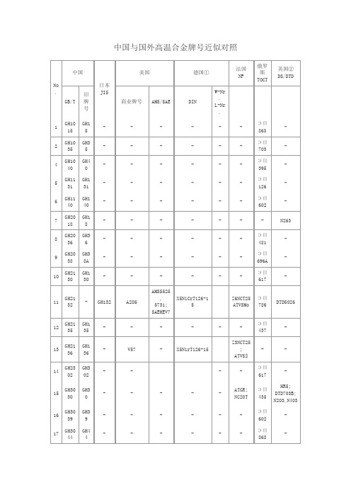
中国与国外高温合金铸造高温合金和耐蚀合金牌近似对照
N80A
20
GH4037
GH37
-
-
AMS5829;
SAEHEV6;
-
-
ATGS4;
NC20KTA
ЭП617
2HRC,
2HR202
DTD747B;
N501,N503
21
GH4043
GH43
-
-
-
-
-
-ЭП598
-
-
22
GH4049
GH49
-
-
-
-
NCK15
ATD
ЭП929
HR4;
N115
ATGX
Z12CNKDW20
-
-
26
-
GH20
NCF800B;
NCF2B
Incoloy800
AMS5766,
5871;
X10NiCrAlTi32-20
25NC35-20;
NicralC
-
Incoloy800
27
-
GH32
-
HestelloyX
AMS5536
5754;
SG-NiCr21Fe18Mo
ATGE
中国与国外高温合金牌号近似对照
No.
中国
日本
JIS
美国
德国①
法国
NF
俄罗斯
TOCT
英国②
DS/DTD
GB/T
旧牌号
商业牌号
AMS/SAE
DIN
W-Nr.
L-Nr.
1
GH1015
GH15
-
-
-
-
-
-
AC7815子系列数据手册
1 主要特性 .................................................................................................................. 5
2 器件标识 ......................................................................................................................................... 6
Page 3 of 32
本文档包含信息归 AutoChips 所有,未经许可,严禁转载或披露
AC7815 数据手册
6.2.2 内部 RC 特性 ...................................................................................................... 17 6.2.3 PLL 特性 ............................................................................................................. 17 6.3 片内 Flash 规格................................................................................................................... 18 6.4 模拟..................................................................................................................................... 18 6.4.1 ADC 特性............................................................................................................ 18 6.4.2 模拟比较器(ACMP)电气规格 ......................................................................... 19 6.5 通信接口 ............................................................................................................................. 20 6.5.1 SPI 开关规格 ...................................................................................................... 20 6.5.2 CAN 特性 ............................................................................................................ 22 7 尺寸 .............................................................................................................................................. 23 7.1 LQFP64 封装信息 ............................................................................................................... 23 7.2 LQFP80 封装信息 ............................................................................................................... 25 8 引脚分配 ....................................................................................................................................... 28 8.1 信号多路复用和引脚分配 .................................................................................................... 28 8.2 器件引脚分配 ...................................................................................................................... 31
HT 规格书
•低压降•较低的温度系数•高输入电压 (高达 30V)•静态电流 2.5μA•大电流输出:100mA•输出电压精度:±3%•封装类型:TO92, SOT89 和 SOT23-5应用领域•电池供电设备•通信设备•音频/视频设备功耗高电压稳压器。
输出电流为 100mA 且允许的输入电压可高达 30V。
具有几个固定的输出电压,范围从 2.1V 到 12.0V。
CMOS 技术可确保其具有低压降和低静态电流的特性。
尽管主要为固定电压调节器而设计,但这些 IC 可与外部元件结合来获得可变的电压和电流。
注:“xx”代表输出电压。
Rev. 2.3012014-03-19引脚图极限参数工作环境温度 .................................................−40°C ~ 85°C 电源供应电压 ...................................................−0.3V ~ 33V储存温度范围 ...............................................−50°C ~ 125°C注:这里只强调额定功率,超过极限参数所规定的范围将对芯片造成损害,无法预期芯片在上述标示范围外的工作状态,而且若长期在标示范围外的条件下工作,可能影响芯片的可靠性。
热能信息Rev. 2.3022014-03-19电气特性HT7521-1, +2.1V 输出类型注:在 V IN = V OUT+2V 与一个固定负载条件下使输出电压下降 2%,此时的输入电压减去输出电压就是Dropout 电压。
HT7523-1, +2.3V 输出类型注:在 V IN = V OUT+2V 与一个固定负载条件下使输出电压下降 2%,此时的输入电压减去输出电压就是Dropout 电压。
Rev. 2.3032014-03-19注:在 V IN = V OUT+2V 与一个固定负载条件下使输出电压下降 2%,此时的输入电压减去输出电压就是Dropout 电压。
HT7850中文资料

HT78XX Series500mA TinyPower TM LDOSelection TablePart No.Output VoltageTolerancePackageHT7818 1.8V ±2%SOT-89TO-92HT7825 2.5V HT7827 2.7V HT7830 3.0V HT7833 3.3V HT78505.0VBlock DiagramRev.1.001March 2,2007Features·Output voltage ranges:Fixed range of 1.8V,2.5V,2.7V,3.0V,3.3V,5.0V type.·Highly accuracy:±2%·Low voltage drop:360mV (typ.),V OUT =5.0V at 500mA·Guaranteed output current:500mA·Low quiescent current:5m A (typ.)·Current limiting·Over-temperature shutdown ·SOT-89,TO-92PackagesApplications·Battery powered systems ·Personal Digital Assistants ·Peripheral cards·PCMCIA cards·Personal Communication EquipmentGeneral DescriptionThe HT78XX series of positive,linear regulators fea-tures low quiescent current (5m A typ.)with low dropout voltage,making them ideal for battery applications.The devices are capable of supplying 500mA of output cur-rent continuously.They are available with several fixed output voltages ranging from 1.8V to 5.0V.Although designed primarilyas fixed voltage regulators,these devices can be used with external components to obtain variable voltages and currents.These rugged devices have Thermal Shutdown and Current Limiting to prevent device failure under the ²Worst ²of operatingconditions.Pin AssignmentAbsolute Maximum Ratings*Maximum Supply Voltage ............................up to 8.5V Storage Temperature ..........................-50°C to 125°COperating Temperature .........................-40°C to 85°CNote:These are stress ratings only.Stresses exceeding the range specified under ²Absolute Maximum Ratings ²maycause substantial damage to the device.Functional operation of this device at other conditions beyond those listed in the specification is not implied and prolonged exposure to extreme conditions may affect device reliability.²*²Absolute maximum ratings indicate limits beyond which damage to the device may occur.Operating Ratings in-dicate conditions for which the device is intended to be functional,but do not guarantee specific performance limits.The guaranteed specifications apply only for the test conditions listed.Thermal InformationSymbolParameterPackage Max.Unit q JAThermal Resistance (Junction to Ambient)(Assume no ambient airflow,no heat sink)SOT-89200°C/W TO-92200°C/W P DPower DissipationSOT-890.50W TO-920.50WNote:P D is measured at Ta=25°CRev.1.002March 2,2007Electrical Characteristics Tj=25°C,V IN=V OUT+1.0V,I O=1mA,unless otherwise specified Symbol Parameter Test Conditions Min.Typ.Max.UnitV IN Input Voltage¾¾¾8VD V OUT Output Voltage Tolerance¾-2¾2%I SS Quiescent Current I O=0mA¾57m AD V LOAD Load Regulation(Note1)1mA£I OUT£500mA¾0.0040.008%/mAV DROP Dropout Voltage(Note2)D V OUT=2%I OUT=500mAV O£1.8V¾8001200mV2.5V£V O£2.7V¾5006503.0V£V O£5.0V¾360500D V LINE Line Regulation V OUT+1.0V£V IN£8.0V¾0.20.3%/VI LIM Current Limit(Note3)D V OUT=10%500¾¾mATemperature Coefficient-40°C<Ta<85°C¾±0.8¾mV/°C Note: 1.Load regulation is measured at a constant junction temperature,using pulse testing with a low ON time and is guaranteed up to the maximum power dissipation.Power dissipation is determined by the input/outputdifferential voltage and the output current.Guaranteed maximum power dissipation will not be available over the full input/output range.The maximum allowable power dissipation at any ambient temperature isP D=(T J(MAX)-Ta)/q JA.2.Dropout voltage is defined as the input voltage minus the output voltage that produces a2%change in theoutput voltage from the value at V IN=V OUT+1V with a fixed load.3.Current limit is measured by pulsing for a short time.Application CircuitsBasic CircuitsTypical Application Circuits·High output current positive voltage regulatorRev.1.003March2,2007·Increased Output voltage CircuitV=V(1+R2R1)+I R2OUT XX SS ·Dual Supply CircuitV=V+VOUT1XX2XX1V=VOUT2XX2·Tracking Voltage Regulator-V=V x R RO O A BRev.1.004March2,2007Package Information3-Pin SOT-89Outline DimensionsSymbolDimensions in milMin.Nom.Max.A173¾181B64¾72C90¾102D35¾47E155¾167F14¾19G17¾22H¾59¾I55¾63J14¾17Rev.1.005March2,20073-Pin TO-92Outline DimensionsSymbolDimensions in milMin.Nom.Max.A170¾200B170¾200C500¾¾D11¾20E90¾110F45¾55G45¾65H130¾160I8¾18a4°¾6°Rev.1.006March2,2007Product Tape and Reel SpecificationsReel DimensionsSOT-89Symbol Description Dimensions in mmA Reel Outer Diameter180±1.0B Reel Inner Diameter62±1.5C Spindle Hole Diameter12.75+0.15D Key Slit Width 1.9±0.15T1Space Between Flange12.4+0.2T2Reel Thickness17-0.4Rev.1.007March2,2007TO-92Reel Dimensions(Unit:mm)Rev.1.008March2,2007Carrier Tape DimensionsSOT-89Symbol Description Dimensions in mmW Carrier Tape Width 12.0+0.3-0.1P Cavity Pitch8.0±0.1E Perforation Position 1.75±0.1F Cavity to Perforation(Width Direction) 5.5±0.05D Perforation Diameter 1.5+0.1D1Cavity Hole Diameter 1.5+0.1P0Perforation Pitch 4.0±0.1P1Cavity to Perforation(Length Direction) 2.0±0.10A0Cavity Length 4.8±0.1B0Cavity Width 4.5±0.1K0Cavity Depth 1.8±0.1t Carrier Tape Thickness0.30±0.013C Cover Tape Width9.3Rev.1.009March2,2007TO-92Carrier Tape DimensionsTO-92Symbol Description Dimensions in mm I1Taped Lead Length(2.5)P Component Pitch12.7±1.0P0Perforation Pitch12.7±0.3P2Component to Perforation(Length Direction) 6.35±0.4F1Lead Spread 2.5+0.4-0.1F2Lead Spread 2.5+0.4-0.1D h Component Alignment0±0.1W Carrier Tape Width 18.0+1.0-0.5W0Hold-down Tape Width 6.0±0.5W1Perforation Position9.0±0.5W2Hold-down Tape Position(0.5)H0Lead Clinch Height16.0±0.5H1Component Height Less than24.7D0Perforation Diameter 4.0±0.2t Taped Lead Thickness0.7±0.2H Component Base Height19.0±0.5Note:Thickness less than0.38±0.05mm~0.5mmP0Accumulated pitch tolerance:±1mm/20pitches.()Bracketed figures are for consultation onlyRev.1.0010March2,2007HT78XX SeriesRev.1.0011March 2,2007Holtek Semiconductor Inc.(Headquarters)No.3,Creation Rd.II,Science Park,Hsinchu,TaiwanTel:886-3-563-1999Fax:886-3-563-1189Holtek Semiconductor Inc.(Taipei Sales Office)4F-2,No.3-2,YuanQu St.,Nankang Software Park,Taipei 115,TaiwanTel:886-2-2655-7070Fax:886-2-2655-7373Fax:886-2-2655-7383(International sales hotline)Holtek Semiconductor Inc.(Shanghai Sales Office)7th Floor,Building 2,No.889,Yi Shan Rd.,Shanghai,China 200233Tel:86-21-6485-5560Fax:86-21-6485-0313Holtek Semiconductor Inc.(Shenzhen Sales Office)5/F,Unit A,Productivity Building,Cross of Science M 3rd Road and Gaoxin M 2nd Road,Science Park,Nanshan District,Shenzhen,China 518057Tel:86-755-8616-9908,86-755-8616-9308Fax:86-755-8616-9722Holtek Semiconductor Inc.(Beijing Sales Office)Suite 1721,Jinyu Tower,A129West Xuan Wu Men Street,Xicheng District,Beijing,China 100031Tel:86-10-6641-0030,86-10-6641-7751,86-10-6641-7752Fax:86-10-6641-0125Holtek Semiconductor Inc.(Chengdu Sales Office)709,Building 3,Champagne Plaza,No.97Dongda Street,Chengdu,Sichuan,China 610016Tel:86-28-6653-6590Fax:86-28-6653-6591Holtek Semiconductor (USA),Inc.(North America Sales Office)46729Fremont Blvd.,Fremont,CA 94538Tel:1-510-252-9880Fax:1-510-252-9885Copyright Ó2007by HOLTEK SEMICONDUCTOR INC.The information appearing in this Data Sheet is believed to be accurate at the time of publication.However,Holtek as-sumes no responsibility arising from the use of the specifications described.The applications mentioned herein are used solely for the purpose of illustration and Holtek makes no warranty or representation that such applications will be suitable without further modification,nor recommends the use of its products for application that may present a risk to human life due to malfunction or otherwise.Holtek ¢s products are not authorized for use as critical components in life support devices or systems.Holtek reserves the right to alter its products without prior notification.For the most up-to-date information,please visit our web site at .元器件交易网。
78D05中文资料

Vo
Iq DIq DIq VN DVo/DT RR IPK ISC Vd
56
58 -1.1 72 1.2 250 2.0
Contek Microelectronics Co.,Ltd.
CONTEK
E-mail:sales@
3
MIN
8.65 8.6
TYP
9.00
MAX
9.35 9.4 90 45 90 90 8.0 1.0 0.5
UNIT
V V mV mV mV mV mA mA mA uV mV/ C dB A mA V
Quiescent Current Quiescent Current Change Output Noise Voltage Temperature coefficient of Ripple Rejection Peak Output Current Short-Circuit Current Dropout Voltage
MIN
4.8 4.75
TYP
5.0
MAX
5.2 5.25 50 25 50 50 8.0 1.0 0.5
UNIT
V V mV mV mV mV mA mA mA uV mV/ C dB A mA V
62
40 -0.6 80 1.2 250 2.0
Contek78D06 ELECTRICAL CHARACTERISTICS
MIN
TYP
1.2 250 2.0
MAX
UNIT
A mA V
Contek78D08 ELECTRICAL CHARACTERISTICS
PARAMETER
Output Voltage Load Regulation Line regulation Quiescent Current Quiescent Current Change Output Noise Voltage Temperature coefficient of Ripple Rejection Peak Output Current Short-Circuit Current Dropout Voltage
- 1、下载文档前请自行甄别文档内容的完整性,平台不提供额外的编辑、内容补充、找答案等附加服务。
- 2、"仅部分预览"的文档,不可在线预览部分如存在完整性等问题,可反馈申请退款(可完整预览的文档不适用该条件!)。
- 3、如文档侵犯您的权益,请联系客服反馈,我们会尽快为您处理(人工客服工作时间:9:00-18:30)。
HT78XX Series500mA TinyPower TM LDOSelection TablePart No.Output VoltageTolerancePackageHT7818 1.8V ±2%SOT-89TO-92HT7825 2.5V HT7827 2.7V HT7830 3.0V HT7833 3.3V HT78505.0VBlock DiagramRev.1.001March 2,2007Features·Output voltage ranges:Fixed range of 1.8V,2.5V,2.7V,3.0V,3.3V,5.0V type.·Highly accuracy:±2%·Low voltage drop:360mV (typ.),V OUT =5.0V at 500mA·Guaranteed output current:500mA·Low quiescent current:5m A (typ.)·Current limiting·Over-temperature shutdown ·SOT-89,TO-92PackagesApplications·Battery powered systems ·Personal Digital Assistants ·Peripheral cards·PCMCIA cards·Personal Communication EquipmentGeneral DescriptionThe HT78XX series of positive,linear regulators fea-tures low quiescent current (5m A typ.)with low dropout voltage,making them ideal for battery applications.The devices are capable of supplying 500mA of output cur-rent continuously.They are available with several fixed output voltages ranging from 1.8V to 5.0V.Although designed primarilyas fixed voltage regulators,these devices can be used with external components to obtain variable voltages and currents.These rugged devices have Thermal Shutdown and Current Limiting to prevent device failure under the ²Worst ²of operatingconditions.Pin AssignmentAbsolute Maximum Ratings*Maximum Supply Voltage ............................up to 8.5V Storage Temperature ..........................-50°C to 125°COperating Temperature .........................-40°C to 85°CNote:These are stress ratings only.Stresses exceeding the range specified under ²Absolute Maximum Ratings ²maycause substantial damage to the device.Functional operation of this device at other conditions beyond those listed in the specification is not implied and prolonged exposure to extreme conditions may affect device reliability.²*²Absolute maximum ratings indicate limits beyond which damage to the device may occur.Operating Ratings in-dicate conditions for which the device is intended to be functional,but do not guarantee specific performance limits.The guaranteed specifications apply only for the test conditions listed.Thermal InformationSymbolParameterPackage Max.Unit q JAThermal Resistance (Junction to Ambient)(Assume no ambient airflow,no heat sink)SOT-89200°C/W TO-92200°C/W P DPower DissipationSOT-890.50W TO-920.50WNote:P D is measured at Ta=25°CRev.1.002March 2,2007Electrical Characteristics Tj=25°C,V IN=V OUT+1.0V,I O=1mA,unless otherwise specified Symbol Parameter Test Conditions Min.Typ.Max.UnitV IN Input Voltage¾¾¾8VD V OUT Output Voltage Tolerance¾-2¾2%I SS Quiescent Current I O=0mA¾57m AD V LOAD Load Regulation(Note1)1mA£I OUT£500mA¾0.0040.008%/mAV DROP Dropout Voltage(Note2)D V OUT=2%I OUT=500mAV O£1.8V¾8001200mV2.5V£V O£2.7V¾5006503.0V£V O£5.0V¾360500D V LINE Line Regulation V OUT+1.0V£V IN£8.0V¾0.20.3%/VI LIM Current Limit(Note3)D V OUT=10%500¾¾mATemperature Coefficient-40°C<Ta<85°C¾±0.8¾mV/°C Note: 1.Load regulation is measured at a constant junction temperature,using pulse testing with a low ON time and is guaranteed up to the maximum power dissipation.Power dissipation is determined by the input/outputdifferential voltage and the output current.Guaranteed maximum power dissipation will not be available over the full input/output range.The maximum allowable power dissipation at any ambient temperature isP D=(T J(MAX)-Ta)/q JA.2.Dropout voltage is defined as the input voltage minus the output voltage that produces a2%change in theoutput voltage from the value at V IN=V OUT+1V with a fixed load.3.Current limit is measured by pulsing for a short time.Application CircuitsBasic CircuitsTypical Application Circuits·High output current positive voltage regulatorRev.1.003March2,2007·Increased Output voltage CircuitV=V(1+R2R1)+I R2OUT XX SS ·Dual Supply CircuitV=V+VOUT1XX2XX1V=VOUT2XX2·Tracking Voltage Regulator-V=V x R RO O A BRev.1.004March2,2007Package Information3-Pin SOT-89Outline DimensionsSymbolDimensions in milMin.Nom.Max.A173¾181B64¾72C90¾102D35¾47E155¾167F14¾19G17¾22H¾59¾I55¾63J14¾17Rev.1.005March2,20073-Pin TO-92Outline DimensionsSymbolDimensions in milMin.Nom.Max.A170¾200B170¾200C500¾¾D11¾20E90¾110F45¾55G45¾65H130¾160I8¾18a4°¾6°Rev.1.006March2,2007Product Tape and Reel SpecificationsReel DimensionsSOT-89Symbol Description Dimensions in mmA Reel Outer Diameter180±1.0B Reel Inner Diameter62±1.5C Spindle Hole Diameter12.75+0.15D Key Slit Width 1.9±0.15T1Space Between Flange12.4+0.2T2Reel Thickness17-0.4Rev.1.007March2,2007TO-92Reel Dimensions(Unit:mm)Rev.1.008March2,2007Carrier Tape DimensionsSOT-89Symbol Description Dimensions in mmW Carrier Tape Width 12.0+0.3-0.1P Cavity Pitch8.0±0.1E Perforation Position 1.75±0.1F Cavity to Perforation(Width Direction) 5.5±0.05D Perforation Diameter 1.5+0.1D1Cavity Hole Diameter 1.5+0.1P0Perforation Pitch 4.0±0.1P1Cavity to Perforation(Length Direction) 2.0±0.10A0Cavity Length 4.8±0.1B0Cavity Width 4.5±0.1K0Cavity Depth 1.8±0.1t Carrier Tape Thickness0.30±0.013C Cover Tape Width9.3Rev.1.009March2,2007TO-92Carrier Tape DimensionsTO-92Symbol Description Dimensions in mm I1Taped Lead Length(2.5)P Component Pitch12.7±1.0P0Perforation Pitch12.7±0.3P2Component to Perforation(Length Direction) 6.35±0.4F1Lead Spread 2.5+0.4-0.1F2Lead Spread 2.5+0.4-0.1D h Component Alignment0±0.1W Carrier Tape Width 18.0+1.0-0.5W0Hold-down Tape Width 6.0±0.5W1Perforation Position9.0±0.5W2Hold-down Tape Position(0.5)H0Lead Clinch Height16.0±0.5H1Component Height Less than24.7D0Perforation Diameter 4.0±0.2t Taped Lead Thickness0.7±0.2H Component Base Height19.0±0.5Note:Thickness less than0.38±0.05mm~0.5mmP0Accumulated pitch tolerance:±1mm/20pitches.()Bracketed figures are for consultation onlyRev.1.0010March2,2007HT78XX SeriesRev.1.0011March 2,2007Holtek Semiconductor Inc.(Headquarters)No.3,Creation Rd.II,Science Park,Hsinchu,TaiwanTel:886-3-563-1999Fax:886-3-563-1189Holtek Semiconductor Inc.(Taipei Sales Office)4F-2,No.3-2,YuanQu St.,Nankang Software Park,Taipei 115,TaiwanTel:886-2-2655-7070Fax:886-2-2655-7373Fax:886-2-2655-7383(International sales hotline)Holtek Semiconductor Inc.(Shanghai Sales Office)7th Floor,Building 2,No.889,Yi Shan Rd.,Shanghai,China 200233Tel:86-21-6485-5560Fax:86-21-6485-0313Holtek Semiconductor Inc.(Shenzhen Sales Office)5/F,Unit A,Productivity Building,Cross of Science M 3rd Road and Gaoxin M 2nd Road,Science Park,Nanshan District,Shenzhen,China 518057Tel:86-755-8616-9908,86-755-8616-9308Fax:86-755-8616-9722Holtek Semiconductor Inc.(Beijing Sales Office)Suite 1721,Jinyu Tower,A129West Xuan Wu Men Street,Xicheng District,Beijing,China 100031Tel:86-10-6641-0030,86-10-6641-7751,86-10-6641-7752Fax:86-10-6641-0125Holtek Semiconductor Inc.(Chengdu Sales Office)709,Building 3,Champagne Plaza,No.97Dongda Street,Chengdu,Sichuan,China 610016Tel:86-28-6653-6590Fax:86-28-6653-6591Holtek Semiconductor (USA),Inc.(North America Sales Office)46729Fremont Blvd.,Fremont,CA 94538Tel:1-510-252-9880Fax:1-510-252-9885Copyright Ó2007by HOLTEK SEMICONDUCTOR INC.The information appearing in this Data Sheet is believed to be accurate at the time of publication.However,Holtek as-sumes no responsibility arising from the use of the specifications described.The applications mentioned herein are used solely for the purpose of illustration and Holtek makes no warranty or representation that such applications will be suitable without further modification,nor recommends the use of its products for application that may present a risk to human life due to malfunction or otherwise.Holtek ¢s products are not authorized for use as critical components in life support devices or systems.Holtek reserves the right to alter its products without prior notification.For the most up-to-date information,please visit our web site at .元器件交易网。