NT90RHCDAC12VCB0.6中文资料
数据手册中文版

14位, 165M SPA(采样率)DAC(数模转换器)特性:●单电源供电+5V或+3V●高SFDR (无杂散动态范围): 在100MSPS 64dBc时20MHz输出●低干扰: 3PV -S●低功耗: 170MW (+5 V时)应用●通讯传输通道WLL , 蜂窝基站数字微波链路电缆调制解调器●波形产生直接数字频率合成器(DDS )任意波形发生器(ARB )●医疗/超声●高速仪表和控制●视频, 数字电视说明:DAC904是一款高速数模转换器, 14位分辨率, 引脚兼容DAC908、DAC900、DAC902, 分别提供8-, 10-, 12-位分辨率选择。
该系列DAC支持的所有型号更新率超过165MSPS, 具有优良的动态性能。
DAC904先进分割架构的优化为单音和多频音信号提供高无杂散动态范围(SFDR), 特别是用于通信系统的发送信号电路时。
DAC904具有高阻抗(200KΩ)的电流输出, 标称范围为20mA和一个最多为1.25V的输出。
差分输出允许两个差分或单端模拟信号的接口。
电流输出的匹配保证在差分结构中杰出的动态性能, 它可以与变压器配合使用。
运用一个小的几何CMOS工艺, 单片DAC904可以用在+2.7 V至+5.5 V宽的单电源范围内操作。
其低功耗特性允许它使用在便携式和电池供电系统情况下。
可通过减少输出电流与调整满量程选项实现进一步优化。
DAC904不断运转时, 掉电模式导致其待机功率仅为为45mW 。
DAC904带有一个集成的1.24V带隙基准和边沿触发输入锁存器, 提供完整的转换器解决方案。
+3 V和+5 V CMOS逻辑系列都可以接口到DAC904 。
DAC904的参考结构允许使用芯片上的参考, 或施加外部参考。
通过一个外部电阻, 满量程输出电流可以调整在2 - 20mA, 并保持其指定的动态性能。
DAC904采用SO -28和TSSOP -28封装。
绝对最大额定值+VA到AGND(模拟信号地)......-0.3V至+6V+VD到DGND(数字信号地)......-0.3V到+6VAGND到DGND......-0.3V到+0.3V+VA 到+VD......-6V到+6VCLK, PD到DGND......-0.3V到VD+0.3VD0-D13到DGND......-0.3V到VD+0.3VIOUT, I 到AGND......-1V到VA+0.3VBW,BYP到AGND......-0.3V到VA+0.3VREFIN ,FSA到AGND......-0.3V到VA+0.3VINT/EXT到AGND......-0.3V到VA+0.3V结温度. . . . . . . +150℃存储器温度. . . . . . +125℃防静电敏感度这种集成的电路可以被ESD(静电释放)损坏。
FQA9N90C中文资料

BVDSS ∆BVDSS / ∆TJ
Drain-Source Breakdown Voltage
Breakdown Voltage Temperature Coefficient
VGS = 0 V, ID = 250 µA
900 --
ID = 250 µA, Referenced to 25°C -- 0.99
-55 to +150
300
Typ
Max
--
0.45
0.24
--
--
40
©2003 Fairchild Semiconductor Corporation
Units V A A A V mJ A mJ
V/ns W
W/°C °C °C
Units °C/W °C/W °C/W
Rev. A, March 2003
Output Capacitance
Crss
Reverse Transfer Capacitance
VDS = 25 V, VGS = 0 V, f = 1.0 MHz
-- 2100 2730 pF
-- 175 230
pF
-- 14
18
pF
Switching Characteristics
td(on)
FQA9N90C
元器件交易网
Electrical Characteristics
Symbol
Parameter
TC = 25°C unless otherwise noted
Test Conditions
Min Typ Max Units
Off Characteristics
--
FQA9N90中文资料

Drain-Source Voltage
Drain Current
- Continuous (TC = 25°C) - Continuous (TC = 100°C)
Drain Current - Pulsed
(Note 1)
Gate-Source Voltage
Single Pulsed Avalanche Energy
-55 to +150
300
Typ
Max
--
0.52
0.24
--
--
40
©2001 Fairchild Semiconductor Corporation
Units V A A A V mJ A mJ
V/ns W
W/°C °C °C
Units °C/W °C/W °C/W
Rev. A, March 2001
4000 3000
Ciss = Cgs + Cgd (Cds = shorted) Coss = Cds + Cgd Crss = Cgd
C iss
C oss
2000
1000
Crss
※ Notes :
1. VGS = 0 V 2. f = 1 MHz
0
10-1
100
101
V , Drain-Source Voltage [V] DS
101
100 10-1
0.2
150℃
25℃
※ Notes : 1. V = 0V 2. 25G0Sμ s Pulse Test
0.4
0.6
0.8
1.0
1.2
1.4
VSD, Source-Drain voltage [V]
博朗9090cc中文说明书

Series 9Japan/UK 97318678/III-15Series 9Serie s 99090ccSeries 9Series 9EnglishOur products are designed to meet the highest standards of quality, functionality and design. Thank you for your trust in Braun’s quality, and we hope you enjoy your new Braun shaver.Read these instructions completely, they contain safety information. Keep them for future reference.WarningYour appliance is provided with a special cord set, which has an integrated Safety Extra Low Voltage power supply. Do not exchange or tamper with any part of it, otherwise there is risk of an electric shock. Only use the special cord set provided with your appliance.The shaver is suitable for cleaningunder running tap water. Detachthe shaver from the power supplybefore cleaning it in water.Models 9095cc w&d/9093s w&d/9080cc w&d/9040s w&d only:This appliance is suitable forcleaning under running water anduse in a bath or shower. For safetyreasons it can only be operatedcordlessly.Note: Only models 9093s w&d and 9040s w&d can be used with foam or gel. Do not shave with a damaged foil or cord. This appliance can be used by children aged from 8 years and above and per-sons with reduced physical, sensory or mental capabilities or lack of experience and knowledge if they have been given supervision or instruction concerning the safe use of the appliance and under-stand the hazards involved. Children shall not play with the appliance. Clean-ing and user maintenance shall not be made by children unless they are older than 8 years and supervised.Oil bottle (not with all models)Keep out of reach of children. Do not swallow. Do not apply to eyes. Dispose of properly when empty.Clean&Charge Station (models9095cc w&d/9090cc/9080cc w&d/ 9075cc/9070cc/9050cc)To prevent the cleaning fluid from leaking, ensure that the Clean&Charge Station is placed on a flat surface. When a cleaning cartridge is installed, do not tip, move suddenly or transport the station in any way as cleaning fluid might spill out of the cartridge. Do not place the station inside a mirror cabinet, nor place it on a polished or lacquered surface. The cleaning cartridge contains a highly flammable liquid so keep it away from sources of ignition. Do not expose to direct sunlight and cigarette smoking nor store it over a radiator.Do not refill the cartridge and use only original Braun refill cartridges.1 Foil & Cutter cassette2 Cassette release buttons3 MultiHeadLock switch4 On/off switch5 Shaver display6 Long hair trimmer7 Shaver-to-stationcontacts8 Release button for long hair trimmer9 Model number of shaver10 Shaver power socket11 Special cord set12 Brush13 Hard travel casePrior to first use remove the protection foil if any from the shaver display. Connect the shaver to an electrical outlet by snapping the special cord set (11) into the power socket (10) or for cc models via the Clean&Charge Station (see Chapter «Clean&Charge Station»).Charging and basic operating information• When charging for the first time, charge continuously for 1 hour.• A full charge provides up to 50 minutes of cordless shaving time. This may vary according to your• Recommended ambient temperature for charging is 5 °C to 35 °C. The battery may not charge properly or at all under extreme low or high temperatures.• Recommended ambient temperature for shaving is 15 °C to 35 °C.• Do not expose the appliance to temperatures higher than 50 °C for extended periods of time.• When the shaver is connected to an electrical outlet, it may take some minutes until the display illuminates.Charge statusThe shaver display (5) shows the charge status of the battery when connected to an electrical outlet:• During charging the respective battery segment will blink.• When fully charged all battery segments will light up for a few seconds then the display turns off. Low chargeThe low-charge light flashes red when the battery is running low. You should be able to finish your shave. With switching off the shaver a beep sound reminds of the low charge status.Models 9095cc w&d/9093s w&d/9090cc: The last9 minutes of remaining shaving time are displayed in digits.Cleaning status (models 9095cc w&d/9090cc/ 9080cc w&d/9075cc/9070cc/9050cc)Travel lockThe lock symbol lights up when the shaver has been locked to avoid unintended starting of the motor (e.g. for storing in a suitcase).Press the on/off switch (4) to operate the shaver. Tips for a perfect dry shave1. Always shave before washing your face.2. At all times, hold the shaver at the right angle(90°) to your skin.3. Stretch your skin and shave against thedirection of your beard growth.MultiHeadLock switch (head lock)To shave hard-to-reach areas (e.g. under the nose) slide the MultiHeadLock switch (3) down to lock the shaver head. The shaver head can be locked in five positions. To change position, move the shaver head with your thumb and forefinger back or forth. It will Models 9095cc w&d/9090cc/9080cc w&d/9075cc/ 9070cc/9050cc: For automatic cleaning in theClean&Charge Station the head lock should be released. Long hair trimmerTo trim sideburns, moustache or beard press the release button (8) and slide the long hair trimmer (6) upwards.Shaving with the cord (not for models 9095cc w&d/ 9093s w&d/9080cc w&d/9040s w&d)If the shaver has run out of power (discharged), you may also shave with the shaver connected to an electrical outlet via the special cord set.Travel lock• Activation: By pressing the on/off switch (4) for3 seconds the shaver is locked. This is confirmed by a beep sound and the lock symbol in the display. Afterwards the display turns off.• Deactivation: By pressing the on/off switch for3 seconds the shaver is unlocked again.Cleaning under running water• Switch on the shaver (cordless) and rinse the shaver head under hot running water until all residues have been removed. You may use liquid soap without abrasive substances. Rinse off all foam and let the shaver run for a few more seconds.• Next, switch off the shaver, press the release buttons (2) to remove the Foil & Cutter cassette (1) and let it dry completely.• If you regularly clean the shaver under water, then apply once a week a drop of light machine oil on top of the Foil & Cutter cassette.Models 9093s w&d/9040s w&d only: The shaver should be cleaned after each foam usage. Cleaning with a brush• Switch off the shaver. Remove the Foil & Cutter cassette (1) and tap it out on a flat surface. Using the brush, clean the inner area of the pivoting head. Do not clean the cassette with the brush as this may damage it!The Foil & Cutter cassette can be attached either way. There is no impact on the shaving performance. The Clean&Charge Station has been developed for cleaning, charging, lubricating, disinfecting, drying14 Station power socket15 Lift button for cartridge exchange16 Station-to-shaver contacts17 Clean&Charge Station display17a L evel indicator17b Status light17c Cleaning program indicator (models 9095cc w&d/ 9090cc/9080cc w&d/9075cc only)18 Start button19 Cleaning cartridgeInstalling the Clean&Charge Station (see fig. D)• Remove the protection foil if any from theClean&Charge Station display.• Press the lift button (15) at the rear side of the Clean&Charge Station to lift up the housing.• Hold the cleaning cartridge (19) down on a flat, stable surface (e.g. table).• Carefully remove the lid from the cartridge.• Slide the cartridge from the rear side into the base of the station until it snaps into place.• Slowly close the housing by pushing it down until it locks.• Connect the station to an electrical outlet by snapping the special cord set (11) into the power socket (14).Charging the shaver in the Clean&Charge Station (see fig. D)Insert the shaver head with the front showing and released head lock into the cleaning station. Important: The shaver needs to be dry and free from any foam or soap residue!The contacts (7) on the back of the shaver need to align with the contacts (16) in the station. Push the shaver in the correct position. A beep sound confirms that the shaver sits properly in the station. Charging will start automatically.Cleaning the shaver (see fig. D)Station, as described above and press the start button (18).The hygiene status will be analyzed and is shownby the cleaning program indicators (17c) in the Clean&Charge Station display (models 9095cc w&d/ 9090cc/9080cc w&d/9075cc only).If status light (17b) does not shine (Clean&Charge Station switches to stand-by after ca. 10 minutes), press start button twice. Otherwise cleaning will not start. For best shaving results, we recommend cleaning after each shave.The cleaning process consists of several cycles, in which cleaning fluid is flushed through the shaver head. Depending on your Clean&Charge Station model and/or program selected, the cleaning time takes up to 3 minutes, followed by an active drying phase of about 40 minutes, during which a fan is running.Afterwards charging will resume, which is indicated in the shaver display. When the shaver is fully charged the display turns off.Cleaning programsshort economical cleaningnormal level of cleaninghigh intensive cleaningModels 9070cc/9050cc:One standard cleaning program is included. Removing the shaver from the Clean&Charge Station (see fig. E)Hold the Clean&Charge Station with one hand and tilt the shaver slightly to the front to release it. Cleaning Cartridge / Replacement (see fig. F)When the level indicator (17a) lights up permanently red, the remaining fluid in the cartridge is sufficient for about 3 more cycles. When the level indicator blinks red, the cartridge needs to be replaced (about every 3 weeks when used daily).After having pressed the lift button (15) to open the housing, wait for a few seconds before removing the used cartridge to avoid any dripping. Before discarding the used cartridge, make sure to close the openings using the lid of the new cartridge, since the used cartridge will contain contaminated cleaning solution.The hygienic cleaning cartridge contains denatured ethanol (specification see cartridge), which once opened will naturally evaporate slowly. Each cartridge, if not used daily, should be replaced after approximately 8 weeks to ensure optimal disinfection. The cleaning cartridge also contains lubricants for the shaving system, which may leave residual marks on the outer foil frame and the cleaning chamber of the Clean&Charge Station. These marks can be removed easily by wiping gently with a damp cloth. Braun recommends changing your shaver’s Foil & Cutter cassette every 18 months to maintain your shaver‘s maximum performance.Available at your dealer or Braun Service Centres:• Foil & Cutter cassette: 90S/90B• Cleaning cartridge Clean&Charge Station: CCR • Braun Shaver cleaner sprayThe cleaning cartridge can be disposed of with regular household waste.Subject to change without notice.For electric specifications, see printing on thespecial cord set.。
DAC1210

TL H 5690MICRO-DAC DAC1208 DAC1209 DAC1210 DAC1230 DAC1231 DAC123212-Bit m P Compatible Double-Buffered D to A ConvertersFebruary1995 MICRO-DAC TM DAC1208 DAC1209 DAC1210 DAC1230 DAC1231 DAC123212-Bit m P CompatibleDouble-Buffered D to A ConvertersGeneral DescriptionThe DAC1208and the DAC1230series are12-bit multiply-ing D to A converters designed to interface directly with awide variety of microprocessors(8080 8048 8085 Z-80etc ) Double buffering input registers and associated con-trol lines allow these DACs to appear as a two-byte‘‘stack’’in the system’s memory or I O space with no additional in-terfacing logic requiredThe DAC1208series provides all12input lines to allow sin-gle buffering for maximum throughput when used with16-bitprocessors These input lines can also be externally config-ured to permit an8-bit data interface The DAC1230seriescan be used with an8-bit data bus directly as it internallyformulates the12-bit DAC data from its8input lines All ofthese DACs accept left-justified data from the processorThe analog section is a precision silicon-chromium(Si-Cr)R-2R ladder network and twelve CMOS current switchesAn inverted R-2R ladder structure is used with the binaryweighted currents switched between the I OUT1and I OUT2maintaining a constant current in each ladder leg indepen-dent of the switch state Special circuitry provides TTL logicinput voltage level compatibilityThe DAC1208series and DAC1230series are the12-bitmembers of a family of microprocessor compatible DACs(MICRO-DACs TM) For applications requiring other resolu-tions the DAC1000series for10-bit and DAC0830seriesfor8-bit are available alternativesFeaturesY Linearity specified with zero and full-scale adjust onlyY Direct interface to all popular microprocessorsY Double-buffered single-buffered or flow through digitaldata inputsY Logic inputs which meet TTL voltage level specs(1 4Vlogic threshold)Y Works with g10V reference full4-quadrantmultiplicationY Operates stand-alone(without m P)if desiredY All parts guaranteed12-bit monotonicY DAC1230series is pin compatible with the DAC0830series8-bit MICRO-DACsKey SpecificationsY Current Settling Time1m sY Resolution12BitsY Linearity(Guaranteedover temperature)10 11 or12Bits of FSY Gain Tempco1 3ppm CY Low Power Dissipation20mWY Single Power Supply5V DC to15V DC Typical ApplicationTL H 5690–1TRI-STATE is a registered trademark of National Semiconductor CorpMICRO-DAC TM is a trademark of National Semiconductor CorpC1995National Semiconductor Corporation RRD-B30M115 Printed in U S AAbsolute Maximum RatingsIf Military Aerospace specified devices are required please contact the National Semiconductor Sales Office Distributors for availability and specifications (Notes 1and 2)Supply Voltage (V CC )17V DC Voltage at Any Digital Input V CC to GNDVoltage at V REF Inputg 25VStorage Temperature Rangeb 65 C to a 150 CPackage Dissipation at T A e 25 C 500mW(Note 3)DC Voltage Applied to I OUT1or I OUT2(Note 4)b 100mV to V CCESD Susceptability800VOperating ConditionsLead Temperature (Soldering 10sec )300 CTemperature RangeT MIN s T A s T MAXDAC1208LCJ DAC1209LCJ DAC1210LCJ DAC1230LCJ DAC1231LCJ DAC1232LCJDAC1231LIN DAC1232LINb 40 C s T A s a 85 C DAC1208LCJ-1 DAC1210LCJ-1 DAC1230LCJ-1 DAC1231LCJ-1 DAC1232LCJ-1 DAC1231LCN DAC1232LCN DAC1231LCWM DAC1232LCWM 0 C s T A s a 70 C Range of V CC 4 75V DC to 16V DC Voltage at Any Digital InputV CC to GNDElectrical CharacteristicsV REF e 10 000V DC V CC e 11 4V DC to 15 75V DC unless otherwise noted Boldface limits apply from T MIN to T MAX (seeNote 13) all other limits T A e T J e 25 CTyp Tested Design ParameterConditions Notes(Note 10)Limit Limit Units (Note 5)(Note 6)Resolution121212BitsLinearity ErrorZero and Full-Scale 4 7 13(End Point Linearity)AdjustedDAC1208 DAC1230g 0 018g 0 018%of FSR DAC1209 DAC1231g 0 024g 0 024%of FSR DAC1210 DAC1232g 0 050g 0 05%of FSRDifferential Non-Linearity Zero and Full-Scale 4 7 13AdjustedDAC1208 DAC1230g 0 018g 0 018%of FSR DAC1209 DAC1231g 0 024g 0 024%of FSR DAC1210 DAC1232g 0 050g 0 05%of FSR Monotonicity 4121212Bits Gain Error (Min)Using Internal R Fb 7b 0 10 0%of FSR Gain Error (Max)V ref e g 10V g 1V7b 0 1b 0 2%of FSRGain Error Tempco 7g 1 3g 6 0ppm of FS C Power Supply RejectionAll Digital Inputs 7g 3 0g 30ppm of FSR VLatched HighReference Input Resistance (Min)13151010k X Reference Input Resistance (Max)152020Output Feedthrough ErrorV REF e 20Vp-p f e 100kHz All Data Inputs Latched 93 0mVp-pLowOutput CapacitanceAll Data Inputs I OUT1200pF Latched High I OUT270pF All Data Inputs I OUT170pF Latched LowI OUT2200pF Supply Current Drain 132 02 5mA Output Leakage Current I OUT1All Data Inputs Latched 11 130 11515nA LowI OUT2All Data Inputs Latched 11 130 11515nA HighDigital Input Threshold Low Threshold 130 80 8V DC High Threshold 132 22 2V DC Digital Input CurrentsDigital Inputs k 0 8V 13b 200b 200m A DC Digital Inputs l 2 2V131010m A DC2Electrical Characteristics(Continued)V REF e10 000V DC V CC e11 4V DC to15 75V DC unless otherwise noted Boldface limits apply from T MIN to T MAX(see Note13) all other limits T A e T J e25 CSee Typ Tested DesignSymbol Parameter ConditionsNote(Note10)Limit Limit Units (Note5)(Note6)AC CHARACTERISTICSt s Current Setting Time V IL e0V V IH e5V1 0m st W Write and XFER V IL e0V V IH e5V850320Pulse Width Min 320t DS Data Setup Time Min V IL e0V V IH e5V70320320t DH Data Hold Time Min V IL e0V V IH e5V3090ns90t CS Control Setup Time Min V IL e0V V IH e5V60320320t CH Control Hold Time Min V IL e0V V IH e5V010Note1 Absolute Maximum Ratings indicate limits beyond which damage to the device may occur DC and AC electrical specifications do not apply when operating the device beyond its specified operating conditionsNote2 All voltages are measured with respect to GND unless otherwise specifiedNote3 This500mW specification applies for all packages The low intrinsic power dissipation of this part(and the fact that there is no way to significantly modify the power dissipation)removes concern for heat sinkingNote4 Both I OUT1and I OUT2must go to ground or the virtual ground of an operational amplifier The linearity error is degraded by approximately V OS d V REF For example if V REF e10V then a1mV offset V OS on I OUT1or I OUT2will introduce an additional0 01%linearity errorNote5 Tested and guaranteed to National’s AOQL(Average Outgoing Quality Level)Note6 Design limits are guaranteed but not100%tested These limits are not used to calculate outgoing quality levels Guaranteed for V CC e11 4V to15 75V and V REF e b10V to a10VNote7 The unit FSR stands for full-scale range Linearity Error and Power Supply Rejection specs are based on this unit to eliminate dependence on a particular V REF value to indicate the true performance of the part The Linearity Error specification of the DAC1208is0 012%of FSR(max) This guarantees that after performing a zero and full-scale adjustment the plot of the4096analog voltage outputs will each be within0 012%c V REF of a straight line which passes through zero and full-scale The unit ppm of FSR(parts per million of full-scale range)and ppm of FS(parts per million of full-scale)are used for convenience to define specs of very small percentage values typical of higher accuracy converters In this instance 1ppm of FSR e V REF 106is the conversion factor to provide an actual output voltage quantity For example the gain error tempco spec of g6ppm of FS C represents a worst-case full-scale gain error change with temperature from b40 C to a85 C of g(6)(V REF 106)(125 C)or g0 75(10b3)V REF which is g0 075%of V REFNote8 This spec implies that all parts are guaranteed to operate with a write pulse or transfer pulse width(t W)of320ns A typical part will operate with t W of only 100ns The entire write pulse must occur within the valid data interval for the specified t W t DS t DH and t S to applyNote9 To achieve this low feedthrough in the D package the user must ground the metal lid If the lid is left floating the feedthrough is typically6mVNote10 Typicals are at25 C and represent the most likely parametric normNote11 A10nA leakage current with R Fb e20k and V REF e10V corresponds to a zero error of(10c10b9c20c103)c100%10V or0 002%of FSNote12 Human body model 100pF discharged through a1 5k X resistorNote13 Tested limit for b1suffix parts applies only at25 CConnection DiagramsDual-In-Line Package Dual-In-Line PackageTL H 5690–2See Ordering Information3Switching WaveformsTL H 5690–3Typical Performance CharacteristicsDigital Input Threshold vs V CCDigital Input Threshold vs TemperatureGain and Linearity Error Variation vs TemperatureGain and Linearity Error Variation vs Supply VoltageControl Set-Up Time t CS Data Hold Time t DHWrite Pulse Width t W Data Set-Up Time t DSTL H 5690–44Definition of Package Pinouts CONTROL SIGNALS(all control signals are level actuated) CS Chip Select(active low) The CS will enable WR1WR1 Write1 The active low WR1is used to load the digital data bits(DI)into the input latch The data in the input latch is latched when WR1is high The12-bit input latch is split into two latches One holds the first8bits while the other holds4bits The Byte1 Byte2control pin is used to select both latches when Byte1 Byte2is high or to overwrite the 4-bit input latch when in the low stateByte1 Byte2 Byte Sequence Control When this control is high all12locations of the input latch are enabled When low only the four least significant locations of the input latch are enabledWR2 Write2(active low) The WR2will enable XFER XFER Transfer Control Signal(active low) This signal in combination with WR2 causes the12-bit data which is available in the input latches to transfer to the DAC register DI0to DI11 Digital Inputs DI0is the least significant digital input(LSB)and DI11is the most significant digital input (MSB)I OUT1 DAC Current Output1 I OUT1is a maximum for a digital code of all1s in the DAC register and is zero for all 0s in the DAC registerI OUT2 DAC Current Output2 I OUT2is a constant minus I OUT1 or I OUT1a I OUT2e constant(for a fixed reference voltage) This constant current isV REF c 1b14096Jdivided by the reference input resistanceR Fb Feedback Resistor The feedback resistor is provided on the IC chip for use as the shunt feedback resistor for the external op amp which is used to provide an output voltage for the DAC This on-chip resistor should always be used (not an external resistor)since it matches the resistors in the on-chip R-2R ladder and tracks these resistors over temperatureV REF Reference Voltage Input This input connects an ex-ternal precision voltage source to the internal R-2R ladder V REF can be selected over the range of10V to b10V This is also the analog voltage input for a4-quadrant multiplying DAC applicationV CC Digital Supply Voltage This is the power supply pin for the part V CC can be from5V DC to15V DC Operation is optimum for15V DCGND Pins3and12of the DAC1208 DAC1209 and DAC1210must be connected to ground Pins3and10of the DAC1230 DAC1231 and DAC1232must be connectedto ground It is important that I OUT1and I OUT2are at ground potential for current switching applications Any difference of potential(V OS on these pins)will result in a linearity change ofV OS3V REFFor example if V REF e10V and these ground pins are9mV offset from I OUT1and I OUT2the linearity change will be 0 03%Definition of TermsResolution Resolution is defined as the reciprocal of the number of discrete steps in the DAC output It is directly related to the number of switches or bits within the DAC For example the DAC1208has212or4096steps and therefore has12-bit resolutionLinearity Error Linearity error is the maximum deviation from a straight line passing through the endpoints of the DAC transfer characteristic It is measured after adjusting for zero and full-scale Linearity error is a parameter intrinsic to the device and cannot be externally adjusted National’s linearity test(a)and the best straight line test(b) used by other suppliers are illustrated below The best straight line(b)requires a special zero and FS adjustment for each part which is almost impossible for the user to determine The end point test uses a standard zero FS ad-justment procedure and is a much more stringent test for DAC linearityPower Supply Sensitivity Power supply sensitivity is a measure of the effect of power supply changes on the DAC full-scale outputSettling Time Full-scale current settling time requires zero to full-scale or full-scale to zero output change Settling time is the time required from a code transition until the DAC output reaches within g LSB of the final output value Full-Scale Error Full-scale error is a measure of the output error between an ideal DAC and the actual device output Ideally for the DAC1208or DAC1230series full-scale is V REF b1LSB For V REF e10V and unipolar operation V FULL-SCALE e10 0000V b2 44mV e9 9976V Full-scale error is adjustable to zeroDifferential Non-Linearity The difference between any two consecutive codes in the transfer curve from the theo-retical1LSB is differential non-linearityMonotonic If the output of a DAC increases for increasing digital input code then the DAC is monotonic A12-bit DAC which is monotonic to12bits simply means that input in-creasing digital input codes will produce an increasing ana-log outputTL H 5690–5a)End Point Test After Zeroand FS Adjustb)Shifting FS Adjust to PassBest Straight Line Test5Application Hints1 0DIGITAL INTERFACEThese DACs are designed to provide all of the necessary digital input circuitry to permit a direct interface to a wide variety of microprocessor systems The timing and logic lev-el convention of the input control signals allow the DACs to be treated as a typical memory device or I O peripheral with no external logic required in most systems Essentially these DACs can be mapped as a two-byte stack in memory (or I O space)to receive their12bits of input data in two successive8-bit data writing sequences The DAC1230se-ries is intended for use in systems with an8-bit data bus The DAC1208series provides all12digital input lines which can be externally configured to be controlled from an8-bit bus or can be driven directly from a16-bit data bus All of the digital inputs to these DACs contain a unique threshold regulator circuit to maintain TTL voltage level compatibility independent of the applied V CC to the DAC Any input can also be driven from higher voltage CMOS logic levels in non-microprocessor based systems To pre-vent damage to the chip from static discharge all unused digital inputs should be tied to V CC or ground As a trouble-shooting aid if any digital input is inadvertently left floating the DAC will interpret the pin as a logic‘‘1’’Double buffered digital inputs allow the DAC to internally format the12-bit word used to set the current switching R-2R ladder network(see section2 0)from two8-bit data write cycles Figures1and2show the internal data regis-ters and their controlling logic circuitry The timing diagrams for updating the DAC output are shown in sections1 1 1 2 and1 3for three possible control modes The method used depends strictly upon the particular applicationFIGURE1 DAC1208 DAC1209 DAC1210Functional DiagramTL H 5690–6 FIGURE2 DAC1230 DAC1231 DAC1232Functional Diagram6Application Hints(Continued)1 1Automatic TransferThe12-bit DAC word is automatically transferred to the DAC register and the R-2R ladder when the second write(the4LSBs of the data)occursTL H 5690–71 2Independent Processor Transfer ControlIn this case a separate address is decoded to provide the XFER signal This allows the processor to load the next required DAC word but not change the analog output until some time later most useful for the simultaneous updating of several DACs in a system where their XFER lines would be tied togetherTL H 5690–8 1 3Transfer via an External StrobeThis method is basically the same as the previous operation except the XFER signal is provided by a device other than the processor This allows the DAC to hold the code for a conditional analog output signal which will be required on demand from an external monitoring device(an analog voltage comparator for instance)WR2tied to a logic low(0V)TL H 5690–97Application Hints (Continued)1 4Left-Justified Data FormatIt is important to realize that the input registers of these DACs are arranged to accept a left-justified data word from the microprocessor with the most significant 8bits coming first (Byte 1)and the lower 4bits second Left justification simply means that the binary point is assumed to be located to the left of the most significant bit Figure 3shows how the 12bits of DAC data should be arranged in 28-bit registers of an 8-bit processor before being written to the DACTL H 5690-10X e don’t careFIGURE 3 Left-Justified Data Format1 516-Bit Data Bus InterfaceThe DAC1208series provides all 12digital input lines to permit a direct parallel interface to a 16-bit data bus In this instance double buffering is not always necessary (unless a simultaneous updating of several DACs or a data transfer via an external strobe is desired)so the 12-bit DAC register can be wired to flow-through whereby its Q outputs always reflect the state of its D inputs The external connections required and the timing diagram for this single buffered ap-plication are shown in Figure 4 Note that either left or right-justified data from the processor can be accommodated with a 16-bit data bus1 6Flow-Through OperationThrough primarily designed to provide microprocessor inter-face compatibility the MICRO-DACs can easily be config-ured to allow the analog output to continuously reflect the state of an applied digital input This is most useful in appli-Interface TimingTL H 5690-11XFER and WR2grounded Byte 1 Byte 2tied to V CCFIGURE 4 16-Bit Data Bus Interface for the DAC1208Series8Application Hints(Continued)cations where the DAC is used in a continuous feedback control loop and is driven by a binary up down counter or in function generation circuits where a ROM is continuously providing DAC dataOnly the DAC1208 DAC1209 DAC1210devices can have all12inputs flow-through Simply grounding CS WR1 WR2 and XFER and tying Byte1 Byte2high allows both internal registers to follow the applied digital inputs(flow-through) and directly affect the DAC analog output1 7Address Decoding TipsIt is possible to map the MICRO-DACs into system ROM space to allow more efficient use of existing address decod-ing hardware The DAC in effect can share the same ad-dresses of any number of ROM locations The ROM outputs will only be enabled by a READ of its address(gated by the system READ strobe)and the DAC will only accept data that is written to the same address(gated by the system WRITE strobe)The Byte1 Byte2control function can easily be generated by the processor’s least significant address bit(A0)by plac-ing the DAC at two consecutive address locations and utiliz-ing double-byte WRITE instructions which automatically in-crement or decrement the address The CS and XFER sig-nals can then be decoded from the remaining address bits Care must be taken in selecting the actual address used for Byte1of the DAC to prevent a carry(as a result of incrementing the address for Byte2)from propagating through the address word and changing any of the bits de-coded for CS or XFER Figure5shows how to prevent this effectThe same problem can occur from a borrow when an auto-decremented address is used but only if the processor’s address outputs are inverted before being decoded1 8Control Signal TimingWhen interfacing these MICRO-DACs to any microproces-sor there are two important time relationships that must be considered to insure proper operation The first is the mini-mum WR strobe pulse width which is specified as320ns for V CC e11 4V to15 75V and operation over temperature but typically a pulse width of only250ns is adequate A second consideration is that the guaranteed minimum data hold time of90ns should be met or erroneous data can be latched This hold time is defined as the length of time data must be held valid on the digital inputs after a qualified(via CS)WR strobe makes a low to high transition to latch the applied dataIf the controlling device or system does not inherently meet these timing specs the DAC can be treated as a slow mem-ory or peripheral and utilize a technique to extend the write strobe A simple extension of the write time by adding a wait state can simultaneously hold the write strobe active and data valid on the bus to satisfy the minimum WR pulseWrite Address BitsCycle1521 0First01(Byte1)Decoded toSecond Address DAC10(Byte2)Starting with a0prevents a carry on address incrementingUsed as Byte1 Byte2ControlFIGURE5TL H 5690-12 FIGURE6 Accommodating a High Speed SystemX Y9Application Hints(Continued)width If this does not provide a sufficient data hold time at the end of the write cycle a negative edge triggered one-shot can be included between the system write strobe and the WR pin of the DAC This is illustrated in Figure6for an exemplary system which provides a250ns WR strobe time with a data hold time of only10nsThe proper data set-up time prior to the latching edge(low to high transition)of the WR strobe is insured if the WR pulse width is within spec and the data is valid on the bus for the duration of the DAC WR strobe1 9Digital Signal FeedthroughA typical microprocessor is a tremendous potential source of high frequency noise which can be coupled to sensitive analog circuitry The fast edges of the data and address bus signals generate frequency components of10’s of mega-hertz and may cause fast transients to appear at the DAC output even when data is latched internallyIn low frequency or DC applications low pass filtering can reduce the magnitude of any fast transients This is most easily accomplished by over-compensating the DAC output amplifier by increasing the value of its feedback capacitor In applications requiring a fast output response from the DAC and op amp filtering may not be feasible In this event digital signals can be completely isolated from the DAC circuitry by the use of a DM74LS374latch until a valid CS signal is applied to update the DAC This is shown in Figure7A single TRI-STATE data buffer such as the DM81LS95 can be used to isolate any number of DACs in a system Figure8shows this isolating circuitry and decoding hard-ware for a multiple DAC analog output card Pull-up resis-tors are used on the buffer outputs to limit the impedance at the DAC digital inputs when the card is not selected A unique feature of this card is that the DAC XFER strobes are controlled by the data bus This allows a very flexible update of any combination of analog outputs via a transfer word which would contain a zero in the bit position assigned to any of the DACs required to change to a new output valueTL H 5690-13FIGURE7 Isolating Data Bus from DAC Circuitry to Eliminate Digital Noise Coupling10Application Hints(Continued)TL H 5690-14 FIGURE8 TRI-STATE Buffers Isolate the Data and Control Lines from the DACsA Transfer Word Provides a Flexible Update11Application Hints(Continued)2 0ANALOG APPLICATIONSThe analog output signal for these DACs is derived from a conventional R-2R current switching ladder network A de-tailed description of this network can be found on the DAC1000series data sheet Basically output I OUT1pro-vides a current directly proportional to the product of the applied reference voltage and the digital input word A sec-ond output I OUT2will be a current proportional to the com-plement of the digital input SpecificallyI OUT1e V REFRcD4096I OUT2e V REFRc4095b D4096where D is the decimal equivalent of the applied12-bit bina-ry word(ranging from0to4095) V REF is the voltage ap-plied to the V REF terminal and R is the internal resistance of the R-2R ladder R is nominally15k X2 1Obtaining a Unipolar Output VoltageTo maintain linearity of output current with changes in the applied digital code it is important that the voltages at both of the current output pins be as near ground potential(0 V DC)as possible With V REF e a10V every millivolt appear-ing at either I OUT1or I OUT2will cause a0 01%linearity error In most applications this output current is converted to a voltage by using an op amp as shown in Figure9 The inverting input of the op amp is a virtual ground created by the feedback from its output through the internal15k X resistor R Fb All of the output current(determined by the digital input and the reference voltage)will flow through R Fb to the output of the amplifier Two-quadrant operation can be obtained by reversing the polarity of V REF thus causing I OUT1to flow into the DAC and be sourced from the output of the amplifier The output voltage in either case is always equal to I OUT1c R Fb and is the opposite polarity of the ref-erence voltageThe reference can be either a stable DC voltage source or an AC signal anywhere in the range from b10V to a10V The DAC can be thought of as a digitally controlled attenua-tor the output voltage is always less than the applied refer-ence voltage The V REF terminal of the device presents a nominal impedance of15k X to ground to external circuitry Always use the internal R Fb resistor to create an output voltage since this resistor matches(and tracks with temper-ature)the value of the resistors used to generate the output current(I OUT1)The selected op amp should have as low a value of input bias current as possible The product of the bias current times the feedback resistance creates an output voltage er-ror which can be significant in low reference voltage appli-cations BI-FET TM op amps are highly recommended for use with these DACs because of their very low input currentTL H 5690–15V OUT e b(I OUT1c R Fb)eb V REF(D)4096for0s D s4095FIGURE9 Unipolar Output ConfigurationBI-FET TM is a trademark of National Semiconductor Corp12Application Hints (Continued)Transient response and settling time of the op amp are im-portant in fast data throughput applications The largest sta-bility problem is the feedback pole created by the feedback resistance R Fb and the output capacitance of the DAC This appears from the op amp output to the (b )input and includes the stray capacitance at this node Addition of a lead capacitance C C in Figure 9 greatly reduces overshoot and ringing at the output for a step change in DAC output current2 1 1Zero and Full-Scale AdjustmentsFor accurate conversions the input offset voltage of the output amplifier must always be nulled Amplifier offset er-rors create an overall degradation of DAC linearityThe fundamental purpose of zeroing is to make the voltage appearing at the DAC outputs as near 0V DC as possible This is accomplished by shorting out R Fb the amplifier feed-back resistor and adjusting the v OS nulling potentiometer of the op amp until the output reads zero volts This is done of course with an applied digital code of all zeros if I OUT1is driving the op amp (all ones for I OUT2) The short around R Fb is then removed and the converter is zero adjusted A unique feature of this series of DACs is that the full-scale or gain error is guaranteed to be negative The gain error specification is a measure of how close the value of theinternal feedback resistor R Fb matches the R-2R ladder resistors A negative gain error indicates that R Fb is a small-er resistance value than it should be To adjust this gain error some resistance must always be added in series with R Fb The 50X potentiometer shown is sufficient to adjust the worst-case gain error for these devices2 2Bipolar Output Voltage from a Fixed ReferenceThe addition of a second op amp to the unipolar circuit can generate a bipolar output voltage from a fixed reference voltage This in effect gives sign significance to the MSB of the digital input word to allow two quadrant multiplication of the reference voltage The polarity of the reference can also be reversed to realize full 4-quadrant multiplication This cir-cuit is shown in Figure 10This configuration features several improvements over ex-isting circuits for a bipolar output shown with other multiply-ing DACs Only the offset voltage of amplifier 1affects the linearity of the DAC The offset voltage error of the second op amp (although a constant output error)has no effect on linearity In addition this configuration offers a non-interac-tive positive and negative full-scale calibration procedureTL H 5690-16V OUT e V REFD b 20482048Jfor 0s D s 40951LSB el V REF l2048Input Code Ideal V OUTMSB LSB a V REFb V REF 111111111111V REF b 1LSB b l V REF la 1LSB 110000000000V REF 2b l V REF l21000000000000011111111111b 1LSB a 1LSB 001111111111b V REF 2b 1LSBl V REF l 2a 1LSB 000000000000b V REFa l V REF lFIGURE 10 Bipolar Output Voltage Configuration13。
NTE电子有限公司的NTE NEV NEH系列微型铝电容器说明说明书
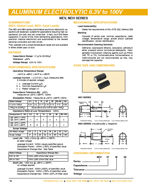
NEV, NEH SERIES32NTE Electronics, Inc. Voice (973) 748−5089 FAX (973) 748−6224 SUBMINIATURE(NEV: Radial Lead, NEH: Axial Leads)The NEV and NEH series subminiature aluminum electrolytic ca-pacitors are especially suitable for applications requiring high ca-pacitance, low cost, and very small size. In fact, you’ll find these capacitors in some of the most demanding applications, from precision medical electronics and automobiles to the newest personal computers and disk drives.They operate over a broad temperature range and are available in either blister pack or bulk.RATINGSCapacitance Range: 0.1f to 22,000f Tolerance: 20%Voltage Range: 6.3V to 100VPERFORMANCE SPECIFICATIONSOperating Temperature Range:−40C to +85C (−40F to +185F)Leakage Current: I 0.01CV + 3A (measured after3 minutes of applied voltage)I =Leakage Current (A)C =Nominal Capacitance (f)V =Rated Voltage (V)Capacitance Tolerance (M): 20%measured at +20C (+68F), 120HzDissipation Factor: measured at +20C (+68F),120HzRated Voltage 6.31016253550−801000.1f to 1000f 0.240.20.170.150.120.100.081000f to 22,000f Values above plus 0.02 for each 1000f Impedance Ratio at Low Temperature: 120HzComparison Z WV 6.31016253550−100Z @ −25C (−13F)/Z @ +20C (+68F)432222Z @ −40C (−40F)/Z @ +20C (+68F)864444Surge Voltage:DC Rated Voltage 6.3101625355063100Surge Voltage8132032446379125Load Life: 1000 12Hrs @ +85C (+185F),at rated voltageLeakage Current: Within values specified above Dissipation Factor: Within 150% of specified value Capacitance Change Max: See TableRated Voltage Capacitance Change Max6.3V to 16V Within 30% of the initial value 25V to 100VWithin 20% of the initial valueShelf Life: 1000 Hrs @ +85C (+185F),no voltage appliedLeakage Current: Within 200% of specified value Dissipation Factor: Within 150% of specified value Capacitance Change Max: Within 20% of initial valueMECHANICAL SPECIFICATIONSLead Solderability:Meets the requirements of MIL −STD 202, Method 208Marking:Consists of series type, nominal capacitance, rated voltage, temperature range, anode and/or cathode identification, vendor identification.Recommended Cleaning Solvents:Methanol, isopropanol ethanol, isobutanol, petroleum ether, propanol and/or commercial detergents. Halo-genated hydrocarbon cleaning agents such as Freon (MF, TF, or TC), trichloroethylene, trichloroethane, or methylchloride are not recommended as they may damage the capacitor.CASE SIZE AND DIMENSIONS:D’ Ø = D Ø + 0.5 MaxL’ = L + 1.0 Max at D Ø 8.0L’ = L + 2.0 Max at D Ø 10.0D’ Ø = D Ø + 0.5 Max L’ = L + 1.0 Max at D Ø 8.0L’ = L + 2.0 Max at D Ø 10.0NEV SERIESNEH SERIES(Insulating Bar = Negative)ORDERING INFORMATIONNEV47M50Series Capacitance Tolerance VoltageNEV Series (Radial Type) Dimensions: Diameter (D Ø) x Length (L): mmNEV Series (Radial Type) Mechanical Specifications: mmOutside Diameter (D Ø)5 6.381013161822 Lead Spacing (A)2 2.5 3.5557.57.510 Lead Diameter (d Ø)0.50.60.60.60.60.80.8 1.0*These dimensions are for reference only, please consult the factory for actual size.NTE Electronics, Inc. Voice (973) 748−5089 FAX (973) 748−6224 33NEH Series (Axial Type) Dimensions: Diameter (D Ø) x Length (L): mmNEH Series (Axial Type) Mechanical Specifications: mmOutside Diameter (D Ø)5 6.38101316182225 Lead Diameter (d Ø)0.60.60.60.60.80.80.80.80.8*These dimensions are for reference only, please consult the factory for actual size.34NTE Electronics, Inc. Voice (973) 748−5089 FAX (973) 748−6224 。
2N3906中文资料(nte)中文数据手册「EasyDatasheet - 矽搜」
VCE = 1V, I C = 1mA
40 − − 80 − −
2N3905 2N3906
VCE = 1V, I C = 10mA
50 − 150 100 − 300
2N3905 2N3906
VCE = 1V, I C = 50mA
30 − − 60 − −
2N3905 2N3906
VCE = 1V, I C = 100mA
芯片中文手册,看全文,戳
2N3905 & 2N3906 硅PNP晶体管
一般用途
TO92类型封装
绝对最大额定值:
集电极 - 发射极电压,V
CEO . . . . . . . . . . . . . . . . . . . . . . . . . . . . . . . . . . . . . . . . . . . . . . . . . . . . . . 40V
器件总功耗(T
C = +255C), PD . . . . . . . . . . . . . . . . . . . . . . . . . . . . . . . . . . . . . . . . . . . . 1.5W
减免上述255℃. . . . . . . . . . . . . . . . . . . . . . . . . . . . . . . . . . . . . . . . . . . . . . . . . . . . . . 12MW / 5C
减免上述255℃. . . . . . . . . . . . . . . . . . . . . . . . . . . . . . . . . . . . . . . 5.0MW / 5C
器件总功耗(T
CNT-90操作手册(1)
CNT-90操作手册基本控制对前后面板包括带菜单系统的用户界面的进一步描述会在该项说明之后介绍,这里简要介绍的目的是先给你熟悉以下仪器的界面。
INPUT A:A项输入打开菜单,从菜单上你能调整所有的A项设置,如阻抗衰减等等。
INPUT B:B项输入打开菜单,从菜单上你能调整所有的B项设置,如阻抗衰减等等。
SETTINGS:从该项菜单上你可以根据不同的测量功能及输出信道进行一些设置上的选择。
STANDBY LED备用LED:当频率计处于备用模式时该LED灯亮,表示电源仍然用在内部选择OCXO上(如果一个已经被安装)如果安装了铷振荡器则上电源LED持续是ON状态直到频率控制环路锁住(4-6分钟)。
STANDBY/ON备用/主用:触发几秒是电源开关,长按该按钮为备用模式。
将频率机打开并在关机时能储存设置。
MA TH/LIMIT:该菜单是用来选择一套公司用来修改测量结果,可以从键盘上输入3个恒值,还可以键入数值极限值用的统计报告和记录。
USER OPT用户选项:控制下列几项.1设置内存2界面3校验4自检5内部脉冲生成STA T/PLOT:输入已有的3种统计模式的一种,触发按键可切换模式V ALUE:输入通常的数值一个主参和若干辅参。
MEAS FUNC:菜单系列用来进行测量功能的选择,可以使用显示器下的快捷键来确认。
AUTO SET:自动调整输入触发电压到最佳值以选择测量功能光标控制。
CURSOR CONTROL:在显示器上进行内容切换,光标位置可以在四个方向上移动。
HOLD/RUN:在HOLD(点击一下)模式和RUN(连续按下)模式之见切换,如果采用HOLD 模式测量完成后自行停留在结果上。
RESTART重启:如果处于HOLD状态RESTART将重新开始一个新的测量。
EXIT/OK:确认菜单选项并退出菜单。
CANCEL:删除即不要确认选项的情况下退出。
SELECT:在不退出该菜单的情况下确认菜单选项。
连接器和指示器GRAPHIC DISPLAY(图形显示):300x97像素LED自带后备灯,输出测量结果的数值和图形形成显示,显示位于动态用户界面的中心,包括菜单系列指示器和信息栏。
- 1、下载文档前请自行甄别文档内容的完整性,平台不提供额外的编辑、内容补充、找答案等附加服务。
- 2、"仅部分预览"的文档,不可在线预览部分如存在完整性等问题,可反馈申请退款(可完整预览的文档不适用该条件!)。
- 3、如文档侵犯您的权益,请联系客服反馈,我们会尽快为您处理(人工客服工作时间:9:00-18:30)。
Features
Small size, light weight. Low coil power consumption, heavy contact load. Strong anti-shock and anti-vibration, high reliability, long life.
Suitable for automobile, machine, electronic equipment, air conditioner and household appliance applications.
PC board mounting.
Ordering Information
NT90 R H A S DC12V C B 0.9
1 2 3 4 5 6 7 8 91 Part number :NT90T 、NT90T 22 Terminal : R: without Pin 6;NIL: With Pin 6
3 Load :H:30A ;N:40A
4 Contact arrangement :1A:1A ;1B:1B ;1C:1C
5 Enclosure :S: Sealed type ;D: Dust cover ;
E: Covered ;O: Open type
6 Coil rated Voltage(V):AC:12,24,110,120,220
DC:3,5,6,9,12,15,18,24,48,1107 Contact material :C: Ag CdO ;S: Ag SnO 28 Resist heat class :B:130℃ F:155℃9 Coil power consumption :0.6:0.6W ;0.9:0.9W NIL:2VA Contact Data
Contact Arrangement
1A SPSTNO f 1B(SPSTNC)f 1C(SPDT(B-M))Contact Material
Ag CdO Ag SnO 2 Ag SnO 2 In 2O 3
Contact Rating (resistive)
NO : 30A/240VAC,14VDC; NC:20A/240VAC ;30A/14VDC NO :40A/250VAC,30VDC; NC:30A/250VAC,30VDC (0.9W)Motor load :2HP 250VAC ;1.5HP 250V Lamp load :TV-5
Max. Switching Power
1100W 7200VA Max. Switching Voltage
110VDC 250VAC Max. Switching Current:40A Contact Resistance or Voltage drop አ30m Item 3.12 of IEC255-7Electrical 105
Item 3.30 of IEC255-7Operation life Mechanical
107
Item 3.31 of IEC255-7
Coil Parameter
AC Coil Parameter
RATED VOLTAGE
VAC
DASH NUMBERS
RATED
Max
COIL RESISTANCE ±10%
PICK UP VOLTAGE VAC(max)(75%of rated voltage)RELEASE VOLTAGE VAC(min)(30%of rated voltage)
COIL POWER
Operate Time ms Release Time ms
012AC 1215.6279.0 3.6024AC 24
31.212018.0
7.2110AC 110143236082.533.0120AC 120156304090.036.0220AC
220
28613490165.066.0
2VA __
CAUTION : 1.The use of any coil voltage less than the rated coil voltage will compromise the operation of the relay.
2.Pickup and release voltage are for test purposes only and are not to be used as design criteria.
103
30.5×24.2×17 32.5×27.6×20.5 99312549.2 01311661.4
元器件交易网
003-9003 3.910
2.250.3005-9005 6.528
3.750.5006-90067.840
4.500.6009-900911.790 6.750.9012-900121
5.61609.00 1.2015-9001519.525010.25 1.5018-9001823.436013.50 1.8024-9002431.264018.00 2.4048-9004862.425603
6.00 4.8110-9001101431344582.5011.00.9
15
10
003-6003 3.915 2.250.3005-6005 6.542 3.750.5006-60067.860 4.500.6009-600911.7135 6.750.9012-6001215.62409.00 1.2015-6001519.537510.25 1.5018-6001823.454013.50 1.8024-6002431.296018.00 2.4048-6004862.4384036.00 4.8110-600
110
143
20167
82.50
11.0
0.6
15
10
CAUTION : 1.The use of any coil voltage less than the rated coil voltage will compromise the operation of the relay.
2.Pickup and release voltage are for test purposes only and are not to be used as design criteria.
Qualification inspection:
Perform the qualification test as specified in the table of IEC255-19-1 and minimum sample size 24.
Operation condition
Insulation Resistance 1000M min (at 500VDC)
Item 7 of IEC255-5Dielectric Strength Between contacts
Between contact and coil 50Hz 1500V 50Hz 2500V 4000V without Pin 6 Item 6 of IEC255-5
Item 6 of IEC255-5Shock resistance 200m/s 2 11ms
IEC68-2-27 Test Ea Vibration resistance 10~55Hz double amplitude 1.5mm IEC68-2-6 Test Fc Terminals strength 10N
IEC68-2-21 Test Ua1
Solderability
235 x 2 3x 0.5s IEC68-2-20 Test Ta method 1Ambient Temperature -55~100 -55~125 Relative Humidity 85% (at 40 )IEC68-2-3 Test Ca
Mass
27g Open type 30g
元器件交易网。