IXFT74N20中文资料
74HC20N中文资料

Fig.1 Pin configuration.
Fig.2 Logic symbol.
Fig.3 IEC logic symbol.
December 1990
3
元器件交易网
Philips Semiconductors
Dual 4-input NAND gate
Product specification
X
L
H
H
H
H
Notes
1. H = HIGH voltage level L = LOW voltage level X = don’t care
OUTPUT
nY
H H H H L
December 1990
4
元器件交易网
Philips Semiconductors
Dual 4-input NAND gate
28 90
115
nA, nB, nC, nD to nY
10 18
23
8 15
20
tTHL/ tTLH output transition time
19 75
95
7 15
19
6 13
16
TEST CONDITIONS
−40 to +125
UNIT
VCC (V)
WAVEFORMS
min. max.
135 ns 27 23
Note to HCT types The value of additional quiescent supply current (∆ICC) for a unit load of 1 is given in the family specifications. To determine ∆ICC per input, multiply this value by the unit load coefficient shown in the table below.
N74F04N资料

元器件交易网DIP14:plastic dual in-line package; 14 leads (300 mil)SOT27-1SO14:plastic small outline package; 14 leads; body width 3.9 mm SOT108-1NOTESDefinitionsShort-form specification — The data in a short-form specification is extracted from a full data sheet with the same type number and title. For detailed information see the relevant data sheet or data handbook.Limiting values definition — Limiting values given are in accordance with the Absolute Maximum Rating System (IEC 134). Stress above one or more of the limiting values may cause permanent damage to the device. These are stress ratings only and operation of the device at these or at any other conditions above those given in the Characteristics sections of the specification is not implied. Exposure to limiting values for extended periods may affect device reliability.Application information — Applications that are described herein for any of these products are for illustrative purposes only. Philips Semiconductors make no representation or warranty that such applications will be suitable for the specified use without further testing or modification.DisclaimersLife support — These products are not designed for use in life support appliances, devices or systems where malfunction of these products can reasonably be expected to result in personal injury. Philips Semiconductors customers using or selling these products for use in such applications do so at their own risk and agree to fully indemnify Philips Semiconductors for any damages resulting from such application.Right to make changes — Philips Semiconductors reserves the right to make changes, without notice, in the products, including circuits, standard cells, and/or software, described or contained herein in order to improve design and/or performance. Philips Semiconductors assumes no responsibility or liability for the use of any of these products, conveys no license or title under any patent, copyright, or mask work right to these products, and makes no representations or warranties that these products are free from patent, copyright, or mask work right infringement, unless otherwise specified.Philips Semiconductors811 East Arques AvenueP.O. Box 3409Sunnyvale, California 94088–3409Telephone 800-234-7381© Copyright Philips Electronics North America Corporation 1998All rights reserved. Printed in U.S.A.print code Date of release: 10-98。
IXFN80N50中文资料

rated
? Low package inductance ? Fast intrinsicRectifier
0.001
10 -4
10 -3
10 -2
10 -1
10 0
10 1
Pulse Width - Seconds
IXYS reserves the right to change limits, test conditions, and dimensions.
IXYS MOSFETS and IGBTs are covered by one or more ofthe following U.S. patents:
10000
pF -
e
acitanc
1000
ap
C
Ciss Coss
f = 100kHz
Crss
100 0
5 10 15 20 25 30 35 40 VDS - Volts
Figure 9. Forward Voltage Drop of the Intrinsic Diode
100
V GS = 0V
? Easy to mount ? Space savings ? High power density
? 2002 IXYS All rights reserved
98538C (02/02)
IXFN 75N50 IXFN 80N50
Symbol
gfs Ciss Coss Crss td(on) tr t
ATR2740_07资料

Features•Highly Integrated Digital Device for DAB Receivers (Eureka147)•Utilizes the ARM7TDMI® Core–High-performance 32-bit RISC Architecture–High-density 16-bit Instruction Set–Embedded ICE (In-Circuit Emulation)•Utilizes TeakDSPCore™–16-bit Fixed-point Digital Signal Processing Core•HDAB OFDM Channel Demodulator and Decoder–Fully Integrated, Supports all DAB Functions andModes–Full Data Rate of 1.8Mbit Can Be Decoded–Automatic Mode Detection (AMD)–Digital AFC (Frequency Tolerance < 0.5Hz for Mode I)–Digital AGC with a Wide Gain Control Range–Demodulation and Decoding of up to 64 UEP/EEP Sub-channels•Audio Source Decoder (ASD) and Data Decoder (DD)–On-chip De-interleaver Memory for Full 1.8Mbit/s Decoding Data Rate–PAD Extraction–Two Independent Data Packet Mode Decoder•Integrated High-density SRAM Supporting Time and Frequency De-interleaving •10Msps High-speed Low-power Pipelined ADC–Supports Wide IF Range of 2.048MHz to 50MHz–Complex Bandpass Filtering–Optional SAW Filter Equalization•ARM7TDMI Core User Software Extension–Audio Player MP3 Support•Large Variety of Interfaces–I2S/SPDIF, SFCO, SSO, RDI, RS-232, USART–USB V1.1 Full Speed–Two USARTs–CAN 2.0A and 2.0B•Master/Slave SPI Interface–Two Dedicated Peripheral Data Controller (PDC) Channels–8- to 16-bit Programmable Data Length–Four External Slave Chip Selects•Programmable Watchdog Timer•Power Management Controller (PMC)–CPU and Peripherals Can Be De-activated Individually–Simple But Comfortable Gearing and Clocking Unit•32 User Programmable I/O Lines (PIO)•Low-power Consumption for Portable Applications (3.3V and 1.8V)•Robust LQFP128 Package, BGA121 Package•Very Low External Component Count24816ES–DAB–01/07ATR2740[Preliminary]1.DescriptionThe ATR2740 is a fully integrated processing unit which covers all DAB- (Eureka 147,ETS 300401) related digital tasks like DAB OFDM demodulation and decoding, audio source decoding, data decoding, as well as time and frequency synchronization.The device consists of a high-performance 32-bit RISC ARM7TDMI core, an additional TeakDSPCore, embedded memories, an analog-to-digital converter (ADC), as well as a DAB channel demodulator and decoder IP, and two independent audio source decoder engines. A large variety of interfaces, including USB, SPI, USART and RDI, are provided.The ATR2740 baseband processor is controlled by a standard ARM7TDMI core, which is a very well-known controller. This allows the designers to work with standard tools, which results in reduced development costs and very fast time to market.The ARM7TDMI core is designed to perform the DAB receiver tasks, MMI and further user soft-ware extensions such as MP3 decoding or data decoding.The ATR2740 is manufactured using Atmel’s high-density CMOS technology. By combining all functions on one SoC (System-on-Chip), including a wide range of peripheral functions on a monolithic chip, the ATR2740 provides a highly flexible and cost-effective solution for DAB applications.The advanced Atmel technology and the architecture of the ATR2740 enable maximum perfor-mance at a very low current consumption.The wide flexibility offered by the ATR2740 is due to the large variety of interfaces supported.For control functions, UART, USB, and SPI are available. As data interfaces, an SSO, SFCO,US Band RDI, as well as two audio outputs (either I 2S or SPDIF), are available.Due to the high integration of the device, the external component count is as low as only two external parts; a simple crystal and a 16-MB flash memory are required to run the full DAB func-tion. All RAM, such as interleaving or program memory, as well as the ADC are incorporated into the device. The part works perfectly together with Atmel’s DAB front-end parts.The processing power available with the ATR2740 is sufficient to enable the part to decode the full DAB data rate of 1.8Mbits. In addition, there is still unused processing power available on the ARM7TDMI controller for customer software. It is easy to run a complete MP3 player without the need to add extra hardware to the device.A complete set of tools for hardware and software, including documentation that allows easy design-in and a fast time to market, is available on request.34816ES–DAB–01/07ATR2740[Preliminary]Figure 1-1.Block Diagram44816ES–DAB–01/07ATR2740[Preliminary]Electrostatic sensitive device.Observe precautions for handling.2.Absolute Maximum RatingsStresses beyond those listed under “Absolute Maximum Ratings” may cause permanent damage to the device. This is a stress rating only and functional operation of the device at these or any other conditions beyond those indicated in the operational sections of this specification is not implied. Exposure to absolute maximum rating conditions for extended periods may affect device reliability.ParametersSymbolMin.Max.Unit Operating free air temperature range for LQFP128–40+85°C Operating free air temperature range for BGA121–10+70°C Storage temperature T Stg –60+150°C DC supply voltage VDD18–0.3+1.95V VDD33–0.3+3.6V AVDD –0.3+3.6V DC input voltage –0.3+1.95VNotes:1.The part may not survive if all maximums are applied simultaneously.3.DC Electrical CharacteristicsT est conditions (if not otherwise specified): V CC = +1.8V , T amb = +25°C No.Parameters Test ConditionsPinSymbol Min.Typ.Max.Unit Type*1.1DC supply voltage VDD18 1.65 1.81.95V 1.2Low-level input voltage VDD18 = 1.65 to 1.95V V IL –0.3+0.3 × VDD18V 1.3High-level input voltageVDD18 = 1.65 to 1.95V V IH +0.7 × VDD18VDD18 + 0.3V 1.4Low-level output voltageI OL = 0.3mA VDD18 = 1.65V V OL 0.1V 1.5High-level output voltageI OH = 0.3 mA VDD18 = 1.65V V OHVDD18 – 0.1V 1.12Crystal oscillator frequency 24.576MHz 1.13Clock duty cycle 4060%1.15USB DC supply voltageFull speedVDD3333.33.6V 1.16USB input low level VILUSB 0.8V 1.17USB input high level VIHUSB 2.0V 1.18USB differential input sensitivityVDIUSB 0.2V 1.19USB differential input common mode rangeVCMUSB0.82.5V*) T ype means: A = 100% tested, B = 100% correlation tested, C = Characterized on samples, D = Design parameter54816ES–DAB–01/07ATR2740[Preliminary]1.20USB output low level VOLUSB 0.00.3V 1.21USB output high level VOHUSB2.83.6V 1.22Transition rise time Full speed TFR 420ns 1.23Transition fall time Full speed TFE 420ns 1.24USB crystal oscillator frequencyFUSB489MHz 1.25USB clock duty cycle 4060%1.26JTAG TCK frequencyFTCK0.0233MHz3.DC Electrical Characteristics (Continued)T est conditions (if not otherwise specified): V CC = +1.8V , T amb = +25°C No.Parameters Test ConditionsPinSymbol Min.Typ.Max.Unit Type**) T ype means: A = 100% tested, B = 100% correlation tested, C = Characterized on samples, D = Design parameter4.Electrical Characteristics on ADC/IF InputT est conditions (if not otherwise specified): V CC = +3.3V , T amb = +25°C No.Parameters Test ConditionsPinSymbol Min.Typ.Max.Unit Type*2.1ADC DC supply voltageAVDD 3 3.33.6V 2.2IF frequency rangeFIF2.04850MHz*) T ype means: A = 100% tested, B = 100% correlation tested, C = Characterized on samples, D = Design parameter5.DC Power ConsumptionT est conditions (if not otherwise specified): V CC = +1.8V , T amb = +25°C Mode ConditionsTyp.Max.Unit Core Power ConsumptionDAB fullDecode of all MSC’s and 1 audio sub-channel80mA64816ES–DAB–01/07ATR2740[Preliminary]7.Package Information LQFP1286.Ordering InformationExtended Type Number Package RemarksA TR2740-RQHH LQFP12816 mm × 16 mm, 0.40 mm pitch, lead free A TR2740-7GHGBGA12110 mm × 10 mm, 0.80 mm pitch, lead free74816ES–DAB–01/07ATR2740[Preliminary]8.Package Information BGA121Disclaimer: The information in this document is provided in connection with Atmel products. No license, express or implied, by estoppel or otherwise,to any intellectual property right is granted by this document or in connection with the sale of Atmel products. EXCEPT AS SET FORTH IN ATMEL ’S TERMS AND CONDI-TIONS OF SALE LOCATED ON ATMEL ’S WEB SITE, ATMEL ASSUMES NO LIABILITY WHATSOEVER AND DISCLAIMS ANY EXPRESS, IMPLIED OR STATUTORY WARRANTY RELATING TO ITS PRODUCTS INCLUDING, BUT NOT LIMITED TO, THE IMPLIED WARRANTY OF MERCHANTABILITY, FITNESS FOR A PARTICULAR PURPOSE, OR NON-INFRINGEMENT. IN NO EVENT SHALL ATMEL BE LIABLE FOR ANY DIRECT, INDIRECT, CONSEQUENTIAL, PUNITIVE, SPECIAL OR INCIDEN-TAL DAMAGES (INCLUDING, WITHOUT LIMITATION, DAMAGES FOR LOSS OF PROFITS, BUSINESS INTERRUPTION, OR LOSS OF INFORMATION) ARISING OUT OF THE USE OR INABILITY TO USE THIS DOCUMENT, EVEN IF ATMEL HAS BEEN ADVISED OF THE POSSIBILITY OF SUCH DAMAGES. Atmel makes no representations or warranties with respect to the accuracy or completeness of the contents of this document and reserves the right to make changes to specifications and product descriptions at any time without notice. Atmel does not make any commitment to update the information contained herein. Unless specifically provided otherwise, Atmel products are not suitable for, and shall not be used in, automotive applications. Atmel’s products are not intended, authorized, or warranted for use as components in applications intended to support or sustain life.Atmel CorporationAtmel Operations2325 Orchard Parkway San Jose, CA 95131, USA Tel: 1(408) 441-0311Fax: 1(408) 487-2600Regional HeadquartersEuropeAtmel SarlRoute des Arsenaux 41Case Postale 80CH-1705 Fribourg SwitzerlandTel: (41) 26-426-5555Fax: (41) 26-426-5500AsiaRoom 1219Chinachem Golden Plaza 77 Mody Road Tsimshatsui East Kowloon Hong KongTel: (852) 2721-9778Fax: (852) 2722-1369Japan9F, Tonetsu Shinkawa Bldg.1-24-8 ShinkawaChuo-ku, Tokyo 104-0033JapanTel: (81) 3-3523-3551Fax: (81) 3-3523-7581Memory2325 Orchard Parkway San Jose, CA 95131, USA Tel: 1(408) 441-0311Fax: 1(408) 436-4314Microcontrollers2325 Orchard Parkway San Jose, CA 95131, USA Tel: 1(408) 441-0311Fax: 1(408) 436-4314La Chantrerie BP 7060244306 Nantes Cedex 3, France Tel: (33) 2-40-18-18-18Fax: (33) 2-40-18-19-60ASIC/ASSP/Smart CardsZone Industrielle13106 Rousset Cedex, France Tel: (33) 4-42-53-60-00Fax: (33) 4-42-53-60-011150 East Cheyenne Mtn. Blvd.Colorado Springs, CO 80906, USA Tel: 1(719) 576-3300Fax: 1(719) 540-1759Scottish Enterprise Technology Park Maxwell BuildingEast Kilbride G75 0QR, Scotland Tel: (44) 1355-803-000Fax: (44) 1355-242-743RF/AutomotiveTheresienstrasse 2Postfach 353574025 Heilbronn, Germany Tel: (49) 71-31-67-0Fax: (49) 71-31-67-23401150 East Cheyenne Mtn. Blvd.Colorado Springs, CO 80906, USA Tel: 1(719) 576-3300Fax: 1(719) 540-1759BiometricsAvenue de Rochepleine BP 12338521 Saint-Egreve Cedex, France Tel: (33) 4-76-58-47-50Fax: (33) 4-76-58-47-60Literature Requests/literature4816ES–DAB–01/07© Atmel Corporation 2007. All rights reserved. Atmel ®, logo and combinations thereof, Everywhere You Are ® and others, are registered trade-marks or trademarks of Atmel Corporation or its subsidiaries. ARM7TDMI ® is a registered trademark of ARM Ltd. TeakDSPCore ™ is a trademark of DSP Group Inc. Other terms and product names may be trademarks of others.。
74HC20中文资料

AC CHARACTERISTICS FOR 74HC GND = 0 V; tr = tf = 6 ns; CL = 50 pF
Tamb (°C)
SYMBOL
PARAMETER
74HC
+25
−40 to +85
min. typ. max. min. max.
tPHL/ tPLH propagation delay
74HC/HCT20
Fig.4 Functional diagram. Fig.6 HCT logic diagram (one gate).
Fig.5 HC logic diagram (one gate).
FUNCTION TABLE
INPUTS
nA nB nC nD
L
X
X
X
X
L
X
X
X
X
L
X
X
X
Philips Semiconductors
Dual 4-input NAND gate
PIN DESCRIPTION
PIN NO. 1, 9 2, 10 3, 11 4, 12 5, 13 6, 8 7 14
EPM1270T144I5N中文资料(Altera)中文数据手册「EasyDatasheet - 矽搜」

器
BGA(1)
EPM240
—
EPM240G
EPM570
—
EPM570G
EPM1270
—
EPM1270G
EPM2210
—
EPM2210G
EPM240Z
54
EPM570Z
—
注意 表 1-3: (1)包装只有无铅版本.
100-Pin Micro FineLine BGA(1)
80
76
—
—
80 76
100-Pin FineLine
每一个速度等级和密度范围内数字,指是
特点
在本章
MAX II器件手册.
表1-2 显示MAX II器件速度等级产品.
DC和开关
表 1-2. MAX II速度等级
速度等级
器
EPM240 EPM240G EPM570 EPM570G EPM1270 EPM1270G EPM2210 EPM2210G EPM240Z EPM570Z
芯片中文手册,看全文,戳
1.简介
MII51001-1.9
简介
马克斯 II系列瞬时上电,非易失性CPLD产品是基于0.18微米, 6层金属闪光过程中,用从240到2210逻辑单元(LE)(128〜2210当量宏小区)和8千位非 易失性存储密度. MAX II器件提供高I / O数量,快速性能,可靠配件与其他 CPLD架构.拥有多电压核心,用户闪存(UFM)模块,以及增强在系统编程( ISP),MAX II器件设计,以降低成本和功耗,同时提供可编程解决方案应用 ,如总线桥接,I / O扩展,电源-on复位(POR)和顺序控制和设备配置控 制.
3.3 V, 2.5 V
1.5 V, 1.8 V, 2.5 V, 3.3 V
74LS00N中文资料

© 2000 Fairchild Semiconductor Corporation DS006439August 1986Revised March 2000DM74LS00 Quad 2-Input NAND GateDM74LS00Quad 2-Input NAND GateGeneral DescriptionThis device contains four independent gates each of which performs the logic NAND function.Ordering Code:Devices also available in T ape and Reel. Specify by appending the suffix letter “X” to the ordering code.Connection Diagram Function TableY = ABH = HIGH Logic Level L = LOW Logic LevelOrder Number Package NumberPackage DescriptionDM74LS00M M14A 14-Lead Small Outline Integrated Circuit (SOIC), JEDEC MS-120, 0.150 Narrow DM74LS00SJ M14D 14-Lead Small Outline Package (SOP), EIAJ TYPE II, 5.3mm Wide DM74LS00NN14A14-Lead Plastic Dual-In-Line Package (PDIP), JEDEC MS-001, 0.300 WideInputs OutputA B Y L L H L H H H L H HHL 2D M 74L S 00Absolute Maximum Ratings (Note 1)Note 1: The “Absolute Maximum Ratings” are those values beyond which the safety of the device cannot be guaranteed. The device should not be operated at these limits. The parametric values defined in the Electrical Characteristics tables are not guaranteed at the absolute maximum ratings.The “Recommended Operating Conditions” table will define the conditions for actual device operation.Recommended Operating ConditionsElectrical Characteristicsover recommended operating free air temperature range (unless otherwise noted)Note 2: All typicals are at V CC = 5V, T A = 25°C.Note 3: Not more than one output should be shorted at a time, and the duration should not exceed one second.Switching Characteristicsat V CC = 5V and T A = 25°CSupply Voltage 7V Input Voltage7VOperating Free Air Temperature Range 0°C to +70°C Storage Temperature Range−65°C to +150°CSymbol ParameterMin Nom Max Units V CC Supply Voltage4.7555.25V V IH HIGH Level Input Voltage 2V V IL LOW Level Input Voltage 0.8V I OH HIGH Level Output Current −0.4mA I OL LOW Level Output Current 8mA T AFree Air Operating Temperature70°CSymbol ParameterConditionsMinTyp Max Units (Note 2)V I Input Clamp Voltage V CC = Min, I I = −18 mA −1.5V V OH HIGH Level V CC = Min, I OH = Max, 2.73.4VOutput Voltage V IL = Max V OLLOW Level V CC = Min, I OL = Max,0.350.5Output VoltageV IH = MinVI OL = 4 mA, V CC = Min 0.250.4I I Input Current @ Max Input Voltage V CC = Max, V I = 7V 0.1mA I IH HIGH Level Input Current V CC = Max, V I = 2.7V 20µA I IL LOW Level Input Current V CC = Max, V I = 0.4V −0.36mA I OS Short Circuit Output Current V CC = Max (Note 3)−20−100mA I CCH Supply Current with Outputs HIGH V CC = Max 0.8 1.6mA I CCLSupply Current with Outputs LOWV CC = Max2.44.4mAR L = 2 k ΩSymbol ParameterC L = 15 pF C L = 50 pF UnitsMin Max Min Max t PLH Propagation Delay Time 310415ns LOW-to-HIGH Level Output t PHLPropagation Delay Time 310415ns HIGH-to-LOW Level OutputDM74LS00Physical Dimensions inches (millimeters) unless otherwise noted14-Lead Small Outline Integrated Circuit (SOIC), JEDEC MS-120, 0.150 NarrowPackage Number M14A 4D M 74L S 00Physical Dimensionsinches (millimeters) unless otherwise noted (Continued)14-Lead Small Outline Package (SOP), EIAJ TYPE II, 5.3mm WidePackage Number M14D5DM74LS00 Quad 2-Input NAND GatePhysical Dimensions inches (millimeters) unless otherwise noted (Continued)14-Lead Plastic Dual-In-Line Package (PDIP), JEDEC MS-001, 0.300 WidePackage Number N14AFairchild does not assume any responsibility for use of any circuitry described, no circuit patent licenses are implied and Fairchild reserves the right at any time without notice to change said circuitry and specifications.LIFE SUPPORT POLICYFAIRCHILD’S PRODUCTS ARE NOT AUTHORIZED FOR USE AS CRITICAL COMPONENTS IN LIFE SUPPORT DEVICES OR SYSTEMS WITHOUT THE EXPRESS WRITTEN APPROVAL OF THE PRESIDENT OF FAIRCHILD SEMICONDUCTOR CORPORATION. As used herein:1.Life support devices or systems are devices or systems which, (a) are intended for surgical implant into the body, or (b) support or sustain life, and (c) whose failure to perform when properly used in accordance with instructions for use provided in the labeling, can be rea-sonably expected to result in a significant injury to the user.2. A critical component in any component of a life support device or system whose failure to perform can be rea-sonably expected to cause the failure of the life support device or system, or to affect its safety or effectiveness.。
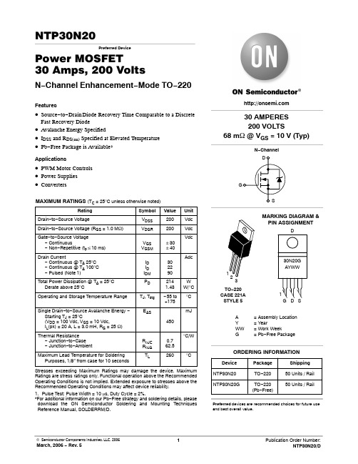
NTP30N20中文资料
IDSS
mAdc
−
−
5.0
−
−
125
IGSS
−
−
± 100 nAdc
VGS(th)
Vdc
2.0
2.9
4.0
−
−8.9
−
mV/°C
Static Drain−to−Source On−State Resistance (VGS = 10 Vdc, ID = 15 Adc) (VGS = 10 Vdc, ID = 10 Adc) (VGS = 10 Vdc, ID = 15 Adc, TJ = 175°C)
VSD
trr ta tb QRR
−
75
100
nC
−
48
−
−
20
−
−
16
−
−
32
−
−
0.91
1.1
Vdc
−
0.80
−
−
230
−
ns
−
140
−
−
85
−
−
1.85
−
mC
2
ID, DRAIN CURRENT (AMPS)
RDS(on), DRAIN−TO−SOURCE RESISTANCE (W)
Drain Current − Continuous @ TA 25°C − Continuous @ TA 100°C − Pulsed (Note 1)
Total Power Dissipation @ TA = 25°C Derate above 25°C
VDSS VDGR
VGS VGSM
ID ID IDM PD
- 1、下载文档前请自行甄别文档内容的完整性,平台不提供额外的编辑、内容补充、找答案等附加服务。
- 2、"仅部分预览"的文档,不可在线预览部分如存在完整性等问题,可反馈申请退款(可完整预览的文档不适用该条件!)。
- 3、如文档侵犯您的权益,请联系客服反馈,我们会尽快为您处理(人工客服工作时间:9:00-18:30)。
© 2000 IXYS All rights reserved
SymbolTest ConditionsMaximum Ratings
VDSSTJ= 25°C to 150°C200V
VDGRTJ= 25°C to 150°C; RGS = 1 MW200V
VGSContinuous±20V
VGSMTransient±30V
ID25TC= 25°C68N2068A
74N2074A
IDMTC= 25°C, pulse width limited by TJM68N20272A
74N20296A
IARTC= 25°C68N2068A
74N2074A
EARTC= 25°C45mJ
dv/dtIS£ IDM, di/dt £ 100 A/ms, VDD £ VDSS,5V/ns
TJ £ 150°C, RG = 2 W
PDTC= 25°C360W
TJ-55 ... +150°C
T
JM
150°C
Tstg-55 ... +150°C
TL1.6 mm (0.062 in.) from case for 10 s300°C
MdMounting torque1.13/10Nm/lb.in.
Weight 6g
SymbolTest ConditionsCharacteristic Values
(TJ = 25°C, unless otherwise specified)
min.typ.max.
VDSSVGS= 0 V, ID = 1 mA200V
V
GS(th)VDS= VGS, ID
= 4 mA24V
IGSSVGS= ±20 VDC, VDS = 0±100nA
IDSSVDS= 0.8 VDSSTJ = 25°C200mA
VGS= 0 VTJ = 125°C1mA
RDS(on) VGS= 10 V, ID = 0.5 ID2574N2030mW
68N2035mW
Pulse test, t £ 300 ms, duty cycle d £ 2 %
HiPerFET
TM
Power MOSFETs
N-Channel Enhancement Mode
High dv/dt, Low trr, HDMOSTM Family
TO-247 AD (IXFH)
Features
International standard packages
Low RDS (on) HDMOSTM process
Rugged polysilicon gate cell structure
Unclamped Inductive Switching (UIS)
rated
Low package inductance
-easy to drive and to protect
Fast intrinsic Rectifier
Applications
DC-DC converters
Synchronous rectification
Battery chargers
Switched-mode and resonant-mode
power supplies
DC choppers
AC motor control
Temperature and lighting controls
Low voltage relays
Advantages
Easy to mount with 1 screw (TO-247)
(isolated mounting screw hole)
High power surface package
High power density
G = Gate,D = Drain,
S = Source,TAB = Drain
97522C (8/00)
(TAB)
VDSSID25R
DS(on)
IXFH/IXFT 68N20
200 V68 A35 mW
IXFH/IXFT 74N20
200 V74 A30 mW
trr £ 200 ns
TO-268 (D3) ( IXFT)
(TAB)
G
S
元器件交易网www.cecb2b.com
IXYS MOSFETS and IGBTs are covered by one or more of the following U.S. patents:4,835,5924,881,1065,017,5085,049,9615,187,1175,486,715
4,850,0724,931,8445,034,7965,063,3075,237,4815,381,025
IXYS reserves the right to change limits, test conditions, and dimensions.
SymbolTest ConditionsCharacteristic Values
(TJ = 25°C, unless otherwise specified)Min. Typ.Max.
gfsVDS= 10 V; ID = 0.5 ID25, pulse test3545S
C
iss
5400pF
CossVGS= 0 V, VDS = 25 V, f = 1 MHz1160pF
Crss560pF
td(on)40ns
trVGS= 10 V, VDS = 0.5 VDSS, ID = 0.5 ID2555ns
td(off)RG= 2 W (External)120ns
tf26ns
Qg(on)280nC
QgsVGS= 10 V, VDS = 0.5 VDSS, ID = 0.5 ID2539nC
Qgd135nC
RthJC0.35K/W
R
thCK
(TO-247 Package)0.25K/W
IXFH68N20 & IXFH74N80 characteristic curves can be found in the IXFK72N20/
IXFK80N20 data sheet.
Source-Drain DiodeCharacteristic Values
(TJ = 25°C, unless otherwise specified)
SymbolTest ConditionsMin.Typ. Max.
ISVGS= 0 V68N2068A
74N2074A
I
SM
Repetitive;68N20272A
pulse width limited by TJM74N20296A
VSDIF = IS, VGS = 0 V,1.5V
Pulse test, t £ 300 ms, duty cycle d £ 2 %
trr200ns
QRM0.85mC
8A
I
RM
IF = 25A
-di/dt = 100 A/ms,
VR = 100 V
TO-247 AD (IXFH) Outline
Dim.MillimeterInches
Min.Max.Min.Max.
A4.75.3.185.209
A
1
2.22.54.087.102
A22.22.6.059.098
b1.01.4.040.055
b
1
1.652.13.065.084
b22.873.12.113.123
C.4.8.016.031
D20.8021.46.819.845
E15.7516.26.610.640
e5.205.720.2050.225
L19.8120.32.780.800
L14.50.177
ÆP3.553.65.140.144
Q5.896.400.2320.252
R4.325.49.170.216
S6.15BSC242BSC
Terminals:
1 - Gate
2 - Drain
3 - Source
Tab - Drain
1 2 3
TO-268 Outline
IXFH 68N20IXFH 74N20
IXFT 68N20IXFT 74N20
Min Recommended Footprint
元器件交易网www.cecb2b.com