2SD2121 PDF规格书
PI2121-EVAL1;中文规格书,Datasheet资料

IntroductionThe PI2121-EVAL1 allows the user to test the basic principle and operational characteristics of an Active ORing function in a redundant power architecture, while also experiencing the benefits and value of the PI2121 solution versus conventional Active ORing solutions. The PI2121-EVAL1 evaluation board is configured to receive two independent power source inputs,per a typical redundant power architecture, through two Active ORing channels that are combined to form aredundant power output. Each channel is capable of up to 24A, and is suitable for redundant bus voltages up to 5 V. For high current Active ORing, above 24 A, the two channels provided on the evaluation board can be paralleled in amaster/slave configuration and OR'd with a second evaluation board.The PI2121-EVAL1 evaluation board is designed withoptimized PCB layout and component placement to represent a realistic high density final design for an embedded Active ORing solution for ≤5V bus applications requiring up to 24 A.This evaluation board is intended as an easy and simple way to test the electrical and thermal performance of the PI2121 Full-Function Active ORing solution.Both dynamic and steady state testing of the PI2121 can be completed on the PI2121-EVAL1 evaluation board, in addition to using the key features of the product. Dynamic testing can be completed under a variety of system level fault conditions to check for response time to faults.This document provides basic instructions for initial start-up and configuration of the evaluation board. Furtherinformation on the functionality of the PI2121 can be found in the PI2121 product data sheet.PI2121-EVAL1Cool-ORing ™ SeriesPI2121-EVAL1 Full-Function Active ORingEvaluation Board User Guide®PI2121-EVAL1 Evaluation Board featuring the Cool-ORing PI2121 Full-Function Active ORing Solution.Cool-ORing™ SeriesThe PI2121-EVAL1 Evaluation Board is intended to acquaint the user with the benefits and features of the Cool-ORing TM PI2121full function Active ORing solution. It is not designed to be installed in end-use equipment.Please read this document before setting up the PI2121-EVAL1Evaluation Board and refer to the PI2121 product data sheet for device specifications, functional description and characteristics.During operation, the power devices and surrounding structures can be operated safely at high temperatures.•Remove power and use caution when connecting and disconnecting test probes and interface lines to avoid inadvertent short circuits and contact with hot surfaces.•When testing electronic products always use approved safety glasses. Follow good laboratory practice and procedures.The Cool-ORing PI2121 is a complete full-function Active ORing solution with a high-speed ORing MOSFET controller and a very low on-state resistance MOSFET designed for use in redundant power system architectures. The PI2121 Cool-ORing solution is offered in an extremely small, thermally enhanced 5 mm x 7 mm LGA package and can be used in low voltage (≤5 Vbus) high side Active ORing applications. ThePI2121 enables extremely low power loss with fast dynamic response to fault conditions, critical for high availability systems. A master/ slave feature allows the paralleling ofPI2121 solutions for high current Active ORing requirements. The PI2121, with its 1.5 mΩinternal MOSFET provides very high efficiency and low power loss during steady state operation, while achieving high-speed turn-off of the internal MOSFET during input power source fault conditions that cause reverse current flow. The PI2121 provides an active low fault flag output to the system during excessive forward current, light load, reverse current, over-voltage,under-voltage, and over-temperature fault conditions.A temperature sensing function indicates a fault if the maximum junction temperature exceeds 160°C. Theunder-voltage and over-voltage thresholds are programmable via an external resistor divider.Figure 1 shows a photo of the PI2121-EVAL1 evaluation board, with two PI2121 used to form the two Active ORing channels. The board is built with two identical Active ORing circuits with options and features that enable the user to fullyexplore the capabilities of the PI2121 Cool-ORing solution. Figure 1 –PI2121-EVAL1 Evaluation Board (1.8" x 1.8")Terminals RatingVin1, Vin28V / 24 AVaux1, Vaux2, (R7 = R14 = 10 Ω)-0.3 to 17.3 V / 40 mAsee Vaux sectionSL-0.3 to 8.0 V / 10 mAFT-0.3 to 17.3 V / 10 mATerminal DescriptionVin1Power Source Input #1or bus input designed to accommodate up to 24 A continuous current.Vaux1Auxiliary Input Voltage #1to supply PI2121 (SiP1) VC power. Vaux1 should be equal to Vin1 plus5 V or higher. See details in Auxiliary Power Supply (Vaux) section of the PI2121 data sheet.Rtn1Vaux1 Return Connection: Connected to Ground planeGnd Vin & Vout Return Connection:Three Gnd connections are available and are connected to a commonpoint, the Ground plane. Input supplies Vin1 & Vin2 and the output load at Vout should all beconnected to their respective local Gnd connection.SL1PI2121 (SiP1) Slave Input-Output Pin:For monitoring SiP1 slave pin. When SiP1 is configured as theMaster, this pin functions as an output that drives slaved PI2121 devices. When SiP1 is configured inSlave mode, SL1 serves as an input.SL2PI2121 (SiP2) Slave Input-Output Pin:For monitoring SiP2 slave pin. When SiP2 is configured as theMaster, this pin functions as an output that drives slaved PI2121 devices. When SiP2 is configured inSlave mode, SL2 serves as an input.Vin2Power Source Input #2or bus input designed to accommodate up to 24 A continuous current.Vaux2Auxiliary Input Voltage #2to supply PI2121 (SiP2) VC power. Vaux2 should be equal to Vin2 plus 5 V or higher.See details in Auxiliary Power Supply (Vaux) section of the PI2121 data sheet.Rtn2Vaux2 Return Connection: Connected to Ground planeFT1PI2121 (SiP1) Fault Pin:Monitors SiP1 fault conditionsFT2PI2121 (SiP2) Fault Pin: Monitors SiP2 fault conditionsVout Output: SiP1 and SiP2 D pins connection, connect to the load high side.Table 1 –PI2121-EVAL1 Evaluation Board terminals descriptionCool-ORing TM PI2121 Product DescriptionJumper DescriptionJ1, J3BK Jumpers: Connect jumper across M for master mode and across S for slave mode. Remove jumper to adjust reverse fault blanking time using Rbk. Rbk is R6 for SiP1 and R13 for SiP2 shown in the schematic, Figure 2.J2Slave Jumper: Remove the jumper unless one of the PI2121 is configured in slave mode.Table 2 –PI2121-EVAL1 Evaluation Board jumpers descriptionFigure 2 –PI2121-EVAL1 Evaluation Board schematic.Item QTY Reference Designator Value Description Footprint Manufacturer 12C1, C2 1 µF Capacitor, MLCC X5R, 06031 µF,16 V21C322 µF Capacitor, MLCC X7R,121022 µF, 25 V34C4, C5, C6, C7Not installed120642D1, D2LED, Super Red THIN 0603Lite-On, Inc.,58FT1, FT2, Rtn1, Rtn2, Turret Test point TURRET-1528Keystone SL1, SL2, Vaux1, Vaux2Electronics67Gnd1, Gnd2, Gnd3, Gnd4,Turret Test point TURRET-1502Keystone Vin1, Vin2, Vout1, Vout2Electronics 72J1, J3Header Pins 0.1" pitch 2 x 3mm81J2Header Pins 0.1" pitch 2 x 2mm92R1, R88.45 KΩResistor, 8.45 KΩ, 1%0603102R2, R913.3 KΩResistor,13.3 KΩ,1%0603114R3, R4, R10, R11 2.00 KΩResistor, 2.00 KΩ,1%0603122R5, R12 4.99 KΩResistor, 4.99 KΩ,1%0603132R6, R13Not Installed0603142R7, R1410Resistor, 10, 5%0603152SiP1, SiP2PI2121Picor Full-Function 24 A 5x7mm;17 pins PICORCool-ORing SolutionTable 3 –PI2121-EVAL1 Evaluation Board bill of materialsInitial Test Set UpTo test the PI2121-EVAL1 evaluation board it is necessary to configure the jumpers (J1, J2 and J3) first based on the required board configuration.Failure to configure the jumpers prior to the testing may result in improper circuit behavior.Baseline Test Procedure (Refer to Figure 3)1.0 Recommended Equipment1.1Two DC power supplies - 0-10 V; 25 A.1.2DC power supply 12 V; 100 mA.1.3DC electronic load - 50 A minimum.1.4Digital Multimeter 1.5Oscilloscope.1.6Appropriately sized interconnect cables.1.7Safety glasses.1.8PI2121 Product Data sheet.Figure 3 –Layout configuration for a typical redundant power application, using PI2121 with both solutions configured in Master Mode.Reference Designator Value Functional Description C1, C21µF VC Bypass Capacitor C322µF Output (Load) CapacitorC4, C5, C6, C7Not installedSnubber to reduce voltage ringing when the device turns off D1, D2LED To indicate a fault exist when it is onJ1, J3Jumper To select between Master and Slave Modes J2Jumper Connection between SL1 and SL2R1, R88.45K ΩUV Voltage Divider Resistor ( R2UV in Figure 4)R2, R913.3K ΩOV Voltage Divider Resistor ( R2OV in Figure 4)R3, R10 2.00K ΩUV Voltage Divider Resistor ( R1UV in Figure 4)R4, R11 2.00K ΩOV Coltage Divider Resistor ( R1OV in Figure 4)R5, R12 4.99K ΩLED Current LimiterR6, R13Not InstalledBK Delay Timer Programmable Resistor R7, R1410ΩVC Bias Resistor SiP1, SiP2PI2121Cool ORing SiP.Table 4 –Component functional descriptionBefore initial power-up follow these steps to configure the evaluation board for specific end application requirements: 2.0 Undervoltage (UV) and Overvoltage (OV) resistors set up:2.1UV and OV programmable resistors are configuredfor a 3.3 V Vin (BUS voltage) application in a two-resistor voltage divider configuration as shown inFigure 4. UV is set to 2.6 V and OV is set for 3.8 V,R1OV and R1UV are 2.00 KΩ1%. If PI2121-EVAL1 isrequired to be used in a different Vin voltageapplication please follow the following steps tochange the resistor values.2.1.1It is important to consider the maximumcurrent that will flow in the resistor dividerand maximum error due to UV and OV inputcurrent.R1UV=V(UV TH)I RUV2.1.2Set R1UV and R1OV value based on systemallowable minimum current and 1% error;I RUV ≥ 100 µAR2UV=R1UV (V(UV)–1)V(UV TH)Where:V(UV TH) : UV threshold voltageV(UV) : UV voltage set (0.5 V typ)I RUV: R1UV currentR2OV=R1OV (V(OV)–1)V(OV TH)Where:V(OV TH) : OV threshold voltageV(OV) : OV voltage set (0.5 V typ)I ROV: R1OV currentFigure 4 –UV & OV two-resistor divider configuration2.1.3Example for 2.0 V Vin (BUS voltage), to set UV and OV for ±10% Vin set UV at 1.8 V and OV at 2.2 V.R2UV= R1UV (V(UV)–1) = 2.00 KΩ*( 1.8 V–1)= 5.20 KΩ(or 5.23 KΩ% standard value)V(UV TH)0.5 VR2OV= R1OV (V(OV)–1) = 2.00 KΩ*( 2.2 V–1)= 6.80 KΩ(or 6.81 KΩ% standard value)V(OV TH)0.5 V3.0Blanking timer setup:3.1The blanking timer provides noise filtering fortypical switching power conversion that mightcause premature reverse current detection bymasking the reverse fault condition. The shortestblanking time is 50 ns when the BK pin isconnected to ground. Connecting an externalresistor (R BK, reference designators R6 for SiP1 andR13 for SiP2) between the BK pin and ground willincrease the blanking time as shown in Figure 5.Where:R BK≤ 200 KΩNote:When BK is connected to VC for slave mode .operation,then the blanking time will be 270 ns typically.4.0Auxiliary Power Supply (Vaux):4.1The PI2121 ORing solution has a separate input (VC)that provides power to the control circuitry andthe internal gate driver. An internal voltage regulator(VC) clamps the VC voltage to 15.5 V typically.4.2Connect an independent power source to the Vauxinputs of PI2121-EVAL1 Evaluation Board to supplypower to the VC inputs. The Vaux voltage should be5 V higher than Vin (redundant power source outputvoltage) to fully enhance the internal MOSFET.4.310 Ωbias resistors (Rbias, reference designators R7and R14) are installed on the PI2121-EVAL1 boardbetween each Vaux input and VC pin of thePI2121 solution.4.4If Vaux is higher than the Clamp voltage, 15.5 Vtypical, the Rbias value has to be changed usingthe following equations:4.4.1Select the value of Rbias using the followingequation:Rbias =Vaux min–VC clampMAXIC max4.4.2Calculate Rbias maximum power dissipation:Pd Rbias= (Vaux max–VC clampMIN)2RbiasWhere:Vaux min: Vaux minimum voltageVaux max: Vaux maximum voltageVC ClampMAX:Maximum controllerclamp voltage, 16.0 VVC ClampMIN:Minimum controllerclamp voltage, 14.0 VIC max: Controller maximum bias current,use 4.2 mA4.4.3For example, if the minimum Vaux = 22 Vand the maximum Vaux = 28 VRbias = Vaux min–VC clampMAX =22 V–16 V = 1.429 KΩIC m a x 4.2 mA,use 1.43 KΩ1% resistorPd Rbias= (Vaux max–VC clampMIN)2= (28 V–14.0 V)2=137 mWRbias 1.43 KΩNote:Minimize the resistor value for low Vaux voltagelevels to avoid a voltage drop that may reduce the VCvoltage lower than required to drive the gate of theinternal MOSFET. Figure 5 –BK Resistor selection versus Blanking Time5.0Hook Up of the Evaluation Board5.1OV and UV resistors values are configured for a 3.3 Vinput voltage. If you are using the evaluationboard in a different input voltage level you have toadjust the resistor values by replacing R1, R2, R8and R9, or remove R2, R3, R9 and R10 to disable UVand OV. Please refer to the UV/OV section fordetails to set R1, R2, R8 and R9 proper values.5.2Verify that the jumpers J1 and J3 are installed formaster mode [across M] and no Jumper on J2.5.3Connect the positive terminal of PS1 power supplyto Vin1. Connect the ground terminal of PS1 to itslocal Gnd. Set the power supply to 3.3 V.Keep PS1 output disabled (OFF).5.4Connect the positive terminal of PS2 power supplyto Vin2. Connect the ground terminal of PS2 to itslocal Gnd. Set the power supply to 3.3 V. Keep PS2output disabled (OFF).5.5Connect the positive terminal of PS3 power supplyto Vaux1 and Vaux2. Connect the ground terminalof this power supply to Rtn1 and Rtn2. Set thepower supply to 12 V. Keep PS3 output disabled(OFF).5.6Connect the electronic load to the output betweenVout and Gnd. Set the load current to 10 A.5.7Enable (turn ON) PS1 power supply output.5.8Turn on the electronic load.5.9Verify that the electronic load input voltagereading is one diode voltage drop below 3.3 V.5.10Enable (turn ON) PS3 power supply output.5.11Verify that the electronic load voltage readingincreases to a few millivolts below 3.3 V. Thisverifies that the PI2121 (SiP1) internal MOSFET is inconduction mode.5.12D1 should be off. This verifies that there is nofault condition.5.13Reduce PS1 output voltage to 2 V,5.14D1 should turn on, this verifies that the circuit is inan under-voltage fault condition.5.15Increase PS1 output to 3.3 V, D1 should turn off,then increase PS1 output to 4 V, D1 should turn onindicating an over-voltage fault condition5.16Verify that Vin2 is at 0V. This verifies that thePI2121 (SiP2) internal FET is off.5.17D2 should be on. This is due to a reverse voltagefault condition caused by the bus voltage beinghigh with respect to the input voltage (Vin2).5.18Enable (turn ON) PS2 output.5.19Verify that both PS1 and PS2 are sharing loadcurrent evenly by looking at the supply current.5.20Disable (turn OFF) PS1, PS2 and PS3 outputs.5.21Enable (turn ON) PS2 output then Enable PS3 output. 5.22Verify that the electronic load voltage reading isfew millivolts below 3.3 V. This verifies that the PI2121(SiP2) internal MOSFET is in conduction mode.5.23D2 should be off. This verifies that there is nofault condition.5.24Reduce PS2 output voltage to 2 V,5.25D2 should turn on, this verifies that the circuit is inan under-voltage fault condition.5.26Increase PS2 output to 3.3 V, D2 should turn off,then increase PS2 output to 4 V, D2 should turn onindicating an over voltage fault condition.5.27Verify that Vin1 is at 0V. This verifies that thePI2121 (SiP1) internal FET is off.5.28D1 should be on. This is due to a reverse voltagefault condition caused by the bus voltage beinghigh with respect to the input voltage (Vin1).6.0Slave Mode: Slave Mode can be demonstrated in two setups; either by using one PI2121-EVAL1 evaluation boardas a single ORing function with both PI2121 effectively in parallel or two PI2121-EVAL1 evaluation boards to demonstrate a true redundant 48 A system. The followingtest steps uses a single PI2121-EVAL1 in a slave mode application.Note:In this experiment SiP 1 is configured in master mode and SiP2 is configured in slave mode.6.1BK pin (J1) of the master device will be connectedto ground [across M] while the slaved device BK pin(J3) is connected to VCC [across S]. Place a jumperacross J2 to connect slave pins together.6.2Connect the positive terminal of PS1 power supplyto Vin1. Connect the ground terminal of this powersupply to Gnd. Set the power supply to 3.3 V. KeepPS1 output disabled (OFF).6.3Connect the positive terminal of PS2 power supplyto Vin2. Connect the ground terminal of this powersupply to Gnd. Set the power supply to 3.3 V. KeepPS2 output disabled (OFF).6.4Connect the positive terminal of PS3 power supplyto Vaux1 and Vaux2. Connect the ground terminalof this power supply to Rtn1 and Rtn2. Set thepower supply to 12 V. Keep PS3 output disabled (OFF).6.5Connect the electronic load between Vout andGnd. Set the load current to 10 A.6.6Enable (Turn ON) PS2, and PS3 outputs, and keepPS1 output disabled (OFF).6.7Turn on the electronic load.6.8Verify that electronic load voltage drops to a diodedrop below PS2. This verifies that the SiP2 internal FET is off due to the Master (SiP1) not being on.6.9Enable (turn on) PS1 output:6.10Verify that the electronic load input voltagereading is a few millivolts below 3.3 V and PS1 and PS2 are sharing the load current evenly. This verifies that both internal MOSFET's of SiP1 and SiP2 are in conduction mode.7.0Input short circuit test7.1To emulate a real application, the BUS supplies forthis test should have a solid output source such as DC-DC converter that supplies high current and can be connected very close to the evaluation board to reduce stray parasitic inductance. Or use theprospective supply sources of the end application where the PI2121 will be used.7.2Stray parasitic inductance in the circuit cancontribute to significant voltage transientconditions, particularly when the internal MOSFET is turned-off after a reverse current fault has been detected. When a short is applied at the output of the input power sources and the evaluation board input (Vin), a large reverse current is sourced from theevaluation board output through the ORing internal MOSFET. The reverse current in theMOSFET may reach over 60 A in some conditions before the MOSFET is turned off. Such highcurrent conditions will store high energy even in a small parasitic element, and can be represented as . A 1 nH parasitic inductance with 60 A reverse current will generate 1.8 µJ. When the MOSFET is turned off, the stored energy will be released and will produce a high negative voltage at the MOSFET source and high positive voltage at the MOSFET drain. This event will create a high voltage difference across the drain and source of the MOSFET.7.3Apply a short at one of the inputs (Vin1 or Vin2)when the evaluation board is configured with both SiP's (SiP1 and SiP2) in master mode. The short can be applied electronically using a MOSFETconnected between Vin and Gnd or simply by connecting Vin to Gnd. Then measure theresponse time between when the short is applied and the SiP internal MOSFET is disconnected (or turned off). An example for PI2121 response time to an input short circuit is shown in Figure 6.Figure 6 –Plot of PI2121 response time to reverse current detection 12L i 28.0Internal MOSFET Rds(on) Measurement:8.1The SiP1 internal MOSFET Rds(on) can be measuredwith a voltmeter between the S1 and D1 Kelvinconnection. The potential between S1 and D1 isthe voltage drop across the internal MOSFET and:Rds(on) = V S1–V D1I inWhere:V S1–V D1: Voltage drop across the internal MOSFETI in: Input current.Note:The Rds(on) value is temperature dependent and thejunction temperature increases directly proportional topower dissipation.Thermal ImagesFigure 7a–PI2121 mounted on PI2121-EVAL1, Iout=24 A, TA=25°C, Air Flow=0 LFMFigure 7b–PI2121 mounted on PI2121-EVAL1 Iout=24 A,TA=25°C, Air Flow=200 LFMFigure 8a–PI2121-EVAL1 layout top layer. Scale 2.0:1Figure 8b–PI2121-EVAL1 layout mid layer 2. Scale 2.0:1Figure 8c–PI2121-EVAL1 layout mid layer 1. Scale 2.0:1Figure 8d–PI2121-EVAL1 layout Bottom layer. Scale 2.0:1分销商库存信息: VICORPI2121-EVAL1。
DATASENSOR BWS-T2系列多光束安全栅栏,2级,1 ... 2对光电管使用说明书

BWS-T2 SERIESMultiray safety barrier, level 2,1 …2 pairs of photocells INSTRUCTION MANUALWARRANTYDATASENSOR S.p.A. warrants its products to be free from defects.DATASENSOR S.p.A. will repair or replace, free of charge, any product found to be defective during the warranty period of 36 months from the manufacturing date.This warranty does not cover damage or liability deriving from the improper application of DATASENSOR products. CONDIZIONI DI GARANZIADATASENSOR S.p.A. garantisce i suoi prodotti esenti da difetti.DATASENSOR S.p.A. riparerà o sostituirà, gratuitamente, ogni prodotto che riterrà difettoso durante il periodo di garanzia di 36 mesi dalla data di fabbricazione.La garanzia non copre danneggiamenti o responsabilità dovute ad un uso non corretto del prodotto.DATASENSOR S.p.A. Via Lavino 26540050 Monte S. Pietro - Bologna - ItalyTel: +39 051 6765611 Fax: +39 051 6759324e-mail:*******************DATASENSOR S.p.A. reserves the right to make modifications and improvements without prior notification.DATASENSOR S.p.A. si riserva il diritto di apportare modifiche e/o miglioramenti senza preavviso.826190024 Rev.EDECLARATIONOFCONFORMITYWeDATASENSOR S.p.A.Via Lavino, 26540050 Monte San PietroBologna - Italydeclare under our sole responsibility that the product(s)BWS-T2 S AFETY CONTROLLER (T YPE 2)to which this declaration relates in conformity with the followingstandard(s) or other normative document(s)CEI EN 55022, JUNE 1997:L IMITS AND METHODS OF MEASUREMENTS OF RADIO DISTURBANCE OF INFORMATIONTECHNOLOGY EQUIPMENTCEI EN 61000-4-2, SEPTEMBER 1996:E LECTROMAGNETIC COMPATIBILITY (EMC). P ART 4: TESTING AND MEASUREMENTTECHNIQUES. S ECTION 2: E LECTROSTATIC DISCHARGE IMMUNITY TESTCEI EN 61000-4-3, NOVEMBER 1997:E LECTROMAGNETIC COMPATIBILITY (EMC). P ART 4: TESTING AND MEASUREMENTTECHNIQUES. S ECTION 3: R ADIATED, RADIO-FREQUENCY, ELECTROMAGNETIC FIELDIMMUNITY TESTCEI EN 61000-4-4, SEPTEMBER 1996:E LECTROMAGNETIC COMPATIBILITY (EMC). P ART 4: TESTING AND MEASUREMENTTECHNIQUES. S ECTION 4: E LECTRICAL FAST TRANSIENT/BURST IMMUNITY TESTCEI EN 61000-4-5, JUNE 1997:E LECTROMAGNETIC COMPATIBILITY (EMC). P ART 4: TESTING AND MEASUREMENTTECHNIQUES. S ECTION 5: S URGE IMMUNITY TESTCEI EN 61000-4-6, NOVEMBER 1997:E LECTROMAGNETIC COMPATIBILITY (EMC). P ART 4: TESTING AND MEASUREMENTTECHNIQUES. S ECTION 6: I MMUNITY TO CONDUCTED DISTURBANCES, INDUCED BYRADIO-FREQUENCY FIELDSCEI IEC 61496-2, NOVEMBER 1997:S AFETY OF MACHINERY - E LECTRO-SENSITIVE PROTECTIVE EQUIPMENT - P ART 2:P ARTICULAR REQUIREMENTS FOR EQUIPMENT USING ACTIVE OPTO-ELECTRONICPROTECTIVE DEVICES (AOPD S)Following the provision of the Directive(s):89/336 CEE AND SUCCESSIVE AMENDMENTSMonte San Pietro, 02/01/2001Gianni StradiottiQuality Assurance ManagerINDEX1. INTRODUCTION (2)1.1. OPERATING DESCRIPTION (5)2. INSTALLATION (9)2.1 MOUNTING THE BWS-T2 (9)2.2 START SWITCH (9)2.3 SENSORS (10)2.4 SAFETY DISTANCE (11)2.4.1. PROTECTION OF DANGER ZONES WITH BWS-T2FOR PROTECTION OF FINGERS AND HANDS (11)2.4.2. PROTECTION OF ACCESS WITH BWS-T2 - 1-OR MORE BEAMS FOR ARM AND BODY PROTECTION (12)2.5 UNWANTED BEAM REFLECTIONS (12)2.6 PHOTOELECTRIC SENSOR INSTALLATION (14)2.7 ALIGNMENT OF THE SENSORS (15)3. ELECTRICAL CONNECTIONS (16)4. TECHNICAL DATA (21)GENERAL VIEWFigure A1. INTRODUCTIONThe BWS-T2 is an essential part of a photoelectric installation whose purpose is to maintain a safe environment in potentially dangerous areas where electrical machinery or equipment is in operation. It performs this task by not allowing such machinery to start up unless the dangerous area is clear of any persons or objects.The product is designed to satisfy the following specifications (German normatives):The BWS-T2 can be used in the below listed insustrial sectors.We inform that eventually other normatives and rules of local bodies for safety at work have to be respected.• Cold treatment of metalsprEN692 MechanicpressespressesprEN693 Hydraulic• Machinery for plastics and rubberprEN201 Injection presses - moulding maschineryprEN289 Shape- and moulding pressesprEN1114 Rail- and extrouding pressesprEN1417 Equipment for mixing with 2 cylindersprEN422 Blow- shaping machinery• Machinery for packagingprEN415-2 Machinery for packaging of rigid prechaped goodsprEN415-3 Machinery for packaging, filling and enclosureprEN415-4 Equipment for palleting and unpalletingprEN415-5 Machinery for wrapingprEN415-6 Group packing machineryprEN415-7 Machinery for arrangements• Machinery for wood treatmentrequirementsprEN691 GeneralprEN859 Planing and straightening machinery with manual transport prEN860 Single sided machinery for planingprEN861 Machinery for combined planing and straighteningprEN1807 Band- sawsprEN848 Table milling machineryprEN940 CombinedMachineryprEN1218 Double profile maschinery• Paper- and printing machineryprEN1010 Printing machineryprEN1034 Machinery for paper production• Machinery for tanningprEN972 Alternative machinery with movable rollsprEN1035 Machinery with movable slatsprEN931 Machinery for scratching, grinding, polishing, folding and nailing• Ohter machineryprEN11553 Safety of Laser machinery for treating materialsEN775 Safety of handling automationprEN1525 Driverless transport systems and their systemsFurther normatives to be applied:EN 292 Part 1: November 1991Safety of machinery- Basic concepts, general principles for design:Part 1: Basic terminology , methodologyEN 292 Part 2: November 1991Safety of machinery - Basic concepts, general principles for design: Part 2: Technical principles and specificationsEN 294: Juni 1992Safety of machinery - Safety distances to prevent danger zones being reachedby the upper limbsEN 811: Oktober 1992Safety of machinery - Safety distances to prevent danger zones being reachedby the lower limbsEN 999: Januar 1995Safety of machinery - The positioning of protective equipment in respect of approach of parts of the human bodyEN 954 Part 1: März 1997Safety of machinery; Safety related parts of control systems- General principles for designEN 60204 Part 1 Safety of machinery, electrical equipment of machines - General requirementsDraft prEN 1050: Aprl 1996Safety of machinery; risk assesmentFINAL DRAFT IEC 61496-1/Ed. 1.0: Safety of machinery - electro - sensitive equipment,Part 1: General requirements and tests.Documents 44/206/FDIS and 44/206A/FDIS: 1997-03-28FINAL DRAFT IEC 61496-2/Ed. 1.0: Safety of machinery - electro - sensitive equipment,Part 2: Particular requirements for equipment using activedevices.protectiveopto-electronicDocuments 44/208/FDIS and 44/206A/FDIS: 1997-0530The BWS-T2 can be used in conjunction with our line of photoelectric sensors as shown in the Technical Specifications.The BWS-T2 has been designed so that one (1) or two (2) Emitter-Receiver pairs can be connected to it.The operating voltage is: 24VDC ±10%.The status of the system is indicated by 3 visible LEDs:• FREE green• ALARM red• TEST yellowThe BWS-T2 is rated as a type 2 ESPD (Electro Sensitive Protective Device) according to the EUROPEAN STANDARD.A type 2 ESPD is a device which relies on the correct response to external tests to maintain its safety integrity. The device may not detect failures in system integrity between tests.DESCRIPTION1.1 OPERATINGThe BWS-T2 features the following functions:START INTERLOCK:A start interlock is a means for preventing automatic starting after theBWS-T2 is switched on.INITIAL TEST:A test which is performed via the start switch, after the BWS-T2 hasbeen powered, in order to test the complete safety related control system before the first operation is initiated.RESTART INTERLOCK:A means for preventing automatic re-starting of a machine after theoptical beam(s) was (were) interrupted.CYCLE TEST:A test which can be performed at any time while the BWS-T2 is in theactive operating mode in order to test the complete safety related control system.The flow chart on the following page can be used to describe the operation of the BWS-T2:BWS-T2 OPERATIONFigure 1Q Upon application of power, the red ALARM LED lights up and the START INTERLOCK function will prevent the operation of the output contacts.R The active operation mode can be initiated only with a N.O. (normally open) start switch. After closing the start switch, the INITIAL TEST function will be activated automatically. The red ALARM LED goes off and the yellow TEST LED lights up.S After the start switch is released, and only if no fault is detected, both N.O. output contacts will switch to the active operation mode.In this case the yellow TEST LED goes off and the green FREE LED lights up.T Thereafter, any interruption of the optical beam(s) will cause the RESTART INTERLOCK to prevent automatic re-activation and force the operator to re-initiate with the start switch.U If a fault is detected, after the start switch is released, the yellow TEST LED goes off and the red ALARM LED lights up; the output contacts remain open (preventing machine start up).V During the active operating mode, the CYCLE TEST can be performed by means of 2 N.C. contacts: Test 1 and Test 2 (see figure 2).This procedure is normally used to detect the status of the BWS-T2 periodically.By opening the Test 1 contact, the CYCLE TEST is started; the output contacts are OPEN for the duration of the test and will CLOSE after the test is completed only if the BWS-T2 has detected no fault.The test is completed when the Test 2 contact is opened and then closed.The CYCLE TEST is such that any short-circuit, open, or component malfunction will be instantly recognized.The LED indicators for the CYCLE TEST have the same function as in the INITIAL TEST.There are two ways to connect the Test 1 and Test 2 contacts:a) CYCLE TEST procedure using 2 N.C. contacts.TEST1 TEST21 2 3 4Figure 2When the Test 1 contact opens, the test procedure begins.When the Test 2 contact opens and closes again, the test procedure ends. This type of connection allows to detect short-circuits at the test cables.b) CYCLE TEST procedure using 1 N.C. contact.TESTFigure 3When the Test contact opens, the test procedure begins; when it closes, the test procedure ends.2. INSTALLATIONTHEBWS-T22.1 MOUNTINGThe BWS-T2 must be mounted in an enclosure with at least an IP54SWITCH2.2 STARTThe external start switch, which allows the enabling of the active operating mode, must be installed in such a way that an unobstructed view of the danger area is provided.IT MUST NOT BE POSSIBLE TO ACTIVATE THE START SWITCH FROM INSIDE THE DANGER AREA !By-passing the start switch in order to eliminate the START INTERLOCK and the RESTART INTERLOCK functions is not allowed.Therefore the start switch must be closed and then opened again to begin the INITIAL TEST.2.3 SENSORSThe photoelectric sensors must be mounted in front of the danger area (as per EN 999) so as to protect the entire danger area.The sensors must be installed in the vicinity of the operating equipment in such a way as to allow ENTRY or OPERATION of the machine ONLY THROUGH the safety barrier. The possibility of reaching the danger area from below, above or from around the safety barrier must be prevented. It must not be possible to move or alter the installation in any way.In addition, it must not be possible to be inside of the danger area behind the safety barrier. This must be detected by the safety barrier. The electrical connection from the BWS-T2 box to the sensors is done via shielded cables. The possible lengths are listed in the sensor datasheets. If using sensors with connectors, be sure that your cable is shielded.2.4 SAFETY DISTANCE (SD)The photoelectric sensors must be mounted at a "safety distance" (S) in front of the machine or danger area. It must be assured that the dangerous movement is stopped before a person is able to touch the dangerous moving parts.This safety distance (S) depends upon the reaction time of the BWS-T2, the speed of the person or object penetrating the "guarded" area (approx. value: v=1.6m/s) and the lagtime of the machine. See figure 5.Figure 5S = V * T+C C=8(d-14mm)S: Minimum distance - safety distancespeedV: ApproachingT: Delay time of the complete systemC: Supposed length of a part of a body with ∅ < resolution of fotocell array, that exceeds the protecting area without a guaranteeddetection.d: Detection capabillity (see table characteristics of photocells) - Fingerresolution:∅≤ 14mm; handresolution: ∅≤40mm;∅≤70mm.armresolution:H: Vertical position of the protecting area above the floor2.4.1. Protection of danger zones with BWS-T2 for protection of fingershandsandCondition: 14mm<d40mm; C0For 100mm<S500mm is valid:=2000*T+CSFor S500mm is valid:S=1600*T+CMust not be applied if also children have to be protected!2.4.2. Protection of access with BWS-T2 - 1- or more beams for armand body protectionCondition: 40mm<d70mm; C0=1600*T+850mm SMounting hight of the emitter(s) and reiceiver(s):1 Pair E/R: 750mm2 Pairs E/R: 400mm, 900mm3 Pairs E/R: 300mm, 700mm, 1100mm4 Pairs E/R: 300mm, 600mm, 900mm, 1200mmCriterion: No limbs passing below the lowest beamNo limbs passing below the highest beamNo limbs passing between 2 beamsNo passage between 2 beamsHighest beam 900mm, lowest beam 300mm2.5 UNWANTED BEAM REFLECTIONSSpecular reflections from shiny surfaces in proximity or within the beam envelope (cone) can reflect light, thus affecting the ability to detect an intrusion into the guarded area.The minimum distances shown in figures 7a and 7b must be respected to satisfy the arrangement shown in figure 6b (figure 6a is not correct).INCORRECTINSTALLATIONFigure 6aCORRECT INSTALLATIONFigure 6b12563478D30X1020cmmreflecting surfaceX DS5 or S10DX0.51.0 10 20 30 40 500.60.70.80.9m mS30Figure 7a Figure 7b2.6 PHOTOELECTRIC SENSOR INSTALLATIONWhen mounting the sensors (emitter(E )/receiver(R ) pairs) to the BWS-T2, care must be taken to position these components in such a way as not to interfere with each other. (including with the help of a mirror, see figure 8b and 8c). The layouts in figures 8a-8d are bad examples NOT to follow because they are unreliable.EER RFigure 8aERREFigure 8dEERR mirrorFigure 8bERER mirrorFigure 8cFigures 9a-9b show the proper disposition of these elements.E EEER RR RFigure 9aEERRFigure 9b2.7 ALIGNMENT OF THE SENSOR(S)To align the sensor(s), you have to bridge the start switch from terminal 19 to terminal 20. Using the Receiver output LED of the photoelectric sensor(s) you can align the light barrier.If the sensors are correctly positioned, the yellow TEST LED lights up. If beam 1 or 2 is interrupted, the ALARM LED at the BWS-T2 lights up and the TEST LED turns off.When the alignment is completed, disconnect the bridge between Terminal 19 and Terminal 20.3. ELECTRICAL CONNECTIONSThe BWS-T2 controller provides for the following connections:Signal TerminalOutput 1 14; 29 Output 2 15; 30 Start 19; 20 Test 1 1;2 Test 2 3;4 Emitter 1 5;6;7;8 Receiver 1 21;22;23;24 Emitter 2 25;26;27;28 Receiver 2 9;10;11;12 Input +24 VDC 16 GND 18Earth GND17See the individual diagrams (figures 10 - 13) for wiring details.One (1) or two (2) emitter-receiver pair(s) can be connected to the BWS-T2. If using only one Emitter-Receiver pair, the cables of the Emitter must be connected to the EMITTER 1 terminals and the cables of the Receiver must be connected to the RECEIVER 2 terminals.The EMITTER 2 and RECEIVER 1 terminals remain free.CAUTIONSupply only the photocells from this device! Always use shielded cables to wire the emitter and receiver pairs.Figure 10 - One Emitter/Receiver pairFigure 11 - One Emitter/Receiver pairNOTEBe sure that L1is switched by the 2 outputcontacts and not N.If only one User Tool is used, the output contacts can be tied together.Figure 12 - Two Emitter/Receiver pairsWhen operating with 2 E-R pairs, the wiring configuration shown in figure 12 must be respected. It must be made certain, that EMITTER 1 directs its beam only to RECEIVER 1 and EMITTER 2 directs its beam only to RECEIVER 2.CAUTIONMake sure that EMITTER 1 never directs to RECEIVER 2. To satisfy this demand, verify that the BWS-T2 switches from GREEN to RED status, when beam one OR beam two are interrupted separately.The maximum specified rating of the BWS-T2 output contacts must not be exceeded.With inductive loads, arc suppression or switching as described below should be utilized. For user tools that require load currents that exceed the BWS-T2 contact rating, auxiliary power operated switches must be used (see figure 13).The N.O. contacts of the auxiliary power operated switches H1/H2 are used to wire directly to the machine control itself. The N.C. contacts of H1/H2 insure that in case of a defective switch the machine will not restart.Figure 13 - If load current exceeds Imax4. TECHNICAL DATAVoltage: 24 Vdc ± 10%,reverse polarity protection Max Power Consumption:(1 Emitter-Receiver pair) 3.4 W(2 Emitter-Receiver pair) 3.8 WWeight: 510 g. (without sensors) Operating Temperature: 0…50 °COutput: (SDS safety relay)V max 220 V AC I max 4 A AC (load life 100000 ops) 220 V AC 2 A AC (load life 500000 ops)30 V DC 2 A DCFuse Rating: 60% of I maxInput Signals:Start: N.O. contact contact close time > 40 ms One-way wire length: < 10 mTest 1/2: N.C. contact open time > 40 ms One way wire length: < 10 mReaction Time: < 20 msInitial Test Time: 150 ms + contact close time Cycle Test Time: 150 ms + test contact timeSensing Distance and Background Suppression: Depends on type of Emitter-Receiver usedEnclosure Protection: IP20 when mounted in controlenclosure with at least a IP54 ratingSpecifications related to the photoelectric sensorsType S5 S10 S30Emitter S5-5-G8-60-ST2S5-5-G8-62-ST2S10-5-G8-60-ST2S10-5-G8-62-ST2S30-5-G50-1-ST2S30-5-G50-2-ST2Receiver (Light pulse PNPoutput) S5-5-F8-90-ST2S5-5-F8-92-ST2S10-5-F8-90-ST2S10-5-F8-92-ST2S30-5-F50-1-ST2S30-5-F50-2P-ST2select light pulse!Max. sensingdistance8 m 50 m Min. object class ∅ 15 mm ∅ 20 mm Protection class IP67Length of theshielded cable30m。
M2121-10-EI(8–32mm) 1T 2MP多算法弹头摄像头产品介绍说明书

1 TOPS computing powerSupports heat map, multi-algorithm switchover, behavior analysis, crowd flow analysis, face and body detection, object (motor vehicle, non-motorized vehicle, and pedestrian) classification, vehicle recognition, vehicle event detection, and traffic flow statistics1/1.8" CMOS sensorOnline loading and upgrade of algorithms140 dB super wide dynamic range (WDR), ensuring that both foreground and background objects are clearly identified in environments with sharp light contrastSupports switchover among multiple algorithmsModelM2121-10-EI(8–32mm)Major Specifications Main control CPUHi3516D V300Computing power 1 TOPSMemory DDR3 0.5 GBFlash type SPI NAND Flash 512.0 MBMax capacity MicroSD card slot that supports microSDHC/microSDXC; maximum memory card capacity: 256 GBCamera Image sensor 1/1.8" 2-megapixel: 1920 (H) x 1080 (V)Focal length 8–32 mmMax f-number F1.6 (W) to F1.65 (T)Angle of view Horizontal: 13.44° (T) to 42.3° (W); vertical: 7.7° (T) to 23.34° (W)IR range100 m IntelligenceFace/BodyFace Face detection,Facial attribute recognition Person Person detection Vehicle Traffic flow statisticsMotor vehicle,Non-motorized vehicle,Pedestrian Other intelligencesScene changeSupported DefocusSupported Heat mapSupported Multi-algorithmswitchoverSupported Behavior analysisFast movement,Tripwire crossing,Intrusion,Area entry or exit,Loitering Crowd flow analysisQueue length,Head counting,Crowd flow statistics Non-motorized vehicleObject classification,Pedestrian,Motor vehicle Audio anomaly Sound detection,Sudden volume increase or decrease Open ecosystemAlgorithm openness SDC OSSupported HoloSens StoreDynamic loading of algorithms Data opennessData openness SDK (proprietary protocol),REST API (proprietary protocol),GA/T1400,DB3311,GB/T 28181ImageCodec Video encoding formatMJPEG/H.264/H.265Video encoding channels Triple streamsVideo frame rateConfigurable (60 fps, 50 fps, 30 fps, or 25 fps); default value: 25 fps Intelligent encoding Extra265/264Image AI Scene adaptationBacklight adaptation/Overcast adaptation/Speed adaptationImage ISPMin illuminationColor: 0.001 lux (F1.2, AGC ON, 1/30s shutter speed); B/W: 0.0001 lux(F1.2, AGC ON, 1/30s shutter speed)Day/Night mode Auto (ICR), color, or B/WWhite balance Auto/Auto tracking/Manual/OnePushDigital noise reduction2D/3D noise reductionWDR140 dBHighlight compensation SupportedNetworkingNetwork transmission Protocols supported byIPv4TCP, UDP, IPv4, IPv6, DHCP, DHCPv6, DNS, ICMP, ICMPv6, IGMP,HTTPS, FTP, SFTP, RTP, RTSP, RTCP, SIP, ARP, SSL, NTP, SNMP (V1/V2/V3), 802.1x, QoS, DDNS, SMTP, and PPPoEProtocols supported byIPv6HTTPS, RTP, RTCP, RTSP, SSHSecurityData security Media security AES256-based SDK stream encryption; encrypted storage of video and images on SD cardsService securityUser rightsThree user roles: administrator, advanced operator, and commonoperatorSecurity modeUser name and password authentication, 802.1X authentication, andHTTPS digital certificateSecure boot SupportedSystem intrusiondetectionSupportedPortStorage port MicroSD card slot that supports microSDHC/microSDXC; maximum memory card capacity: 256 GBCommunication serialportRS-485 portAlarm port 2 input ports and 1 output portNetwork port One RJ45 10M/100M adaptive Ethernet portAudio port Audio-in portSupported (one-channel LINE IN or one-channel external MIC);Audio-out portSupported (one-channel LINE OUT)General SpecificationsPower type12 V DC and PoE (IEEE 802.3af)Power consumption Maximum: 16 W; typical: 5 WOperating temperature–30°C to +60°C (illuminator disabled) –30°C to +40°C (illuminator enabled) Operating humidity5% to 95% (non-condensing)Surge protection 4 kVIP rating IP67IK rating IK10Weight Net weight 1.7 kg;Gross weight 2.2 kgDimensions Device dimensions 120 mm x 330 mm x 120 mm;Package dimensions 182 mm x 376 mm x 139 mmDTS-11C。
SDC212_规格书,PDF,电路图,方案

概述SDC212是一款低功耗霍尔开关。
应用于磁场检测,给出相应的数字输出。
在2.7V 时的典型功耗小于10uW ,因此非常适用于低耗电产品,可用于优先考虑功耗的电池供电系统,如折叠式移动电话,笔记本电脑等。
此产品具有精准的磁性开关切换点,而且其对于工艺差异和温度变化的灵敏度低。
应用⏹ 折叠、滑盖、旋屏式移动电话⏹笔记本电脑、数码相机等特点⏹ 低功耗⏹ 工作电压2.4V 至4.5V⏹斩波放大器设计,对因工艺、工作温度和机械应力产生的噪声和失调敏感度低⏹ 不区分磁场极性,N极和S 极均可使用 ⏹ 数字输出 ⏹ 采用CMOS 工艺 ⏹SOT-23-3、TO-92S 封装管脚描述231S D C 212图1管脚排布图编号SOT23-3 TO-92S名称功能 1 1 VDD 电源 3 2 VSS 地 2 3Q输出表1管脚描述功能框图图2功能框图订购信息封装 温度范围标识号 打印Pb-free Halogen-free Pb-freeHalogen-free包装形式TO-92SSDC212ZS-E1SDC212ZS-G1212 212 袋装SOT-23-3-40~85℃SDC212J-E1 SDC212J-G12XX (XX代表D/C)2XX (XX代表D/C)编带极限参数参 数条 件 数 值 单 位环境工作温度范围 - -40~85 ℃ 储存温度范围 - -40~150 ℃直流供应电压 - 2.4~5.0 V 供应电流 - -1~2.5 mA 磁感应强度-无限制 ℃ PIN 脚焊接温度 10秒<260℃表2最大额定值推荐工作条件参 数符 号 条 件 下 限 典 型 上 限 单 位供应电压范围 VDD - 2.4 2.7 4.5 V 输出电压范围 Vout - -0.3 2.7 4.5 V 环境温度范围Temp - -40 25 85 ℃表3推荐额定值电气参数(若无特别指明,VDD=2.7V,Ta=25℃)参 数符 号 条 件 下 限 典 型 上 限 单 位静态参数平均供应电流 Idd VDD=2.7V -3 20uA 工作电流 Ion VDD=2.7V - 1.1 - mA 待机电流 Ist VDD=2.7V - 2.5 - uA 输出饱和电压 Vsat Isat=2mA - 0.1 - V 输出漏电流 Ileak Vout=4.5V - 0.01 - uA 工作时间 Ton VDD=2.7V - 60 - us 待机时间Toff VDD=2.7V -75-ms磁场特性工作点 |BOP| -- 30 35G 释放点 |BRP| - 15 20 - G 磁滞宽度BHY - - 10 -G表3电磁特性特性曲线图3平均电流相对于环境温度变化曲线(VDD=2.7V)图4平均电流相对于电源电压变化曲线(Temp=25℃)磁场检测示意图图5磁场特性图工作原理 启动复位偏置电路当电源开启时,启动复位电路立即重置数字电路以在启动后获得正确的操作。
莫加 MPC-2121 系列 12英寸无风扇车辆面板计算机商品介绍说明书

MPC-2121Series12-inch industrial fanless panel computers with EN50155compliance for the railway marketFeatures and Benefits•12-inch panel computer•Intel Atom®processor E38451.91GHz•1000-nit sunlight-readable LCD•-40to70°C wide-temperature design,no fan or heater•EN50155:2017CompliantCertificationsIntroductionThe MPC-212112-inch panel computers with E3800Series Intel Atom®processor deliver a reliable,durable,and versatile platform for use in industrial environments.All interfaces come with IP66-rated M12connectors to provide anti-vibration and waterproof connections.With two software-selectable RS-232/422/485serial ports and two Ethernet ports,the MPC-2121panel computers support a wide variety of serial interfaces as well as high-speed IT communications,all with native network redundancy.The MPC-2121Series panel computers are designed with a wide,-40to70°C temperature range,and come with a fanless,streamlined enclosure designed for highly efficient heat dissipation,making this one of the most reliable industrial platforms available for vibration prone,harsh,hot, outdoor environments.The MPC-2121also features a1000-nit LCD panel offering a sunlight readable,projected-capacitive,multi-touch screen, providing an excellent user experience.AppearanceSpecificationsComputerCPU Intel Atom®Processor E3845(2M Cache,1.91GHz)Graphics Controller Intel®HD GraphicsSystem Memory Pre-installed4(8GB Max.)GB DDR3LSystem Memory Slot SODIMM DDR3/DDR3L slot x1Pre-installed OS MPC-2121-E4-LB-CT-T-W7E/MPC-2101-E4-CT-T-W7E:Windows Embedded Standard7(WS7P)64-bit pre-installedMPC-2121-E4-LB-CT-T-LX/MPC-2121-E4-CT-T-LX:Linux9pre-installedSupported OS Windows10Pro64-bitWindows10Embedded IoT Ent2019LTSC64-bitWindows10Embedded IoT Ent2016LTSBWindows7Pro for Embedded SystemsWindows Embedded Standard7(WS7P)64-bitLinux Debian9Expansion Slots Mini PCIeStorage Slot CFast slot x1SD slots x1,SD3.0(SDHC/SDXC)socketStorage Pre-installed MPC-2121-E4-LB-CT-T-W7E/MPC-2121-E4-CT-T-W7E:32GB CFast CardMPC-2121-E4-LB-CT-T-LX/MPC-2121-E4-CT-T-LX:32GB CFast CardComputer InterfaceEthernet Ports Auto-sensing10/100Mbps ports(M12D-coded4P)x2Serial Ports RS-232/422/485ports x1(M12A-code12P)USB2.0USB2.0hosts x1(M12A-coded5P)Digital Input DIs x4(M12A-code)Digital Output DOs x2(M12A-code)LED IndicatorsSystem Power x1DisplayActive Display Area245.76(H)x184.32(V)mmAspect Ratio4:3Contrast Ratio1000:1Light Intensity(Brightness)500/1000cd/m2Max.No.of Colors16.2M(8-bit/color)Panel Size12-inch viewable imagePixel Pitch(RGB)0.240(H)x0.240(V)mmPixels1024x768Response Time5ms(gray to gray)Viewing Angles176°/176°Touch FunctionTouch Type Capacitive Touch(PCAP)Touch Support Points4pointsGlove Support YesSerial InterfaceBaudrate50bps to115.2kbpsData Bits5,6,7,8Flow Control RTS/CTS,XON/XOFFParity None,Even,Odd,Space,MarkStop Bits1,1.5,2Serial SignalsRS-232TxD,RxD,RTS,CTS,DTR,DSR,DCD,GND RS-422Tx+,Tx-,Rx+,Rx-,GNDRS-485-2w Data+,Data-,GNDRS-485-4w Tx+,Tx-,Rx+,Rx-,GNDPower ParametersInput Voltage24to110VDCPhysical CharacteristicsHousing MetalIP Rating IP66Dimensions297x238x59mm(11.69x9.37x2.32in) Weight2850g(6.28lb)Environmental LimitsOperating Temperature-40to70°C(-40to158°F)Storage Temperature(package included)-40to70°C(-40to158°F)Ambient Relative Humidity5to95%(non-condensing)Standards and CertificationsEMI CISPR32,FCC Part15B Class AEMS IEC61000-4-2ESD:Contact:6kV;Air:8kVIEC61000-4-3RS:80MHz to1GHz:20V/mIEC61000-4-4EFT:Power:2kV;Signal:2kVIEC61000-4-5Surge:Power:2kV;Signal:1kVIEC61000-4-6CS:10VIEC61000-4-8PFMFMechanical Protection Rating IEC60529,IP codeShock EN50155standardVibration EN50155standardEMC EN55032/35Safety IEC60950-1,IEC62368-1,UL62368-1 DeclarationGreen Product RoHS,CRoHS,WEEEWarrantyWarranty Period LCD:1yearSystem:3yearsDetails See /warrantyPackage ContentsDevice1x MPC-2121Series computerInstallation Kit6x screw,for panel-mounting1x M12-Phone jack power cable1x M12-Type A USB cable1x terminal block,2-pin(for remote power input) Documentation1x quick installation guide1x warranty cardDimensionsOrdering Information2.0MPC-2121-E4-LB-CT-T-W7E 12"(4:3)500nitsE3845Quadcore4GBW7E(64-bit)2(M12)1(M12)1(M12)4/2(M12)24to110VDCIP66-40to70°CMPC-2121-E4-CT-T-W7E12"(4:3)1,000nitsE3845Quadcore4GBW7E(64-bit)2(M12)1(M12)1(M12)4/2(M12)24to110VDCIP66-40to70°CMPC-2121-E4-LB-CT-T-LX 12"(4:3)500nitsE3845Quadcore4GB Debian92(M12)1(M12)1(M12)4/2(M12)24to110VDCIP66-40to70°CMPC-2121-E4-CT-T-LX12"(4:3)1,000nitsE3845Quadcore4GB Debian92(M12)1(M12)1(M12)4/2(M12)24to110VDCIP66-40to70°CMPC-2121-E4-LB-CT-T 12"(4:3)500nitsE3845Quadcore4GB–2(M12)1(M12)1(M12)4/2(M12)24to110VDCIP66-40to70°CMPC-2121-E4-CT-T12"(4:3)1,000nitsE3845Quadcore4GB–2(M12)1(M12)1(M12)4/2(M12)24to110VDCIP66-40to70°C©Moxa Inc.All rights reserved.Updated Jun28,2021.This document and any portion thereof may not be reproduced or used in any manner whatsoever without the express written permission of Moxa Inc.Product specifications subject to change without notice.Visit our website for the most up-to-date product information.。
家电维修_常用三极管_2SD1212_电路资料

SANYO Electric Co.,Ltd. Semiconductor Bussiness HeadquatersTOKYO OFFICE Tokyo Bldg., 1-10, 1 Chome, Ueno, Taito-ku, TOKYO, 110-8534 JAPANPNP/NPN Epitaxial Planar Silicon TransistorsOrdering number:990Cre t e m a r a P l o b m y S sn o i t i d n o C sg n i t a R t i n U e g a t l o V e s a B -o t -r o t c e l l o C V O B C 06)–(V e g a t l o V r e t t i m E -o t -r o t c e l l o C V O E C 03)–(V e g a t l o V e s a B -o t -r e t t i m E V O B E 6)–(V t n e r r u C r o t c e l l o C I C 21)–(A )e s l u P (t n e r r u C r o t c e l l o C I P C 02)–(A n o i t a p i s s i D r o t c e l l o C P C57.1W 53We r u t a r e p m e T n o i t c n u J j T 051er u t a r e p m e T e g a r o t S gt s T 051+o t 55–( ) : 2SB903SpecificationsAbsolute Maximum Ratings at Ta = 25˚CPackage Dimensionsunit:mm 2010C[2SB903/2SD1212]Applications· Suitable for relay drivers, high-speed inverters,converters, and other general large-current switching applications.Features· Low collector-to-emitter saturation voltage : V CE(sat)=(–)0.5V (PNP), 0.4V (NPN) max. ·Large current capacity.˚C ˚CElectrical Characteristics at Ta = 25˚CJEDEC : TO-220AB 1 : Base EIAJ : SC-462 : Collector3 : EmitterTc=25˚Cre t e m a r a P l o b m y S sn o i t i d n o C sg n i t a R t i n U ni m py t x a m t n e r r u C f f o t u C r o t c e l l o C I O B C V B C I ,V 04)–(=E 0=1.0)–(A m t n e r r u C f f o t u C r e t t i m E I O B E V B E I ,V 4)–(=C 0=1.0)–(Am n i a G t n e r r u C C D h E F 1V E C I ,V 2)–(=C A 1)–(=*07*082h E F 2V E C I ,V 2)–(=C A 6)–(=03tc ud o r P h t d i w d n a B -n i a G f TV E C I ,V 5)–(=C A1)–(=021zH M * : The 2SB903/2SD1212 are graded as follows by h FE at 1A :41Q7002R01082S41Switching Time Test CircuitUnit (resistance : Ω, capacitance : F)re t e m a r a P l o b m y S sn o i t i d n o C sg n i t a R t i n U ni m py t x a m e g a t l o V n o i t a r u t a S r e t t i m E -o t -r o t c e l l o C V )t a s (E C I C I ,A 5)–(=B A52.0)–(=)5.0–(V 4.0V e g a t l o V n w o d k a e r B e s a B -o t -r o t c e l l o C V O B C )R B (I C I ,A m 1)–(=E 0=06)–(V e g a t l o V n w o d k a e r B r e t t i m E -o t -r o t c e l l o C V O E C )R B (I C R ,A m 1)–(=E B =∞03)–(V e g a t l o V n w o d k a e r B e s a B -o t -r e t t i m E V OB E )R B (I E I ,A m 1)–(=C 0=6)–(V e m i T N O -n r u T t no ti u c r i C t s e T d e i f i c e p s e e S )1.0(s µ2.0s µe m i T e g a r o t S t g t s t i u c r i C t s e T d e i f i c e p s e e S )3.0(s µ5.0s µem i T l l a F t fti u c r i C t s e T d e i f i c e p s e e S 30.0sµSpecifications of any and all SANYO products described or contained herein stipulate the performance, characteristics,and functions of the described products in the independent state,of the performance,characteristics,and functions of the described products as mounted in the customer’s products or equipment. To verify symptoms and states that cannot be evaluated in an independent device, the customer should always evaluate and test devices mounted in the customer’s products or equipment. SANYO Electric Co.,Ltd. strives to supply high-quality high-reliability products. However, semiconductor products fail with some probability. It is possible that these probabilistic failures could give rise to accidents or events that could endanger human lives,。
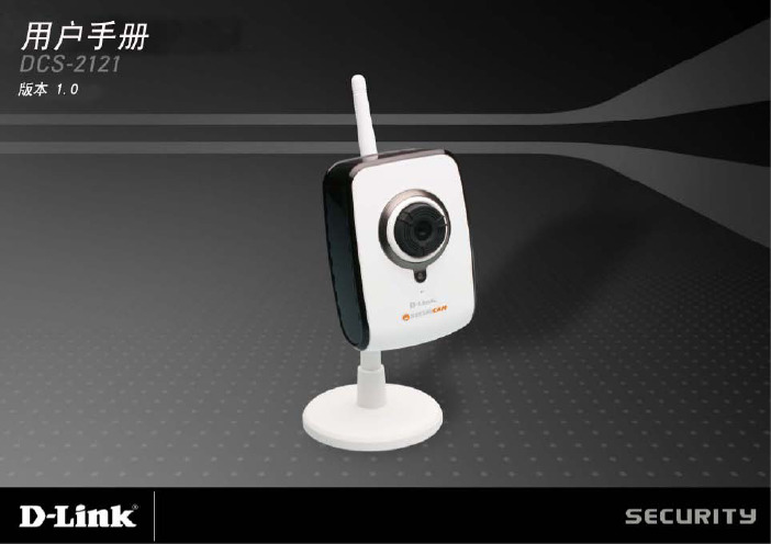
D-Link DCS-2121 说明书
目录包装清单....... (1)最低系统要求 (2)说明 (3) (4)特性和优势....................................................................................................................................硬件总览..... . (5)硬件安装 (7)连接天线............ .. (7)连接摄像设备 (7)连接以太网线缆 (8)连接电源适配器 (8)软件安装............... .. (9)安装安装精灵软件 (14)使用安装精灵 (17) (21)使用ffdshow ................................................................................................................................调整摄像头焦距 (24)使用WPS来安装无线连接 (25)使用配置菜单 (26)实施视频 (27)实时视频 > 摄像机 (27)安装 (28)安装> 安装精灵............................................................................................................................................................................................................ (28)安装> 网络安装 (29)安装> 无线............................................................................................................................ . (30)安装> 动态DNS (31)安装>镜像安装 (32)安装> 音频和视频............ (33)安装> 活动探测 (35)安装> 时间和日期 ...................................................................................................................... .. (36)安装> 记录 (37)安装> 抓拍 (39)安装> 数字输入 (41)维护............ . (42)维护> 设备管理 (42)维护> 备份和恢复 (43)维护> 固件升级 (44)状态 (45)状态>设备信息 (45)状态> 日志......................................................................................................................... . (46)帮助 (47).. (48)在路由器下安装 DCS-2121............ .........................................................................................................1)在网络上识别你的摄像设备................. . (48)2) 分配用于你的摄像设备的本地IP地址和端口 (49)3)打开HTTP端口....................................................................................................................... (50)4) 打开虚拟服务器端口来启用远程镜像查看 (52)在Internet上查看你的摄像设备 (53)在路由器下基于Internet 查看你的摄像设备 (53)常见问题 (54) (54)Internet摄像设备特性.....................................................................................................................................Internet摄像设备安装 (55) (57)怎样Ping你的IP地址时间区域表 (59)DI/DO输入技术规格 (60)技术规格 (61)包装清单如果丢失包裹中的任意一种物品,请与您的零售商联系。
2SD1260资料

1.5±0.1
s Features
1.5max.
10.5min. 2.0
1.1max.
0.8±0.1
0.5max.
s Absolute Maximum Ratings
Parameter Collector to base voltage Collector to 2SD1260 2SD1260A 2SD1260 Symbol VCBO VCEO VEBO ICP IC PC Tj Tstg
1:Base 2:Collector 3:Emitter N Type Package (DS)
(TC=25˚C)
Symbol ICBO ICEO IEBO VCEO hFE1 hFE2 VBE VCE(sat) fT ton tstg tf
*
Conditions VCE = 60V, IE = 0 VCE = 80V, IB = 0 VCE = 30V, IB = 0 VCE = 40V, IB = 0 VEB = 5V, IC = 0 IC = 30mA, IB = 0 VCE = 4V, IC = 1A VCE = 4V, IC = 2A VCE = 4V, IC = 2A IC = 2A, IB = 8mA VCE = 10V, IC = 0.5A, f = 1MHz IC = 2A, IB1 = 8mA, IB2 = –8mA, VCC = 50V
*h FE2
V V MHz µs µs µs
Rank classification
R Q P 1000 to 2500 2000 to 5000 4000 to 10000
- 1、下载文档前请自行甄别文档内容的完整性,平台不提供额外的编辑、内容补充、找答案等附加服务。
- 2、"仅部分预览"的文档,不可在线预览部分如存在完整性等问题,可反馈申请退款(可完整预览的文档不适用该条件!)。
- 3、如文档侵犯您的权益,请联系客服反馈,我们会尽快为您处理(人工客服工作时间:9:00-18:30)。
+0.2 9.70 -0.2
+0.1 0.80-0.1
+0.15 0.50 -0.15
0.127 max
+0.28 1.50 -0.1
+0.25 2.65 -0.1
+0.15 5.55 -0.15
2.3
+0.15 4 .60 -0.15
+ 0.1 0.600.1
1 Base 2 Collector 3 Emitter
Collector current IC (A)
20
3.0
iC(peak) IC(max)
PW = 10 ms
1.0
s 1m tion era ) C Op 。 DC = 25 (T C
10
0.3
。 Ta = 25 C 1 shot pulse 1
0
50 100 Case temperature TC (ϒ C)
■ ElectrБайду номын сангаасcal Characteristics Ta = 25℃
Parameter Collector- base breakdown voltage Collector- emitter breakdown voltage Emitter - base breakdown voltage Collector-base cut-off current Emitter cut-off current Collector-emitter saturation voltage Base - emitter saturation voltage Base - emitter voltage DC current gain Symbol VCBO VCEO VEBO ICBO IEBO VCE(sat) VBE(sat) VBE hFE Test Conditions Ic= 1 mA, IE= 0 Ic= 10 mA, RBE= ∞ IE= 1 mA, IC= 0 VCB= 35 V , IE= 0 VEB= 5V , IC=0 IC=2 A, IB=200mA IC=2 A, IB=200mA VCE= 2V, IC= 1.5 A VCE= 2 V, IC= 500mA VCE= 2V, IC= 1.5 A 60 20 Min 35 35 5 20 0.1 1 1.2 1.5 320 V uA V Typ Max Unit
0.3
0.1
0.03 IC = 10 IB Ta = 25。 C 0.1 0.3 1.0 Collector current IC (A) 3.0
Collector current IC (A)
VCE = 2 V 。 Ta = 25 C 0.4 0.8 1.2 1.6 2.0 Base to emitter voltage VBE (V)
■ Classification of hfe(1)
Type Range 2SD2121-B 60-120 2SD2121-C 100-200 2SD2121-D 160-320
NPN Transistors 2SD2121
■ Typical Characterisitics
30 Collector power dissipation PC (W) Maximum Collector Dissipation Curve 10 Area of Safe Operation
■ Absolute Maximum Ratings Ta = 25℃
Parameter Collector - Base Voltage Collector - Emitter Voltage Emitter - Base Voltage Collector Current - Continuous Collector Current - Pulse Collector Power Dissipation Junction Temperature Storage Temperature Range Symbol VCBO VCEO VEBO IC ICP PC TJ Tstg Rating 35 35 5 2.5 3 18 150 -55 to 150 A W ℃ V Unit
0.01 0.03
0
100
30
VCE = 2 V 。 Ta = 25 C 1.0 0.3 0.1 Collector current IC (A) 3.0
10 0.03
Collector to emitter saturation voltage VCE(sat) (V)
1.0
2.0 1.6 1.2 0.8 0.4
Typical Transfer Characteristics
10
8
DC current transfer ratio hFE
Collector current IC (A)
16 14 12
1,000
300
6
4 2 mA IB = 0 Ta = 25。 C 0 1 2 3 4 5 Collector to emitter voltage VCE (V) Collector to Emitter Saturation Voltage vs. Collector Current
Typical Output Characteristics
150
0.1
3 10 30 100 Collector to emitter voltage VCE (V)
DC Current Transfer Ratio vs. Collector Current
2.0 1.6 1.2 0.8 0.4
NPN Transistors 2SD2121
TO-252
+0.15 1.50 -0.15
Unit: mm
+0.15 6.50-0.15 +0.2 5.30-0.2
+0.1 2.30 -0.1 +0.8 0.50 -0.7
■ Features
3 .8 0
● Low frequency power amplifier ● Complementary to 2SB1407