TC1187VCT713, 规格书,Datasheet 资料
AT77C_datasheet

1.Features•Sensitive Layer Over a 0.35 µm CMOS Array •Image Zone: 0.4 x 14 mm = 0.02" x 0.55"•Image Array: 8 x 280 = 2240 pixels •Pixel Pitch: 50 µm x 50 µm = 500 dpi•Pixel Clock: up to 2 MHz Enabling up to 1780 Frames per Second •Die Size: 1.64 x 17.46 mm •Operating Voltage: 3V to 3.6V•Naturally Protected Against ESD: > 16 kV Air Discharge •Power Consumption: 16 mW at 3.3V , 1 MHz, 25°C •Operating Temperature Range: -40°C to +85°C•Chip-on-Board (COB), Chip-on-Board (COB) with Connector•Complies With the European Directive for Restriction of Hazardous Substances (RoHS Directive)2.Applications•PDA (Access Control, Data Protection)•Notebook, PC-add on (Access Control, e-business)•PIN Code Replacement•Automated Teller Machines, POS •Building Access•Electronic Keys (Cars, Home)•Portable Fingerprint Imaging for Law Enforcement •TV Access2Figure 2-1.FingerChip ® PackagesChip-on-board Package (COB)Chip-on-board Package with connector25364C–BIOM–3/07AT77C102BThe die attach is connected to pins 1, 7 and 21, and must be grounded. The FPL pin must be grounded.Table 2-1.Pin Description for Chip-on-Board Package: AT77C102B-CB01YVPin NumberName Type 1GND GND 2AVE Analog output 3AVO Analog output 4TPP Power 5TPE Digital input 6VCC Power 7GND GND 8RST Digital input 9PCLK Digital input 10OE Digital input 11ACKN Digital output 12De0Digital output 13Do0Digital output 14De1Digital output 15Do1Digital output 16De2Digital output 17Do2Digital output 18De3Digital output 19Do3Digital output 20FPL GND 21GNDGND35364C–BIOM–3/07AT77C102BNote:1.Ref. Connector: FH23-21S-0.3SHW (05) from HIROSE.Table 2-2.Pin Description for COB with Connector Package: AT77C102B-CB02YV (1)Pin NumberName Type 1FPL GND2Not connected 3Not connected4DE3Digital output 5DO3Digital output 6DE2Digital output 7DO2Digital output 8DE1Digital output 9DO1Digital output 10DE0Digital output 11DO0Digital output 12AVE Analog output 13AVO Analog output 14TPP Power 15TPE Digital input 16VCC Power 17GND GND 18RST Digital input 19PCLK Digital input 20OE Digital input 21ACKNDigital output45364C–BIOM–3/07AT77C102BFigure 2-2.COB with Flex (1)Figure 2-3.Flex Output SideNote: 1.Flex is not provided by Atmel.Flex with metallizations upFlex with metallizations down23 1Flex Output(FingerChip Connector Side)Metallizations Up55364C–BIOM–3/07AT77C102B3.DescriptionThe AT77C102B is part of the Atmel FingerChip monolithic fingerprint sensor family for which no optics, no prism and no light source are required.The AT77C102B is a single-chip, high-performance, low-cost sensor based on temperature physical effects for fingerprint sensing.The AT77C102B has a linear shape, which captures a fingerprint image by sweeping the finger across the sensing area. After capturing several images, Atmel proprietary software can recon-struct a full 8-bit fingerprint image.The AT77C102B has a small surface combined with CMOS technology, and a Chip-on-Board package assembly. These facts contribute to a low-cost device.The device delivers a programmable number of images per second, while an integrated analog-to-digital converter delivers a digital signal adapted to interfaces such as an EPP parallel port, a USB microcontroller or directly to microprocessors. No frame grabber or glue interface is there-fore necessary to send the frames. These facts make AT77C102B an easy device to include in any system for identification or verification applications.Table 3-1.Absolute Maximum RatingsParameterSymbol CommentsValue Positive supply voltage V CC GND to 4.6Note: Stresses beyond those listed under “Absolute Maximum Ratings” may cause permanent damage to the device. These are stress ratings only and functional operation of the device at these or any other conditions beyond those indicated in the operational sections of this specification is not implied. Exposure to absolutemaximum rating conditions for extended periods may affect device reliability.T emperature stabilization power TPP GND to 4.6Front plane FPL GND to V CC +0.5Digital input voltage RST PCLKGND to V CC +0.5Storage temperature T stg -50 to +95Lead temperature(soldering, 10 seconds)T leadsDo not solder ForbiddenTable 3-2.Recommended Conditions Of UseParameterSymbol CommentsMin Typ Max Unit Positive supply voltage V CC 3V3.3V 3.6VV Front plane FPLMust be grounded GND V Digital input voltage CMOS levels V Digital output voltage CMOS levelsV Digital load C L 50pF Analog loadC A R A Not connected pF k ΩOperating temperature range T amb V grade-40°C to +85°C°C Maximum current on TPPITPP100mA65364C–BIOM–3/07AT77C102BTable 3-3.ResistanceParameter Min ValueStandard MethodESDOn pins. HBM (Human Body Model) CMOS I/O 2 kV MIL-STD-883 - method 3015.7On die surface (Zapgun) Air discharge±16 kVNF EN 6100-4-2Mechanical AbrasionNumber of cycles without lubricant multiply by an estimated factor of 20 for correlation with a real finger 200 000MIL E 12397BChemical ResistanceCleaning agent, acid, grease, alcohol, diluted acetone4 hours Internal methodTable 3-4.SpecificationsExplanation Of Test LevelsI 100% production tested at +25°CII100% production tested at +25°C, and sample tested at specified temperatures (AC testing done on sample)III Sample tested only IV Parameter is guaranteed by design and/or characterization testing V Parameter is a typical value onlyVI 100% production tested at temperature extremes D100% probe tested on wafer at T amb = +25°CTable 3-5.Physical ParameterParameter Test LevelMinTyp MaxUnit Resolution IV 50µm SizeIV 8 x 280Pixel Yield: number of bad pixels I 5Bad pixelsEquivalent resistance on TPP pinI253045Ω.Note:1.With I OL = 1 mA and I OH = -1 mATable 3-6.3.3V Power supplyThe following characteristics are applicable to the operating temperature -40°C ≤ Ta ≤ +85°C Typical conditions are: V CC = +3.3 V; T amb = 25°C; F PCLK = 1 MHz; Duty cycle = 50% C load 120 pF on digital outputs, analog outputs disconnected unless otherwise specifiedParameterSymbolTest LevelMinTypMaxUnitPower Requirements Positive supply voltageV CC 3.0 3.3 3.6V Active current on V CC pin, 1 MHzCurrent on V CC pin, in static mode C load = 0 pF I CC I IV 5475mA mA Power dissipation on V CC C load = 0P CC I IV 16132518mW mW Current on V CC in NAP mode I CCNAP I10µAAnalog Output Voltage range V AVxIV 0 2.9VDigital Inputs Logic compatibility CMOSLogic “0” voltage V IL I 00.8V Logic “1” voltage V IH I 2.3VCC V Logic “0” current I IL I -100µA Logic “1”current I IH I 010µA TPE logic “0” voltage I IL TPE 1-100µA TPE logic “1” voltage I IH TPE1300µADigital Outputs Logic compatibility CMOSLogic “0” voltage (1)V OL I 0.6V Logic “1” voltage (1)V OHI2.4V75364C–BIOM–3/07AT77C102B85364C–BIOM–3/07AT77C102BFigure 3-1.ResetTable 3-7.Switching PerformancesThe following characteristics are applicable to the operating temperature -40°C ≤ Ta ≤ +85°C Typical conditions are: nominal voltage; T amb = 25°C; F PCLK = 1 MHz; Duty cycle = 50% C load 120 pF on digital and analog outputs unless otherwise specifiedParameter Symbol Test LevelMin Typ Max Unit Clock frequency f PCLK I 0.512MHz Clock pulse width (high)t HCLK I 250ns Clock pulse width (low)t LCLK I 250ns Clock setup time (high)/reset falling edge t Setup I 0ns No data change t NOOE IV 100ns Reset pulse width hight HRSTIV50nsTable 3-8.3.3V ±10% Power SupplyParameterSymbol Test LevelMinTypMax Unit Output delay from PCLK to ACKN rising edge t PLHACKN I 145ns Output delay from PCLK to ACKN falling edge t PHLACKN I 145ns Output delay from PCLK to data output Dxi t PDAT A I 120ns Output delay from PCLK to analog output AVx t P AVIDEO I 250ns Output delay from OE to data high-Z t DAT AZ IV 34ns Output delay from OE to data outputt ZDAT AIV47ns95364C–BIOM–3/07AT77C102BFigure 3-2.Read One Byte/Two PixelsFigure 3-3.Output Enable105364C–BIOM–3/07AT77C102BFigure 3-4.No Data ChangeNote:OE must not change during TNOOE after the PCLK falls. This is to ensure that the output drivers of the data are not driving cur-rent, so as to reduce the noise level on the power supply.Figure 3-5.AT77C102B Block Diagram3.1Functional DescriptionThe circuit is divided into two main sections: sensor and data conversion. One particular column among 280 plus one is selected in the sensor array (1), then each pixel of the selected column sends its electrical information to the amplifiers (2) [one per line], then two lines at a time are selected (odd and even) so that two particular pixels send their information to the input of two 4-bit analog-to-digital converters (3), so two pixels can be read for each clock pulse (4).115364C–BIOM–3/07AT77C102BFigure 3-6.Functional Description3.2SensorEach pixel is a sensor in itself. The sensor detects a temperature difference between the begin-ning of an acquisition and the reading of the information: this is the integration time. The integration time begins with a reset of the pixel to a predefined initial state. Note that the integra-tion time reset has nothing to do with the reset of the digital section.Then, at a rate depending on the sensitivity of the pyroelectric layer, on the temperature varia-tion between the reset and the end of the integration time, and for the duration of the integration time, electrical charges are generated at the pixel level.3.3Analog-to-digital Converter/ Reconstructing an 8-bit Fingerprint ImageAn analog-to-digital converter (ADC) is used to convert the analog signal coming from the pixel into digital data that can be used by a processor.As the data rate for the parallel port and the USB is in the range of 1 MB per second, and at least a rate of 500 frames per second is needed to reconstruct the image with a fair sweeping speed of the finger, two 4-bit ADCs have been used to output two pixels at a time on one byte.3.4Start SequenceA reset is not necessary between each frame acquisition.The start sequence must consist in:1.Setting the RST pin to high.2.Setting the RST pin to low.3.Sending 4 clock pulses (due to pipe-line).4.Sending clock pulses to skip the first frame.Note that after a reset it is recommended to skip the first 200 slices to stabilize the acquisition.Figure 3-7.Start Sequence125364C–BIOM–3/07AT77C102B3.5Reading the FramesA frame consists of 280 true columns plus one dummy column of eight pixels. As two pixels are output at a time, a system must send 281 x 4 = 1124 clock pulses to read one frame.Reset must be low when reading the frames.3.6Read One Byte/Output EnableThe clock is taken into account on its falling edge and data is output on its rising edge.For each clock pulse, after the start sequence, a new byte is output on the Do0-3 and De0-3 pins. This byte contains two pixels: 4-bit on Do0-3 (odd pixels), 4-bit on De0-3 (even pixels).To output the data, the output enable (OE) pin must be low. When OE is high, the Do0-3 and De0-3 pins are in high-impedance state. This facilitates an easy connection to a microprocessor bus without additional circuitry since the data output can be enabled using a chip select signal. Note that the AT77C102B always sends data: there is no data exchange to switch to read/write mode.3.7Power Supply NoiseIMPORTANT: When a falling edge is applied on OE (that is when the Output Enable becomes active), then some current is drained from the power supply to drive the eight outputs, producing some noise. It is important to avoid such noise just after the PCLK clock’s falling edge, when the pixels’ information is evaluated: the timing diagram (Figure 3-2) and time T NOOE define the inter-val time when the power supply must be as quiet as possible.3.8Video OutputAn analog signal is also available on pins AVE and AVO. Note that video output is available one clock pulse before the corresponding digital output (one clock pipe-line delay for the analog to digital conversion).3.9Pixel OrderAfter a reset, pixel 1 is located on the upper left corner, looking at the chip with bond pads to the right. For each column of eight pixels, pixels 1, 3, 5 and 7 are output on odd data Do0-3 pins, and pixels 2, 4, 6 and 8 are output on even data De0-3 pins. The Most Significant Bit (MSB) is bit 3, and the Least Significant Bit is bit 0.Figure 3-8.Pixel Order135364C–BIOM–3/07AT77C102B3.10Synchronization: The Dummy ColumnA dummy column has been added to the sensor to act as a specific pattern to detect the first pixel. Therefore, 280 true columns plus one dummy column are read for each frame.The four bytes of the dummy column contain a fixed pattern on the first two bytes, and tempera-ture information on the last two bytes.Note:x represents 0 or 1The sequence 111X0000 111X0000 appears on every frame (exactly every 1124 clock pulses), so it is an easy pattern to recognize for synchronization purposes.3.11ThermometerThe dummy bytes DB3 and DB4 contain some internal temperature information.The even nibble nnnn in DB3 can be used to measure an increase or decrease of the chip’s tem-perature, using the difference between two measures of the same physical device. The following table gives values in Kelvin.Table 1. Dummy Column DescriptionDummy Byte Odd Even Dummy Byte 1 DB1: 111X 0000 Dummy Byte 2 DB2: 111X 0000 Dummy Byte 3 DB3: rrrr nnnn Dummy Byte 4 DB4:ttttppppTable 1. Temperature Tablennnn Decimal nnnn Binary Temperature differential with code 8in Kelvin151111> 11.21411108.41311017121100 5.6111011 4.2101010 2.891001 1.481000070111-1.460110-2.850101-4.240100-5.630011-720010-8.410001-11.200000< -16.8145364C–BIOM–3/07AT77C102BFor code 0 and 15, the absolute value is a minimum (saturation).When the image contrast becomes faint because of a low temperature difference between the finger and the sensor, it is recommended to use the temperature stabilization circuitry to increase the temperature by two codes (that is from 8 to 10), so as to obtain a sensor increase of at least >1.4 Kelvin. This enables enough contrast to obtain a proper fingerprint reconstruction.3.12Integration Time and Clock JitterThe AT77C102B is not very sensitive to clock jitters (clock variations). The most important requirement is a regular integration time that ensures the frame reading rate is also as regular as possible, so as to obtain consistent fingerprint slices.If the integration time is not regular, the contrast can vary from one frame to another.Note that it is possible to introduce some waiting time between each set of 1124 clock pulses, but the overall time of one frame read must be regular. This waiting time is generally the time needed by the processor to perform some calculation over the frame (to detect the finger, for instance).Figure 3-9.Read One FrameFigure 3-10.Regular Integration Time3.13Power Management 3.14Nap ModeSeveral strategies are possible to reduce power consumption when the device is not in use.The simplest and most efficient is to cut the power supply using external means.A nap mode is also implemented in the AT77C102B. To activate this nap mode, you must:1.Set the reset RST pin to high. By doing this, all analog sections of the device are inter-nally powered down.2.Set the clock PCLK pin to high (or low), thus stopping the entire digital section.3.Set the TPE pin to low to stop the temperature stabilization feature.4.Set the Output Enable OE pin to high, so that the output is forced in HiZ.155364C–BIOM–3/07AT77C102BFigure 3-11.Nap ModeIn nap mode, all internal transistors are in shut mode. Only leakage current is drained in the power supply, generally less than the tested value.3.15Static Current ConsumptionWhen the clock is stopped (set to 1) and the reset is low (set to 0), the device’s analog sections drain some current, whereas, if the outputs are connected to a standard CMOS input, the digital section does not consume any current (no current is drained in the I/O). In this case the typical current value is 5 mA. This current does not depend on the voltage (it is almost the same from 3 to 3.6V).3.16Dynamic Current ConsumptionWhen the clock is running, the digital sections, and particularly the outputs if they are heavily loaded, consume current. In any case, the current should be less than the testing machine (120 pF load on each I/O), and a maximum of 50 pF is recommended.The AT77C102B, running at about 1 MHz, consumes less than 7 mA on the V CC pin.3.17Temperature Stabilization Power Consumption (TPP Pin)When the TPE pin is set to 1, current is drained via the TPP pin. The current is limited by the internal equivalent resistance given in Table 3-4 on page 6 and a possible external resistor. Most of the time, TPE is set to 0 and no current is drained in TPP. When the image contrast becomes low because of a low temperature differential (less than 1 Kelvin), then it is recom-mended to set TPE to 1 for a short time so that the dissipated power in the chip elevates the temperature, allowing contrast recovery. The necessary time to increase the chip’s temperature by one Kelvin depends on the dissipated power, the thermal capacity of the silicon sensor and the thermal resistance between the sensor and its surroundings. As a rule of thumb, dissipating 300 mW in the chip elevates the temperature by 1 Kelvin in one second. With the 30Ω typical value, 300 mW is 3V applied on TPP. If the power supply is 3.6V, an external resistor must be added in the application to limit the current under 100 mA.165364C–BIOM–3/07AT77C102B4.Packaging: Mechanical DataFigure 4-2.Product Reference: AT77C102B-CB01YV — Bottom View (all dimensions in mm)175364C–BIOM–3/07AT77C102BFigure 4-3.Product Reference: AT77C102B-CB02YV4.1Package Information4.1.1Electrical DisturbancesWhen looking at the fingerchip device from the top with the glob top to the right, the right edge must never be in contact with customer casing or any component to avoid electrical disturbances.Figure 4-4.Epoxy OverflowMaximum epoxy overflow width: 0.55 mm on the die edge.Maximum epoxy overflow thickness: 0.33 mm.Note:Refer to Figure 4-1 on page 16.185364C–BIOM–3/07AT77C102B5.Ordering Information5.1Package Device195364C–BIOM–3/07AT77C102BRevision HistoryDoc. Rev.Date Comments5364C 3/2007Equivalent resistance on TPP pin ranges reduced page 6 table 3.55364B 1/2007Connector change in production for CB02: FH18 to FH23.p3 & p17 fig 4-3: Connector reference & Mechanical data plan for CB02 updated.5364AInitial Document Release5364C–BIOM–3/07©2007 Atmel Corporation. All rights reserved. Atmel®, logo and combinations thereof, Everywhere You Are®, FingerChip®, and others are reg-istered trademarks or trademarks of Atmel Corporation or its subsidiaries. Other terms and product names may be trademarks of others.Disclaimer: The information in this document is provided in connection with Atmel products. No license, express or implied, by estoppel or otherwise, to any intellectual property right is granted by this document or in connection with the sale of Atmel products. EXCEPT AS SET FORTH IN ATMEL ’S TERMS AND CONDI-TIONS OF SALE LOCATED ON ATMEL ’S WEB SITE, ATMEL ASSUMES NO LIABILITY WHATSOEVER AND DISCLAIMS ANY EXPRESS, IMPLIED OR STATUTORY WARRANTY RELATING TO ITS PRODUCTS INCLUDING, BUT NOT LIMITED TO, THE IMPLIED WARRANTY OF MERCHANTABILITY, FITNESS FOR A PARTICULAR PURPOSE, OR NON-INFRINGEMENT. IN NO EVENT SHALL ATMEL BE LIABLE FOR ANY DIRECT, INDIRECT, CONSEQUENTIAL, PUNITIVE, SPECIAL OR INCIDEN-TAL DAMAGES (INCLUDING, WITHOUT LIMITATION, DAMAGES FOR LOSS OF PROFITS, BUSINESS INTERRUPTION, OR LOSS OF INFORMATION) ARISING OUT OF THE USE OR I NABI LI TY TO USE THI S DOCUMENT, EVEN I F ATMEL HAS BEEN ADVI SED OF THE POSSI BI LI TY OF SUCH DAMAGES. Atmel makes no representations or warranties with respect to the accuracy or completeness of the contents of this document and reserves the right to make changes to specifications and product descriptions at any time without notice. Atmel does not make any commitment to update the information contained herein. Unless specifically provided otherwise, Atmel products are not suitable for, and shall not be used in, automotive applications. Atmel’s products are not intended, authorized, or warranted for use as components in applications intended to support or sustain life.Atmel CorporationAtmel Operations2325 Orchard Parkway San Jose, CA 95131, USA Tel: 1(408) 441-0311Fax: 1(408) 487-2600Regional HeadquartersEuropeAtmel SarlRoute des Arsenaux 41Case Postale 80CH-1705 Fribourg SwitzerlandTel: (41) 26-426-5555Fax: (41) 26-426-5500AsiaRoom 1219Chinachem Golden Plaza 77 Mody Road Tsimshatsui East Kowloon Hong KongTel: (852) 2721-9778Fax: (852) 2722-1369Japan9F, Tonetsu Shinkawa Bldg.1-24-8 ShinkawaChuo-ku, Tokyo 104-0033JapanTel: (81) 3-3523-3551Fax: (81) 3-3523-7581Memory2325 Orchard Parkway San Jose, CA 95131, USA Tel: 1(408) 441-0311Fax: 1(408) 436-4314Microcontrollers2325 Orchard Parkway San Jose, CA 95131, USA Tel: 1(408) 441-0311Fax: 1(408) 436-4314La Chantrerie BP 7060244306 Nantes Cedex 3, France Tel: (33) 2-40-18-18-18Fax: (33) 2-40-18-19-60ASIC/ASSP/Smart CardsZone Industrielle13106 Rousset Cedex, France Tel: (33) 4-42-53-60-00Fax: (33) 4-42-53-60-011150 East Cheyenne Mtn. Blvd.Colorado Springs, CO 80906, USA Tel: 1(719) 576-3300Fax: 1(719) 540-1759Scottish Enterprise Technology Park Maxwell BuildingEast Kilbride G75 0QR, Scotland Tel: (44) 1355-803-000Fax: (44) 1355-242-743RF/AutomotiveTheresienstrasse 2Postfach 353574025 Heilbronn, Germany Tel: (49) 71-31-67-0Fax: (49) 71-31-67-23401150 East Cheyenne Mtn. Blvd.Colorado Springs, CO 80906, USA Tel: 1(719) 576-3300Fax: 1(719) 540-1759Biometrics Product LineAvenue de Rochepleine BP 12338521 Saint-Egreve Cedex, France Tel: (33) 4-76-58-47-50Fax: (33) 4-76-58-47-60Literature Requests/literature。
CN3717_datasheet

铅酸电池充电 不间断电源 备用电池应用 便携式工业和医疗仪器 独立电池充电器
特点:
宽输入电压范围:7.5V 到 28V 对铅酸电池进行完整的充电管理 过充电和浮充电电压由外部电阻
分压网络设置 充电电流达 5A PWM 开关频率:300KHz 恒流充电电流由外部电阻设置 对深度放电的电池进行涓流充电 过充点结束电流由外部电阻设置 电池温度监测功能 自动再充电功能 双状态指示 软启动功能 电池端过压保护 工作环境温度:-40℃ 到 +85℃ 采用 16 管脚 TSSOP 封装 产品无铅,无卤素元素,满足 RoHS
超出以上所列的极限参数可能造成器件的永久损坏。以上给出的仅仅是极限范围,在这样的极限条件下 工作,器件的技术指标将得不到保证,长期在这种条件下还会影响器件的可靠性。
Rev 1.1
3
如韵电子 CONSONANCE
电气特性:
(VCC=15V,TA=-40℃ 到 85℃,除非另有注明)
113 13 5
1.06 0.98
典型
6 1.7 40 120
23 10 75.6% 93.6% 82.2% 1.08 1
最大 28 7.3 2.2 260 127 33 15
1.1 1.02
单位 V V mA nA
mV
uA
VOC (注 1)
3.64 3.69
3.74 V
-5.56mV
/℃
3.46 -5mV
Iup Vthh
TEMP 管脚电压上升
比较器低端阈值
Vthl TEMP 管脚电压下降
CHRG 管脚
CHRG管脚下拉电流 CHRG管脚漏电流 DONE 管脚
CC8800 系列 CMTS 产品规格书说明书
CC8800系列CMTS产品规格书(CC8800-F-U2)鼎点视讯科技有限公司.资料版本:R02发布日期:2019.01修订记录日期修订版本描述2018.05 R01 初版发布2019.01 R02 更新了上联口规格及支持的光模块规格声明Copyright ©2001~2019北京数码视讯科技集团鼎点视讯科技有限公司版权所有,保留一切权利。
未经本公司书面许可,任何单位和个人不得擅自摘抄、复制本书内容的部分或全部,并不得以任何形式传播。
TOPVISION、Sumavision、、、、、、均为北京数码视讯科技集团的商标。
对于本手册中出现的其它公司的商标、产品标识及商品名称,由各自权利人拥有。
由于产品版本升级或其它原因,本手册内容会不定期进行更新。
除非另有约定,本手册仅作为使用指导。
本手册中的所有陈述、信息和建议不构成任何明示或暗示的担保。
技术支持北京数码视讯科技集团鼎点视讯科技有限公司为客户提供全方位的技术支持。
通过北京数码视讯科技集团代理商购买产品的用户,请直接与销售代理商联系。
向鼎点视讯科技有限公司购买产品的用户,可与就近的数码视讯/鼎点视讯办事处联系,也可直接与鼎点视讯科技有限公司联系。
用户服务热线:联系电话:+86-10-58858351(周一至周五8:30-17:30)传真:+86-10-58858592公司地址:北京海淀区上地东路1号盈创动力大厦A2座6层邮编:100085登录网址:或目录第1章产品简介 (1)1.1 产品介绍 (1)1.2 产品特点 (1)第2章性能与规格 (3)2.1 简介 (3)2.2 整机规格 (4)2.3 DOCSIS模块 (4)2.4 电源模块 (8)2.5 射频模块 (9)2.6 (可选)CWDM组件规格 (10)2.7 (可选)工业级SFP+光模块 (11)2.7.1 10GE以太网光模块 (11)2.7.2 ONU侧10G EPON光模块 (12)2.7.3 ONU侧XG-PON光模块 (12)第1章产品简介DOCSIS定义了一种利用有线同轴网络中传输数据业务的规范,是稳定、可靠的运营级同轴网络国际标准,并且经过了多年的实际运营检验。
TLC7135中文资料

PRODUCTION DATA information is current as of publication date. Products conform to specifications per the terms of Texas Instruments standard warranty. Production processing does not necessarily include testing of all parameters.元器件交易网IMPORTANT NOTICETexas Instruments (TI) reserves the right to make changes to its products or to discontinue any semiconductorproduct or service without notice, and advises its customers to obtain the latest version of relevant informationto verify, before placing orders, that the information being relied on is current.TI warrants performance of its semiconductor products and related software to the specifications applicable atthe time of sale in accordance with TI’s standard warranty. Testing and other quality control techniques areutilized to the extent TI deems necessary to support this warranty. Specific testing of all parameters of eachdevice is not necessarily performed, except those mandated by government requirements.Certain applications using semiconductor products may involve potential risks of death, personal injury, orsevere property or environmental damage (“Critical Applications”).TI SEMICONDUCTOR PRODUCTS ARE NOT DESIGNED, INTENDED, AUTHORIZED, OR WARRANTEDTO BE SUITABLE FOR USE IN LIFE-SUPPORT APPLICATIONS, DEVICES OR SYSTEMS OR OTHERCRITICAL APPLICATIONS.Inclusion of TI products in such applications is understood to be fully at the risk of the customer. Use of TIproducts in such applications requires the written approval of an appropriate TI officer. Questions concerningpotential risk applications should be directed to TI through a local SC sales office.In order to minimize risks associated with the customer’s applications, adequate design and operatingsafeguards should be provided by the customer to minimize inherent or procedural hazards.TI assumes no liability for applications assistance, customer product design, software performance, orinfringement of patents or services described herein. Nor does TI warrant or represent that any license, eitherexpress or implied, is granted under any patent right, copyright, mask work right, or other intellectual propertyright of TI covering or relating to any combination, machine, or process in which such semiconductor productsor services might be or are used.Copyright © 1995, Texas Instruments Incorporated。
TC1186-1.8VCT713中文资料

© 2007 Microchip Technology Inc.DS21350D-page 1TC1054/TC1055/TC1186Features•Low Ground Current for Longer Battery Life •Low Dropout Voltage•Choice of 50mA (TC1054), 100mA (TC1055) and 150mA (TC1186) Output •High Output Voltage Accuracy•Standard or Custom Output Voltages:- 1.8V, 2.5V, 2.6V, 2.7V, 2.8V, 2.85V, 3.0V, 3.3V, 3.6V, 4.0V, 5.0V•Power-Saving Shutdown Mode•ERROR Output Can Be Used as a Low Battery Detector or Microcontroller Reset Generator •Overcurrent and Overtemperature Protection •5-Pin SOT-23 Package•Pin Compatible Upgrades for Bipolar RegulatorsApplications•Battery Operated Systems •Portable Computers •Medical Instruments •Instrumentation•Cellular/GSM/PHS Phones•Linear Post-Regulators for SMPS •PagersTypical ApplicationGeneral DescriptionThe TC1054, TC1055 and TC1186 are high accuracy (typically ±0.5%) CMOS upgrades for older (bipolar)low dropout regulators. Designed specifically for battery-operated systems, the devices’ CMOS construction minimizes ground current, extending battery life. Total supply current is typically 50µA at full load (20 to 60 times lower than in bipolar regulators).The devices’ key features include low noise operation,low dropout voltage – typically 85mV (TC1054),180mV (TC1055) and 270mV (TC1186) at full load —and fast response to step changes in load. An error output (ERROR) is asserted when the devices are out-of-regulation (due to a low input voltage or excessive output current). ERROR can be used as a low battery warning or as a processor RESET signal (with the addition of an external RC network). Supply current is reduced to 0.5µA (max), with both V OUT and ERROR disabled when the shutdown input is low. The devices incorporate both over-temperature and over-current protection.The TC1054, TC1055 and TC1186 are stable with an output capacitor of only 1µF and have a maximum output current of 50mA, 100mA and 150mA,respectively. For higher output current regulators,please refer to the TC1173 (I OUT = 300mA) data sheet (DS21632).Package TypeTC1054TC1055TC1186V OUT GND1µF+V IN V IN V OUT15243SHDN Shutdown Control(from Power Control Logic)ERRORERROR1M ΩNOTE: 5-Pin SOT-23 is equivalent to the EIAJ (SC-74A)514235-Pin SOT-23TC1054TC1055TC1186V OUT ERRORSHDN GNDV IN50mA, 100mA and 150mA CMOS LDOs with Shutdownand ERROR OutputTC1054/TC1055/TC1186DS21350D-page 2© 2007 Microchip Technology Inc.1.0ELECTRICALCHARACTERISTICSAbsolute Maximum Ratings †Input Voltage....................................................................6.5V Output Voltage .....................................(-0.3V) to (V IN + 0.3V)Power Dissipation .........................Internally Limited (Note 6)Maximum Voltage on Any Pin ...................V IN +0.3V to -0.3V Operating Junction Temperature Range..-40°C < T J < 125°C Storage Temperature.....................................-65°C to +150°C† Stresses above those listed under "Absolute Maximum Ratings" may cause permanent damage to the device. These are stress ratings only and functional operation of the device at these or any other conditions above those indicated in the operation sections of the specifications is not implied.Exposure to Absolute Maximum Rating conditions for extended periods may affect device reliability.DC CHARACTERISTICSElectrical Specifications: Unless otherwise noted, V IN = V OUT + 1V, I L = 100µA, C L = 3.3µF, SHDN > V IH , T A = +25°C.Boldface type specifications apply for junction temperatures of -40°C to +125°C.ParametersSym Min Typ Max Units ConditionsInput Operating Voltage V IN 2.7— 6.0V Note 8Maximum Output CurrentI OUT MAX50100150——————mATC1054TC1055TC1186Output VoltageV OUT V R – 2.5% V R ±0.5%V R + 2.5%VNote 1V OUT Temperature Coefficient TCV OUT ——2040——ppm/°C Note 2Line Regulation ΔV OUT /ΔV IN —0.050.35%(V R + 1V) ≤ V IN ≤ 6V Load Regulation:TC1054; TC1055TC1186ΔV OUT /V OUT——0.50.523%(Note 3)I L = 0.1mA to I OUT MAX I L = 0.1mA to I OUT MAX Dropout Voltage:TC1055; TC1186TC1186V IN -V OUT—————26585180270——120250400mVI L = 100µA I L = 20mA I L = 50mA I L = 100mAI L = 150mA (Note 4)Supply CurrentI IN —5080µA SHDN = V IH , I L = 0µA (Note 9)Shutdown Supply Current I INSD —0.050.5µA SHDN = 0V Power Supply Rejection Ratio PSRR —64—dB f ≤ 1kHz Output Short Circuit Current I OUT SC —300450mA V OUT = 0V Thermal Regulation ΔV OUT /ΔP D—0.04—V/W Notes 5,6Thermal Shutdown Die TemperatureT SD —160—°C Thermal Shutdown HysteresisΔT SD—10—°CNote 1:V R is the regulator output voltage setting. For example: V R = 1.8V, 2.5V, 2.7V, 2.85V, 3.0V, 3.3V, 3.6V, 4.0V, 5.0V.2:3:Regulation is measured at a constant junction temperature using low duty cycle pulse testing. Load regulation is testedover a load range from 0.1mA to the maximum specified output current. Changes in output voltage due to heating effects are covered by the thermal regulation specification.4:Dropout voltage is defined as the input to output differential at which the output voltage drops 2% below its nominalvalue.5:Thermal Regulation is defined as the change in output voltage at a time T after a change in power dissipation is applied,excluding load or line regulation effects. Specifications are for a current pulse equal to I L MAX at V IN = 6V for T = 10ms.6:The maximum allowable power dissipation is a function of ambient temperature, the maximum allowable junctiontemperature and the thermal resistance from junction-to-air (i.e., T A , T J , θJA ). Exceeding the maximum allowable power dissipation causes the device to initiate thermal shutdown. Please see Section 5.0 “Thermal Considerations”, “Ther-mal Considerations”, for more details.7:Hysteresis voltage is referenced by V R .8:The minimum V IN has to justify the conditions: V IN ≥ V R + V DROPOUT and V IN ≥ 2.7V for I L = 0.1mA to I OUT MAX .9:Apply for junction temperatures of -40C to +85C.TC V OUT = (V OUT MAX – V OUT MIN )x 106V OUT x ΔT© 2007 Microchip Technology Inc.DS21350D-page 3TC1054/TC1055/TC1186Output Noise eN—260—nV/√Hz I L = I OUT MAXSHDN InputSHDN Input High Threshold V IH 45——%V IN V IN = 2.5V to 6.5V SHDN Input Low Threshold V IL——15%V INV IN = 2.5V to 6.5VERROR OutputMinimum V IN Operating Voltage V IN MIN 1.0——V Output Logic Low Voltage V OL ——400mV 1mA Flows to ERROR ERROR Threshold Voltage V TH —0.95 x V R—V See Figure 4-2ERROR Positive Hysteresis V HYS —50—mV Note 7V OUT to ERROR Delayt DELAY—2.5—msV OUT falling from V R to V R - 10%DC CHARACTERISTICS (CONTINUED)Electrical Specifications: Unless otherwise noted, V IN = V OUT + 1V, I L = 100µA, C L = 3.3µF, SHDN > V IH , T A = +25°C.Boldface type specifications apply for junction temperatures of -40°C to +125°C.ParametersSym Min Typ Max UnitsConditionsNote 1:V R is the regulator output voltage setting. For example: V R = 1.8V, 2.5V, 2.7V, 2.85V, 3.0V, 3.3V, 3.6V, 4.0V, 5.0V.2:3:Regulation is measured at a constant junction temperature using low duty cycle pulse testing. Load regulation is testedover a load range from 0.1mA to the maximum specified output current. Changes in output voltage due to heating effects are covered by the thermal regulation specification.4:Dropout voltage is defined as the input to output differential at which the output voltage drops 2% below its nominalvalue.5:Thermal Regulation is defined as the change in output voltage at a time T after a change in power dissipation is applied,excluding load or line regulation effects. Specifications are for a current pulse equal to I L MAX at V IN = 6V for T = 10ms.6:The maximum allowable power dissipation is a function of ambient temperature, the maximum allowable junctiontemperature and the thermal resistance from junction-to-air (i.e., T A , T J , θJA ). Exceeding the maximum allowable power dissipation causes the device to initiate thermal shutdown. Please see Section 5.0 “Thermal Considerations”, “Ther-mal Considerations”, for more details.7:Hysteresis voltage is referenced by V R .8:The minimum V IN has to justify the conditions: V IN ≥ V R + V DROPOUT and V IN ≥ 2.7V for I L = 0.1mA to I OUT MAX .9:Apply for junction temperatures of -40C to +85C.TC V OUT = (V OUT MAX – V OUT MIN )x 106OUTTC1054/TC1055/TC1186DS21350D-page 4© 2007 Microchip Technology Inc.2.0TYPICAL PERFORMANCE CURVESNote: Unless otherwise indicated, V IN = V OUT + 1V, I L = 100µA, C L = 3.3µF, SHDN > V IH , T A = +25°C.FIGURE 2-1:Dropout Voltage vs. Temperature (I LOAD = 10mA).FIGURE 2-2:Dropout Voltage vs. Temperature (I LOAD = 100mA).FIGURE 2-3:Ground Current vs. V IN(I LOAD = 10mA).FIGURE 2-4:Dropout Voltage vs. Temperature (I LOAD = 50mA).FIGURE 2-5:Dropout Voltage vs. Temperature (I LOAD = 150mA).FIGURE 2-6:Ground Current vs. V IN(I LOAD = 100mA).Note:The graphs and tables provided following this note are a statistical summary based on a limited number of samples and are provided for informational purposes only. The performance characteristics listed herein are not tested or guaranteed. In some graphs or tables, the data presented may be outside the specified operating range (e.g., outside specified power supply range) and therefore outside the warranted range.TC1054/TC1055/TC1186 Note: Unless otherwise indicated, V IN = V OUT + 1V, I L = 100µA, C L = 3.3µF, SHDN > V IH, T A = +25°C.FIGURE 2-7:Ground Current vs. V IN (I LOAD = 150mA).FIGURE 2-8:V OUT vs. V IN(I LOAD=100mA).FIGURE 2-9:V OUT vs. V IN(I LOAD=150mA).FIGURE 2-10:V OUT vs. V IN(I LOAD=0mA).FIGURE 2-11:Output Voltage (3.3V) vs. Temperature (I LOAD = 10mA).FIGURE 2-12:Output Voltage (5V) vs. Temperature (I LOAD = 10mA).© 2007 Microchip Technology Inc.DS21350D-page 5TC1054/TC1055/TC1186DS21350D-page 6© 2007 Microchip Technology Inc.Note: Unless otherwise indicated, V IN = V OUT + 1V, I L = 100µA, C L = 3.3µF, SHDN > V IH , T A = +25°C.FIGURE 2-13:Output Voltage (5V) vs. Temperature (I LOAD = 10mA).FIGURE 2-14:GND Current vs. Temperature (I LOAD = 10mA).FIGURE 2-15:GND Current vs. Temperature (I LOAD = 150mA).FIGURE 2-16:Output Noise vs. Frequency.FIGURE 2-17:Stability Region vs. LoadCurrent.FIGURE 2-18:Measure Rise Time of 3.3VLDO.DNUTConditions: C IN = 1µF, C OUT = 1µF,= 100mA, V IN = 4.3V, Temp = +25°C,Fall Time = 184µs© 2007 Microchip Technology Inc.DS21350D-page 7TC1054/TC1055/TC1186Note: Unless otherwise indicated, V IN = V OUT + 1V, I L = 100µA, C L = 3.3µF, SHDN > V IH , T A = +25°C.FIGURE 2-19:Measure Rise Time of 5.0VLDO.FIGURE 2-20:Thermal Shutdown Response of 5.0V LDO.FIGURE 2-21:Measure Fall Time of 3.3VLDO.FIGURE 2-22:Measure Fall Time of 5.0VLDO.DNOUT Conditions: C IN = 1µF, C OUT = 1µF,= 100mA, V IN = 6V, Temp = +25°C,Fall Time = 192µsV OUTConditions: V IN = 6V, C IN = 0µF, C OUT = 1µF I LOAD was increased until temperature of die reached about 160°C, at which time integrated ther-mal protection circuitry shuts the regulator off when die temperature exceeds approximately 160°C. The regulator remains off until die temperature drops to approximately 150°C.DNOUTConditions: C IN = 1µF, C OUT = 1µF,= 100mA, V IN = 4.3V, Temp = +25°C,Fall Time = 52µsHDNOUTConditions: C IN = 1µF, C OUT = 1µF,= 100mA, V IN = 6V, Temp = +25°C,Fall Time = 88µsTC1054/TC1055/TC1186DS21350D-page 8© 2007 Microchip Technology Inc.3.0PIN DESCRIPTIONSThe descriptions of the pins are listed in Table 3-1.TABLE 3-1:PIN FUNCTION TABLE3.1Unregulated Supply Input (V IN )Connect unregulated input supply to the V IN pin. If there is a large distance between the input supply and the LDO regulator, some input capacitance is necessary for proper operation. A 1µF capacitor connected from V IN to ground is recommended for most applications.3.2Ground Terminal (GND)Connect the unregulated input supply ground return to GND. Also connect the negative side of the 1µF typical input decoupling capacitor close to GND and the negative side of the output capacitor C OUT to GND.3.3Shutdown Control Input (SHDN)The regulator is fully enabled when a logic-high is applied to SHDN. The regulator enters shutdown when a logic-low is applied to SHDN. During shutdown,output voltage falls to zero, ERROR is open-circuited and supply current is reduced to 0.5µA (max).3.4Out Of Regulation Flag (ERROR)ERROR goes low when V OUT is out-of-tolerance by approximately -5%.3.5Regulated Voltage Output (V OUT )Connect the output load to V OUT of the LDO. Also connect the positive side of the LDO output capacitor as close as possible to the V OUT pin.Pin No.Symbol Description1V IN Unregulated supply input 2GND Ground terminal 3SHDN Shutdown control input 4ERROR Out-of-Regulation Flag (Open-drain output)5V OUTRegulated voltage output© 2007 Microchip Technology Inc.DS21350D-page 9TC1054/TC1055/TC11864.0DETAILED DESCRIPTIONThe TC1054, TC1055 and TC1186 are precision fixed output voltage regulators (If an adjustable version is desired, please see the TC1070/TC1071/TC1187 data sheet (DS21353)). Unlike bipolar regulators, the TC1054, TC1055 and TC1186 supply current does not increase with load current.Figure 4-1 shows a typical application circuit, where the regulator is enabled any time the shutdown input (SHDN) is at or above V IH , and shutdown (disabled)when SHDN is at or below V IL . SHDN may be controlled by a CMOS logic gate or I/O port of a microcontroller. If the SHDN input is not required, it should be connected directly to the input supply. While in shutdown, supply current decreases to 0.05µA (typical), V OUT falls to zero volts, and ERROR is open-circuited.FIGURE 4-1:Typical Application Circuit.4.1ERROR Open-Drain OutputERROR is driven low whenever V OUT falls out of regulation by more than -5% (typical). This condition may be caused by low input voltage, output current limiting or thermal limiting. The ERROR threshold is 5%below rated V OUT , regardless of the programmed output voltage value (e.g. ERROR = V OL at 4.75V (typ.)for a 5.0V regulator and 2.85V (typ.) for a 3.0V regulator). ERROR output operation is shown in Figure 4-2.Note that ERROR is active when V OUT falls to V TH and inactive when V OUT rises above V TH by V HYS .As shown in Figure 4-1, ERROR can be used either as a battery low flag or as a processor RESET signal (with the addition of timing capacitor C 2). R 1 x C 2 should be chosen to maintain ERROR below V IH of the processor RESET input for at least 200ms to allow time for the system to stabilize. Pull-up resistor R 1 can be tied to V OUT , V IN or any other voltage less than (V IN + 0.3V).FIGURE 4-2:Error Output Operation.4.2Output CapacitorA 1µF (minimum) capacitor from V OUT to ground is recommended. The output capacitor should have an effective series resistance greater than 0.1Ω and less than 5.0Ω, with a resonant frequency above 1MHz. A 1µF capacitor should be connected from V IN to GND if there is more than 10 inches of wire between the regulator and the AC filter capacitor or if a battery is used as the power source. Aluminum electrolytic or tantalum capacitor types can be used (Since many aluminum electrolytic capacitors freeze at approxi-mately -30°C, solid tantalums are recommended for applications operating below -25°C.). When operating from sources other than batteries, supply-noise rejection and transient response can be improved by increasing the value of the input and output capacitors and employing passive filtering techniques.or RESETTC1054 TC1055 TC1186V OUTSHDN GNDERROR+V IN V OUTShutdown Control (to CMOS Logic or Tie to V IN if unused)1µF+Battery+0.2µF C 2C 2 Required Only if ERROR is used as a Processor RESET Signal(See Text)R 1 1MW V+BATTLOW 1µF C 1V THV OUT ERRORV IH V OLHYSTERESIS (V H )t DELAYTC1054/TC1055/TC1186DS21350D-page 10© 2007 Microchip Technology Inc.5.0THERMAL CONSIDERATIONS5.1Thermal ShutdownIntegrated thermal protection circuitry shuts the regulator off when die temperature exceeds 160°C.The regulator remains off until the die temperature drops to approximately 150°C.5.2Power DissipationThe amount of power the regulator dissipates is primarily a function of input voltage, output voltage and output current. The following equation is used to calculate worst case actual power dissipation:EQUATION 5-1:The maximum allowable power dissipation (Equation 5-2) is a function of the maximum ambient temperature (T A MAX ), the maximum allowable die temperature (T J MAX ) and the thermal resistance from junction-to-air (θJA ). The 5-Pin SOT-23 package has a θJA of approximately 220°C/Watt.EQUATION 5-2:Equation 5-1 can be used in conjunction with Equation 5-2 to ensure regulator thermal operation is within limits.For example:Actual power dissipation:Maximum allowable power dissipation:In this example, the TC1054 dissipates a maximum of 20.7mW; below the allowable limit of 318mW. In a similar manner, Equation 5-1 and Equation 5-2 can be used to calculate maximum current and/or input voltage limits.5.3Layout ConsiderationsThe primary path of heat conduction out of the packageis via the package leads. Therefore, layouts having a ground plane, wide traces at the pads and wide power supply bus lines combine to lower θJA and, therefore,increase the maximum allowable power dissipation limit.Where:P D V IN MAX V OUT MIN I LOAD MAX= Worst case actual power dissipation = Minimum regulator output voltage = Maximum output (load) current= Maximum voltage on V INP D V INMAX V OUTMIN –()I LOADMAX≈Where all terms are previously defined.P DMAX T JMAX T AMAX –()θJA-------------------------------------------=Given:V IN MAX = 3.0V +5%V OUT MIN = 2.7V – 2.5%I LOAD MAX = 40mA T J MAX = +125°C T A MAX = +55°C Find:1.Actual power dissipation2.Maximum allowable dissipationP D V INMAX V OUTMIN –()I LOADMAX≈ 3.0 1.05×() 2.70.975×()–[]4010-3×=20.7mW=P DMAX T JMAX T AMAX –()θJA-------------------------------------------=12555–()220-------------------------=318mW=© 2007 Microchip Technology Inc.DS21350D-page 11TC1054/TC1055/TC11866.0PACKAGING INFORMATION6.1Package Marking Information(V)TC1054Code TC1055Code TC1186Code 1.8CY DY PY 2.5C1D1P12.6CT DT PV 2.7C2D2P22.8CZ DZ PZ 2.85C8D8P83.0C3D3P33.3C4D4P53.6C9D9P94.0C0D0P05.0C6D6P75142312345-Pin SOT-23represents part number code +temperature range and voltage&12represents year and quarter code 3represents lot ID number4TC1054/TC1055/TC1186DS21350D-page 12© 2007 Microchip Technology Inc.TC1054/TC1055/TC1186 APPENDIX A:REVISION HISTORYRevision D (February 2007)•Corrected standard output voltages on page1and in “Product Identification System”.•Added T DELAY parameter in DC Characteristicstable in “Electrical Characteristics”.•Changes to Figure4-2.• “Packaging Information”: Corrected SOT-23Packaging Informaton.Revision C (March 2003)•Undocumented changes.Revision B (May 2002)•Undocumented changes.Revision A (March 2002)•Original Release of this Document.© 2007 Microchip Technology Inc.DS21350D-page 13TC1054/TC1055/TC1186NOTES:DS21350D-page 14© 2007 Microchip Technology Inc.© 2007 Microchip Technology Inc.DS21350D-page 15TC1054/TC1055/TC1186PRODUCT IDENTIFICATION SYSTEMTo order or obtain information, e.g., on pricing or delivery, refer to the factory or the listed sales office . Device:TC1054: 50mA LDO with Shutdown & Error output TC1055: 100mA LDO with Shutdown & Error output TC1186:150mA LDO with Shutdown & Error outputOutput Voltage *:1.8= 1.8V “Standard”2.5= 2.5V “Standard”2.6= 2.6V “Standard”2.7= 2.7V “Standard”2.8= 2.8V “Standard”2.85= 2.85V “Standard”3.0= 3.0V “Standard”3.3= 3.3V “Standard”3.6= 3.6V “Standard”4.0= 4.0V “Standard”5.0= 5.0V “Standard”*Contact factory for other output voltage options.Temperature Range:V= -40°C to +125°CPackage:CT713=5L SOT-23, Tape and ReelPART NO.X.X XXXXX PackageOutput VoltageDeviceExamples:a)TC1054-1.8VCT713: 1.8V LDO Regulator b)TC1054-2.5VCT713: 2.5V LDO Regulator c)TC1054-2.6VCT713: 2.6V LDO Regulator d)TC1054-2.7VCT713: 2.7V LDO Regulator e)TC1054-2.8VCT713: 2.8V LDO Regulator f)TC1054-2.85VCT713: 2.85V LDO Regulator g)TC1054-3.0VCT713: 3.0V LDO Regulator h)TC1054-3.3VCT713:3.3V LDO Regulator i)TC1054-3.6VCT713: 3.6V LDO Regulator j)TC1054-4.0VCT713: 4.0V LDO Regulator k)TC1054-5.0VCT713: 5.0V LDO Regulator a)TC1055-1.8VCT713: 1.8V LDO Regulator b)TC1055-2.5VCT713: 2.5V LDO Regulator c)TC1055-2.6VCT713: 2.6V LDO Regulator d)TC1055-2.7VCT713: 2.7V LDO Regulator e)TC1055-2.8VCT713: 2.8V LDO Regulator f)TC1055-2.85VCT713: 2.85V LDO Regulator g)TC1055-3.0VCT713: 3.0V LDO Regulator h)TC1055-3.3VCT713: 3.3V LDO Regulator i)TC1055-3.6VCT713: 3.6V LDO Regulator j)TC1055-4.0VCT713: 4.0V LDO Regulator k)TC1055-5.0VCT713: 5.0V LDO Regulator a)TC1186-1.8VCT713: 1.8V LDO Regulator b)TC1186-2.5VCT713: 2.5V LDO Regulator c)TC1186-2.6VCT713: 2.6V LDO Regulator d)TC1186-2.7VCT713: 2.7V LDO Regulator e)TC1186-2.8VCT713: 2.8V LDO Regulator f)TC1186-2.85VCT713: 2.85V LDO Regulator g)TC1186-3.0VCT713: 3.0V LDO Regulator h)TC1186-3.3VCT713: 3.3V LDO Regulator i)TC1186-3.6VCT713: 3.6V LDO Regulator j)TC1186-4.0VCT713: 4.0V LDO Regulator k)TC1186-5.0VCT713: 5.0V LDO RegulatorX Temperature RangeTC1054/TC1055/TC1186NOTES:DS21350D-page 16© 2007 Microchip Technology Inc.Information contained in this publication regarding device applications and the like is provided only for your convenience and may be superseded by updates. It is your responsibility to ensure that your application meets with your specifications. MICROCHIP MAKES NO REPRESENTATIONS OR WARRANTIES OF ANY KIND WHETHER EXPRESS OR IMPLIED, WRITTEN OR ORAL, STATUTORY OR OTHERWISE, RELATED TO THE INFORMATION, INCLUDING BUT NOT LIMITED TO ITS CONDITION, QUALITY, PERFORMANCE, MERCHANTABILITY OR FITNESS FOR PURPOSE. Microchip disclaims all liability arising from this information and its use. Use of Microchip devices in life support and/or safety applications is entirely at the buyer’s risk, and the buyer agrees to defend, indemnify and hold harmless Microchip from any and all damages, claims, suits, or expenses resulting from such use. No licenses are conveyed, implicitly or otherwise, under any Microchip intellectual property rights.TrademarksThe Microchip name and logo, the Microchip logo, Accuron, dsPIC, K EE L OQ, K EE L OQ logo, micro ID, MPLAB, PIC, PICmicro, PICSTART, PRO MATE, PowerSmart, rfPIC, and SmartShunt are registered trademarks of Microchip Technology Incorporated in the U.S.A. and other countries. AmpLab, FilterLab, Linear Active Thermistor, Migratable Memory, MXDEV, MXLAB, PS logo, SEEVAL, SmartSensor and The Embedded Control Solutions Company are registered trademarks of Microchip Technology Incorporated in the U.S.A.Analog-for-the-Digital Age, Application Maestro, CodeGuard, dsPICDEM, , dsPICworks, ECAN, ECONOMONITOR, FanSense, FlexROM, fuzzyLAB,In-Circuit Serial Programming, ICSP, ICEPIC, Mindi, MiWi, MPASM, MPLAB Certified logo, MPLIB, MPLINK, PICkit, PICDEM, , PICLAB, PICtail, PowerCal, PowerInfo, PowerMate, PowerTool, REAL ICE, rfLAB, rfPICDEM, Select Mode, Smart Serial, SmartTel, Total Endurance, UNI/O, WiperLock and ZENA are trademarks of Microchip Technology Incorporated in the U.S.A. and other countries.SQTP is a service mark of Microchip Technology Incorporated in the U.S.A.All other trademarks mentioned herein are property of their respective companies.© 2007, Microchip Technology Incorporated, Printed in the U.S.A., All Rights Reserved.Printed on recycled paper.Note the following details of the code protection feature on Microchip devices:•Microchip products meet the specification contained in their particular Microchip Data Sheet.•Microchip believes that its family of products is one of the most secure families of its kind on the market today, when used in the intended manner and under normal conditions.•There are dishonest and possibly illegal methods used to breach the code protection feature. All of these methods, to our knowledge, require using the Microchip products in a manner outside the operating specifications contained in Microchip’s Data Sheets. Most likely, the person doing so is engaged in theft of intellectual property.•Microchip is willing to work with the customer who is concerned about the integrity of their code.•Neither Microchip nor any other semiconductor manufacturer can guarantee the security of their code. Code protection does not mean that we are guaranteeing the product as “unbreakable.”Code protection is constantly evolving. We at Microchip are committed to continuously improving the code protection features of our products. Attempts to break Microchip’s code protection feature may be a violation of the Digital Millennium Copyright Act. If such acts allow unauthorized access to your software or other copyrighted work, you may have a right to sue for relief under that Act.Microchip received ISO/TS-16949:2002 certification for its worldwideheadquarters, design and wafer fabrication facilities in Chandler andTempe, Arizona, Gresham, Oregon and Mountain View, California. TheCompany’s quality system processes and procedures are for its PIC®MCUs and dsPIC® DSCs, K EE L OQ®code hopping devices, SerialEEPROMs, microperipherals, nonvolatile memory and analogproducts. In addition, Microchip’s quality system for the design andmanufacture of development systems is ISO 9001:2000 certified.© 2007 Microchip Technology Inc.DS21350D-page 17AMERICASCorporate Office2355 West Chandler Blvd. Chandler, AZ 85224-6199 Tel: 480-792-7200Fax: 480-792-7277 Technical Support: Web Address: AtlantaDuluth, GATel: 678-957-9614Fax: 678-957-1455BostonWestborough, MATel: 774-760-0087Fax: 774-760-0088 ChicagoItasca, ILTel: 630-285-0071Fax: 630-285-0075DallasAddison, TXTel: 972-818-7423Fax: 972-818-2924DetroitFarmington Hills, MITel: 248-538-2250Fax: 248-538-2260 KokomoKokomo, INTel: 765-864-8360Fax: 765-864-8387Los AngelesMission Viejo, CATel: 949-462-9523Fax: 949-462-9608Santa ClaraSanta Clara, CATel: 408-961-6444Fax: 408-961-6445 TorontoMississauga, Ontario, CanadaTel: 905-673-0699Fax: 905-673-6509ASIA/PACIFICAsia Pacific OfficeSuites 3707-14, 37th FloorTower 6, The GatewayHabour City, KowloonHong KongTel: 852-2401-1200Fax: 852-2401-3431Australia - SydneyTel: 61-2-9868-6733Fax: 61-2-9868-6755China - BeijingTel: 86-10-8528-2100Fax: 86-10-8528-2104China - ChengduTel: 86-28-8665-5511Fax: 86-28-8665-7889China - FuzhouTel: 86-591-8750-3506Fax: 86-591-8750-3521China - Hong Kong SARTel: 852-2401-1200Fax: 852-2401-3431China - QingdaoTel: 86-532-8502-7355Fax: 86-532-8502-7205China - ShanghaiTel: 86-21-5407-5533Fax: 86-21-5407-5066China - ShenyangTel: 86-24-2334-2829Fax: 86-24-2334-2393China - ShenzhenTel: 86-755-8203-2660Fax: 86-755-8203-1760China - ShundeT el: 86-757-2839-5507Fax: 86-757-2839-5571China - WuhanTel: 86-27-5980-5300Fax: 86-27-5980-5118China - XianTel: 86-29-8833-7250Fax: 86-29-8833-7256ASIA/PACIFICIndia - BangaloreTel: 91-80-4182-8400Fax: 91-80-4182-8422India - New DelhiTel: 91-11-4160-8631Fax: 91-11-4160-8632India - PuneTel: 91-20-2566-1512Fax: 91-20-2566-1513Japan - YokohamaTel: 81-45-471- 6166Fax: 81-45-471-6122Korea - GumiTel: 82-54-473-4301Fax: 82-54-473-4302Korea - SeoulTel: 82-2-554-7200Fax: 82-2-558-5932 or82-2-558-5934Malaysia - PenangTel: 60-4-646-8870Fax: 60-4-646-5086Philippines - ManilaTel: 63-2-634-9065Fax: 63-2-634-9069SingaporeTel: 65-6334-8870Fax: 65-6334-8850Taiwan - Hsin ChuTel: 886-3-572-9526Fax: 886-3-572-6459Taiwan - KaohsiungTel: 886-7-536-4818Fax: 886-7-536-4803Taiwan - TaipeiTel: 886-2-2500-6610Fax: 886-2-2508-0102Thailand - BangkokTel: 66-2-694-1351Fax: 66-2-694-1350EUROPEAustria - WelsTel: 43-7242-2244-39Fax: 43-7242-2244-393Denmark - CopenhagenTel: 45-4450-2828Fax: 45-4485-2829France - ParisTel: 33-1-69-53-63-20Fax: 33-1-69-30-90-79Germany - MunichTel: 49-89-627-144-0Fax: 49-89-627-144-44Italy - MilanTel: 39-0331-742611Fax: 39-0331-466781Netherlands - DrunenTel: 31-416-690399Fax: 31-416-690340Spain - MadridTel: 34-91-708-08-90Fax: 34-91-708-08-91UK - WokinghamTel: 44-118-921-5869Fax: 44-118-921-5820 W ORLDWIDE S ALES AND S ERVICE12/08/06DS21350D-page 18© 2007 Microchip Technology Inc.。
网络管理型频带调制解调器
TC-336NMS网络管理型频带调制解调器(33.6Kbps)机框式和单台式用户手册北京台康资讯有限公司 北京海淀区文慧园北路8号庆亚大厦A座3层100088 网址目录1 简介 (1)2 特征概述 (3)2.1 控制模块 (3)2.2 TC-336NMS (3)3 机框安装 (7)3.1 机框 (7)3.2 机框式调制解调器 (7)3.3 机框式电源 (8)3.4 机框背板 (8)3.5 安装DTE接口 (9)3.6 安装网络管理系统(NMS) (10)3.7 应用时钟 (13)4 单台式调制解调器安装 (14)4.1 TC-336NMS单台式连接 (14)4.2 TC-336NMS- SA前面板作 (15)5 NMS机框操作 (17)5.1 机框控制面板 (17)5.2 卡式调制解调器前面板 (18)6 机框NMSTC-336调制解调器用户手册 1 简介 随着社会信息化的发展,数据通信业务在国内日益深入社会各个领域NMS系列已开发完成有TC-336NMS系列网络管理型基带调制解调器及正在开发中TC-2000NMS系列HDSL使用者可以根据市场需求单一机框可以同时使用TC-336NMS本使用手册主要说明如何操作诊断和管理TC-336NMS设备机框式调制解调器NMS-CM NMS-SHELFTC-336NMSTC-336NMS是具有2/4专线和同步操作功能的全功能调制解调器V.13V.22V.23V.32bisV.42V.54的规格5和AT命令ITU-T V.25bis命令相容性语音功能以保持劣质线路的高接通率Bell和MNP的数据传输以保证和任何同样标准的调制解调器兼容使用者可不需要外接测试仪器可帮助使用者快速确认故障点使用者可以经由LCD液晶控制面板对近端和远端调制解调器进行设置TC-336NMS调制解调器具有网管功能一块NMS-CM控制卡可控制一个机架上16片调制解调器最多可扩展到250个机框网管程序包括一个SNMP AGENTÕï²â´íÎó¼Ç¼ʹÓúÍЧÂʱ¨¸æÕâÑù¾ÍÄÜͨ¹ý±¾µØDTE接口对远端调制解调器进行检测TC-336NMS使用者可以根据要求单一机框可以同时使用此2种型号调制解调器银行大型企业建设网络时相当经济和实惠设置网上的调制解调器NMS-CMʹÓÃÕß²»ÐèÁí×âרÏßInternetTC-336NMS网络管理型频带调制解调器(33.6Kbps)机框式和单台式用户手册北京台康资讯有限公司 北京海淀区文慧园北路8号庆亚大厦A座3层100088 网址3 机框安装3.1 机框TC-336NMS卡式调制解调器直接安装在19英寸的机框每个机框内可安装双电源和一块控制卡请勿将它直接放置在产生大热量的设备上方环境温度不应超过50摄氏度 16个插槽安装TC-336NMS调制解调器2第二电源插槽, PS24²¢ÓÃÂÝË¿¹Ì¶¨Çë²Î¿¼Í¼3-2安装机框式TC-336NMS 调制解调器卡片4 单台式调制解调器安装4.1 TC-336NMS 单台式连接当您打开TC-336NMS-SA 包装时如果发生缺少或损坏情况时交流电源线 1条 RJ-11电话线 1条 RJ-45专线 1条 接线盒1个 中文使用说明书1本安装单台式调制解调器时脚位定义请参考第3章TC-336NMS-SA 只提供 V.24Êý¾Ý½Ó¿Ú±³°åµÄ接口步骤3 按照下列RJ-45接口说明连接专线步骤4 确定电源开关在的位置电压范围脚位 描述2 4线专线发送端 7 52线专线图4.1TC-336NMS Stand-Alone 线连接图交流电源90V - 260V缆线电话机5 NMS机框操作5.1 机框控制面板1. – 发光二极管PS1NMS-CM控制模块自动初始化显示IP地址和时间以下是开机时显示步骤6 TC-336NMS 命令菜单集 6.1单台式主菜单Model : 33600 bps Version : V2.4V34 336 O AUTO x 1152 AS 2D IDLx = M ( MAIN Menu Tree )STATUS , PROTOCOL, DIAGNOSTIC , PROFILE , MODEM ,AUXILIARY, TERMINAL , LINE SETUP , REGISTERSECURITYKEYLOCK MENUEnter PasswordCALLBACK MENUCallback SecurityCONNECTION MENUConnection Securityx = O ( Originate )x = A ( Answer )x = D ( Dial )Dial Stored (#00 to #09) , Dial Number (Manual Entry) x = R ( Redial )x = H ( Hangup, On-Hook )7 ASCII 终端机操作 NMS-Shelf提供ASCII终端机操作终端机通信接口设置如下并将DB-25数据缆线接好请将NMS-CM复位一次Initialization in progressÇë°´Èκμü½øÈëϵͳ¹ÜÀí³ÌÐòCM程序版本Öն˻ú»áÏÔʾÈçÏ»-ÃæRACK ID本地和远程设备8 TC-336NMS调制解调器设置 TC-336NMS调制解调器主要设计給各种应用连线的使用.本章主要说明介紹调制解调器的基本概念及常用TC-336NMS的液晶(LCD)面板设置参数,使用者可以很快的了解使用TC-336NMS调制解调器,所有的液晶(LCD)面板设置参数,请参考第7章电话网络”才能达到连接的方式,例如图9.1一般我們上网际网络(Internet)时,使用调制解调器就是采用此方式B. 请在EDIT TEL NUMBER” 选择第0組(#00)电话号码,用左右按钮输入电话号ENTER” 按钮输入电话号分別为两种系統设置: a. 设置为AT命令: 拨号参数包括0 ̄9”, 英文字母, “空白鍵”. b. 设置为V.25bis命令: 拨号参数包括0 ̄9”, 英文字母:”, “#”, “*”, “@”, “<”, “&”, “=, “空白鍵”.(其中的拨号参数电话网络”,只要使用一对专用的线路连接A点及B点两地,就可以达到通讯的目的.此操作方式一般被广泛使用于电信的分組交換网(X.25), DDN网;金融行业,保险行业,邮政……等等专网9 TC-336内置诊断方法 9.1 环路测试Modem 操作的基本部件包括7个连接 DTE 与本地modem 的电缆远端modemÈçÏ´ӱ¾µØDTE 到远端DTE 间任何部件出问题都会导致通讯失败可帮助定位和解决这个问题Modem 环路测试测试 描述LAL测试时10 AT 命令列表(TC-336NMS) 这一节描述标准Modem 命令集例如 0 和 1 n²¢±ê×¢ÓÚϱí×óÁÐ注意:除了和以外AT关于 fax/modem 的命令格式贺氏AT 命令集注释+++ 返回命令模式在数据模式下+++该命令前面没有OA 应答指令在应答模式下,不待调制解调器振铃便强制摘机A/ 重复上一指令重复执行最后命令行Bn 1200bps连接协议0 V.22 模式1 Bell 212A 模式Dstring 拨号指令将调制解调器置为原始模式中并拨一字符集9 和拨号修改符及*;拨号修正:P 脉冲拨号须在数字串之前W 插在数字间与ATX2或ATX4命令一起使用, 插在数字间插在数字间在拨号后返回到命令模式以允许传送更多的拨号命令在此n等于相应的存储器号码0En Echo 命令决定调制解调器是否将字符反馈到屏幕0 不对命令反应1 反馈命令In 标志命令0 显示产品标志代号.1 报告预先计算的检查和.2 报告 OK.11. 设置Date/Time/RTC(NMS,CM) 实时钟(real time clock)提供错误记录表的正确日期时间的依据本设备无2000年问题如果关闭RTC,当电源关闭时RTC停止动作12 S寄存器列表 FAX/MODEM 中S寄存器的值影响机器的各种操作特性每个S寄存器有出厂预设值12.1 读S寄存器之值1 读S寄存器的当前值键入rATS r?S r?[Enter]其中是不同S寄存器的号码例如读S0和S1的值ATS r=n [Enter]其中r 是S寄存器的序号n 是欲写入S寄存器的值12.3 S寄存器详解S0 自动回答铃声设置调制解调器自动回答之前的铃声数.0至255声( 0=禁止, 缺省值=0 )S1 铃声计数在调制解调器回答要求之前计算铃声数, SI增加直至铃声停止0至255 ( 缺省值=0 )S2 逃逸代码字符设置字符用于三字符逃逸代号序列一旦改变了S3值, 命令行和返回终止代码将都被改变.0至127 ASCII数值代码( 缺省值=13 )S4 线路反馈字符设置线路反馈代号线路反馈码才有结果0至127 ASTII数值代码缺省值=0S5 退格字符13 传真命令列表/TC-336NMS 本部分简要列出可用的传真命令1类传真 AT 命令集命令功能+FCLASS=n 服务类别+FAE=n 数据/传真自动应答+FRH=n 以HDLC格式接收数据+FRM=n 接收数据+FRS=n 静音接收+FTH=n 以HDLC格式传输数据+FTM=n 传输数据+FTS=n 停止传输数据并等待2类传真 AT 命令集命令功能+FCLASS=n 服务类别D 发出呼叫A 应答呼叫+FAA=n 适应性应答+FDT 数据传输+FET=n 传输页标+FDR 开始或继续C相接收数据+FK 进程中止+FCON 传真连接回应+FDCS: 报告当前进程+FDIS: 报告远端身份+FCFR: 证实接收+FTSI: 报告接收端身份+FCSI: 报告应答端身份+FPTS: 页传输状态+FET: 后页信息回应+FHNG: 呼叫中止状态+FMFR? 辨别制造商+FMDL? 辨别模式+FREV? 辨别版本+FDCC=n DCE 能力参数+FDIS=n 目前进程参数+FDCS=n 目前进程结果+FLID=n 本地ID 字串+FCR 接收能力+FPTS=n 页传输状态+FCR= 接收能力+FAE 适应性应答+FBUF? 缓冲器大小+FPHCTO C相时间结束+FAXERR 传真错误值+FBOR C相数据位次序14 V.25bis 命令列表/TC-336NMS 本节描述MODEM 可用的 V.25bis 命令V.25bis 命令集说明CRN String 拨号指令使modem进入发送模式并拨号串0-9P 脉冲拨号必须在号码串之前W 数字间插入等待时长由S7定义 数字间插入 闪动使modem合上叉簧0.5秒之后断开²¦Íêºó·µ»ØÃüÁîģʽ功能同W< 功能同= 功能同其中 n 等于0213的电话号码组.PRNx,y 预存电话号码在NVRAM内可达35个字符RLN 显示所储存的电话号码DIC 不做自动应答CIC 自动应答有效CNL 执行AT 命令允许用户发出并执行V.25bis 模式的AT命令.15 响应集/TC-336NMS 当向 fax/modem发命令时例如fax/modem将回应OKÈí¼þÀûÓÃÕâЩÏìÓ¦À´¿ØÖƳÌÐòµÄÁ÷¶¯±¾½ÚÐðÊöµÄfax/modem响应是直接与fax/modem.通讯时的响应024ÏìÓ¦µÄ·ÖÀàÊÇΪÁËÂú×㲻ͬÀàÐ͵IJÙ×÷ºÍÓ¦ÓÃÐèÒª³ýX 响应集外也有扩展响应可回应载波速度可用 Wn 命令使扩展响应生效本 fax/modem 被设为字符响应如果您的fax/modem 处理字符串效率低或者根本不能处理字符串代码响应只跟随着一个响应包可用Q1 命令关掉它下列表格列出了可用的响应代码modem 以0-300240019200bps连线成功校验和错误当X2µ±X3或X4起作用时有效NO ANSWER 08 当拨号命令行含有@时Modem 未检测到静音CONNECT 600 09 Modem 以600bps连线CONNECT 2400 10 Modem 以2400bps连线CONNECT 4800 11 Modem 以4800bps连线CONNECT 9600 12 Modem 以9600bps连线CONNECT 7200 13 Modem 以7200bps连线CONNECT 12000 14 Modem 以12000bps连线CONNECT 14400 15 Modem 以14400bps连线CONNECT 19200 16 Modem 以19200bps连线TC-336调制解调器用户手册 CONNECT 38400 17 Modem 以38400bps连线CONNECT 57600 18 Modem 以57600bps连线CONNECT 115200 19 Modem 以115200bps连线CONNECT 75TX / 1200RX 22 Modem 以75bps连线传送以75bps接收FAX 33 在传真模式下建立了传真连接DATA 35 建立了数据连接CARRIER 300 40 检测到载波速率为300 bps.CARRIER 1200/75 44 检测到V.23 后向通道载波CARRIER 75/1200 45 检测到V.23 前向通道载波CARRIER 1200 46 检测到载波速率为1200 bps.CARRIER 2400 47 检测到载波速率为2400 bps.CARRIER 4800 48 检测到载波速率为4800 bps.CARRIER 7200 49 检测到载波速率为7200 bps.CARRIER 9600 50 检测到载波速率为9600 bps.CARRIER 12000 51 检测到载波速率为12000 bps.CARRIER 14400 52 检测到载波速率为14400 bps.CARRIER 16800 53 检测到载波速率为16800 bps.CARRIER 19200 54 检测到载波速率为19200 bps.CARRIER 21600 55 检测到载波速率为21600 bps.CARRIER 24000 56 检测到载波速率为24000 bps.CARRIER 26400 57 检测到载波速率为26400 bps.CARRIER 28800 58 检测到载波速率为28800 bps.CONNECT 16800 59 Modem 以16800bps连线CONNECT 21600 61 Modem 以21600bps连线CONNECT 24000 62 Modem 以24000bps连线CONNECT 26400 63 Modem 以26400bps连线CONNECT 28800 64 Modem 以28800bps连线COMPRESSION: CLASS 5 66 Modem 以MNP5连线COMPRESSION: V.42bis 67 Modem 以V.42bis连线COMPRESSION: NONE 69 Modem 以没有数据压缩方式连线.PROTOCOL: NONE 70 Modem 以没有任何纠错方式连线PROTOCOL: LAMP 77 Modem 以V.42 LAMP纠错方式连线PROTOCOL: ALT 80 Modem 以MNP纠错方式连线PROTOCOL:81 Modem 以MNP10方式及电平调整开启方式连线ALT-CELLULARFCERROR +FC Modem 在 1 类传真或2 类传真方式时检测到错误TC-336调制解调器用户手册 下面描述不同的fax/modem 响应集不管连接速度是多少对所有的连接都将有连接响应发出拨号指令后无论有无拨号音fax/modem 将等待2秒才自动拨出号码盲拨可在fax/modem检测不到拨号音和拨号音较弱的地方使用此功能当本响应集有效时盲拨X2 X2响应集包括最开始的七个响应及无回应响应和所有的CONNECT xxx响应发出拨号指令后fax/modem 将在拨号前检测拨号音将回应NO DIAL TONE并挂机无回应响应和所有的CONNECT xxx 响应发出拨号指令后fax/modem 将进行呼叫fax/modem将回应 BUSY°üÀ¨ËùÓеÄX2响应W0 扩展响应无效W1 modem 将回应载波及协议W2 modem 将回应载波及协议V.25bis 响应字符代码意义VAL Modem 执行了命令行.INV 命令错振铃ET 线路忙.R T 无应答.CB 本地 modem 忙.NT 无载波.NS 无存储的电话号码.AB 拨号时收到中断LSN 列存储的电话号码.TC-336调制解调器用户手册 16 缺省设置参数 设置 缺 省 值 NVRAM 自动应答 初始化后Disable Yes 退格符 08 No 1200bps Bell/CCITT兼容性 BALL 212A Yes 忙音检测 Enabled Yes *回车符 13 No 换行符 10 No 数据设备就绪选择 Always on Yes 数据终端就绪选择 &D0 Yes 数据终端就绪脉宽 0.5秒 Yes 回波选择 On Yes 脱离符定义 43(+ + +) Yes 保护音 Disabled Yes 长空挂断 Disabled Yes 校验 None Yes 脉冲占空比 39/61 Yes 命令回送 Word Yes 回送使能 All Yes RTS-to-CTS延迟 10 微秒 Yes 扬声器状态 载波检测到后Off Yes 扬声器音量 Low Yes 测试计数器设置 0秒 Yes 拨号后载波等待时间 50秒 Yes 等待拨号音时间 2秒 No 拨号前等待拨号音 Enabled Yes 拨号延迟 2秒 Yes 接受载波检测等待时间 04秒 Yes DTMF音频持续时间 95毫秒 Yes 转拨修正时间 0TC-336调制解调器用户手册 该字符为退格键及将光标后退一个位置的字符.0至32, 127 ASCII数值代码( 缺省值=8 )S6 拨号声音等待时间设置在摘机后最少延迟时间为2秒等待远程调制解调器的载波的时间长度.2至255秒 ( 缺省值= 50 )S8 拨号延时的暂停时间设置当解调器遇到暂停拨号符号时暂停的时间,.2至255秒 ( 缺省值= 2 )S9 载波检测回答时间设置在调制解调器识别载波及打开DCD之前信号须出现的时间长度1至255以0.1秒为单位 ( 缺省值= 14 )S11 DTMF延续时间及空间该寄存器控制DTMF声音的延续时间及空间缺省值缺省值缺省值*K0缺省值*K1ȱʡֵTC-336调制解调器用户手册 位6 Trellis编码模式0 T rellis编码模式开1 T rellis编码模式关位7 开始/ 回答0 应答模式1 开始模式S16 位0 本地模拟环路返回0 禁止1 允许位1 不使用位2 本地数字环路返回0 禁止1 允许位3 根据远程调制解调器标志初始化数字环路返回0 空闲1 过程中位4 初始化远程数字环路返回0 禁止1 允许位5 远端数字环路返回及自我测试0 禁止1 允许位6 本地模拟环路返回及自我测试0 禁止1 允许位7 不使用S18 测试时间设置调制解调器执行诊断的时间长度0至255秒缺省值=0缺省值缺省值缺省值缺省值TC-336调制解调器用户手册 S20 自动同步HDLC地址或BSC同步字符0至255S21 位0 插接类型0 R T-II RJ-45S1 RJ-12ȱʡֵ4 DTR行为0 &D0选择1 &D1选择2 &D2选择3 &D3选择位5ȱʡֵȱʡֵ1 扬声器音量0 关闭1 低2 中3 高位2ȱʡֵ´ò¿ªÖ±ÖÁ¼ì²âµ½Ôز¨位4,5,6 结果代码选择0 X0回答设置4 X1回答设置5 X2回答设置6 X3回答设置7 X4回答设置位7 回铃0 回铃关1 回铃开 S23 位0 允许远程数字环路返回请求0 不允许RDL1 允许RDL位1,2,3 DTE率0 0bps至300bpsTC-336调制解调器用户手册 2 1200bps3 2400bps4 4800bps5 9600bps6 19200bps7 38400bps位4,5 DTE奇偶性0 奇1 空格2 偶3 标志或无位6,7 音频保护0 无1 无2 1800HZS25 数据终端准备延迟为了运行&Dn命令而忽略DTR的时间长度0至255以10毫秒为单位 同步模式缺省值=5µ÷Öƽâµ÷Æ÷ÔÚ¼ì²âµ½Ò»¸öRTS的off-to-on传送后仅用于同步操作缺省值=1缺省值ȱʡֵȱʡֵ缺省值总为0US1 33/67比率于10ppsÏã¸Û2 39/61 比率于20pps3 39/67比率于20pps位5 保留位6,7 MNP联结协商速度0 最高速度1 1200bps2 4800bpsS29 闪动拨号修饰词时间设置当调制解调器在拨号串中遇到闪动拨号修饰词0 禁止, 缺省值=70µ÷Öƽâµ÷Æ÷¶Ï¿ªÁ¬½Ó֮ǰµÄÔÚÏßʱ¼ä0至255以10秒为单位 S31 位0 保留位1 自动线路速度检测0 禁止1 允许位2,3 错误纠正过程信息0 仅DTE速度1 全部报告2 仅DCE速度位40 N3关1 N3开位5至7 保留S32 XON字符0至255的ASCII数字 S33 XOFF字符0至255的ASCII数字 S34-35 保留S36 LAMP故障控制决定当出现一LAPM故障时调制解调器将做什么0 调制解调器挂机1 调制解调器仍在线并且建立一直接模式的连接2 保留3 调制解调器仍在线并建立一正常模式的连接4 尝试V.42转换协议连接MNP2-5Èôʧ°ÜMNP2-5Èôʧ°ÜÔò½¨Á¢Õý³£Ä£Ê½连接S37 理想线路连接速度0 自动检测模式1-3 300bps4 保留5 V.22 1200bps6 V.22bis 2400bps7 V.238 V.32bis或V.32 4800bps9 V.32 bis或V.32 9600bps10 V.32bis 12000bps11 V.32bis 14400bps12 V.32bis 7200bps15 V.FC 1440016 V.34 1680017 V.34 1920018 V.34 2160019 V.34 2440020 V.34 2460021 V.34 28800S38 被强制挂起之前的延时在调制调解器收到H命令和实际断开操作之间的延时0至255秒 S39 位0-3 流控制0 &K01 &K12 &K23 &K34 &K45 &K56 &K67 &K78 &K8位4-5 DSR(Data Set Ready)选择0 选择&S01 选择&S12 选择&S2S40 位0,1 MNP扩展服务0 禁止1 允许2 允许位2 单元用电源水平的调整0 自动调整1 被迫调整位3,5 中断处理0 \K0选择1 \K1选择2 \K2选择3 \K3选择4 \K4选择5 \K5选择位6,7 MNP块尺寸0 641 1282 1923 256S41 位0,1 压缩选择0 禁止1 MNP 52 V.42 bis3 MNP 5及V.42 bis位2,6 自动重取及退回/前进0 禁止位3 调制解调器至调制解调器流控制0 禁止1 允许位4 块模式控制0 流模式1 块模式位5 保留位7 退回至V22 bis/V.220 禁止1 允许S42-45 保留S46 数据压缩控制136 禁止138 允许S47 保留S48 V.42协商行为0 禁止协商缺省值进行S36规定的退回动作S49-79 保留S82 中止处理选项该寄存器无用NO CARRIER»á°ÑÒ»¸öֵдÈë¼Ä´æÆ÷ÖÐÀ´°ïÖúÈ·¶¨Á¬½Óʧ°ÜµÄÔ-ÒòÎÞ´íÎó·¢Éú4 丢失载波5 V.42协议不能在另一端检测到一错误纠正调制解调器9 调制解调器不能发现普通协议12 通过远程调制解调器初始化的正常断开连接13 在同一信息被10次传送之后远程调制解调器不回答14 违反协议S87-90 保留S91 PSTN传送衰减标准0至15代表0至缺省值=1015dBmS93-94 保留S95 扩展回答代号该寄存器可设置去取代一些Wn命令选项 位0 CONNECT结果代号指示DCE速度而不是DTE速度xxx= 比率4 初始化单元电源水平设置 位5 综合平衡 位6--7 保留S211S212TC-336调制解调器用户手册 3 报告软件版本缺省值接收时扬声器关闭(缺省)2 握手及接收时扬声器均打开3 拨号及接收时扬声器关闭命令相互影响并一起使用0 禁止1 允许On 返回数据模式在使用+++字符转到控制命令模式返回到数据模式.0 回到数据模式.1 进行平衡化序列重排重排将对文件传送进行优化,该命令工作在2400bps或更高.P 强制脉冲拨号Qn Modem 应答决定在键入一命令之后解调器是否反馈回答缺省值缺省TC-336调制解调器用户手册 Wn 扩展应答代码0 在EC模式中报告DTE速度1 报告行速度详见第 12 部分0 调制解调器忽略拨号声音及繁忙信号允许0 至 4ÔÊÐí0 至 6ÔÊÐí 0 至 4,7,8及所有 CONNECT xxx 的回答4 Modem 识别拨号音及遇忙信号缺省缺省Wn 命令存贮的两个用户配置值中的一个0 重设置并取配置值 0 .1 重设置并取配置值 1 .2 重设置并取配置值 2 .3 重设置并取配置值 3 .&Cn 载波检测信号状态控制数字载波检测 (DCD) 信号0 强制连续打开1 跟随远端载波信号状态2 DCD 保持亮. 当线路断将灭掉3-5秒之后重亮3 提供V.13 功能调制解调器返回到异步命令模式&Q2/3 挂起禁止自动回答.2 &Q0 to 6 挂起禁止自动回答(缺省)3 &Q0/1/4/5/6 调制解调器进行软重置TC-336调制解调器用户手册 &Gn 警戒音在国际上使用警戒音, 但在美国不使用0 不使用1 不使用2 1800 Hz 警戒音&Kn 流量控制该命令用于控制调制解调器及电脑间的数据流动modem 默许模式只是为了兼容的目的才把它包括进来(缺省值为0, 拨号线路)&Mn 异步/同步模式选择0 直接异步选择1 异步命令模式下的同步连接模式2 异步命令模式下的同步连接模式DTR作为话音/ 数据开关&Pn 脉冲占空比0 在10pps为39/ 61加拿大缺省值UK 2 20 pps 时为39/613 20 pps 时为39/67&Qn 同步/异步模式0 直接异步模式1 同步连接与异步离线命令模式2 同步连接与异步离线命令模式允许DTR作为对话/数据开关4 选择Hayes自动同步模式5 调制解调器处理错误校正连接6 在正常模式下选择异步操作&Rn RTS/CTS 选项0 CTS跟踪RTS»òÿV.25动作一次1 CTS 总是有效&Sn 数据串准备信号状态0 DSR 信号总为开TC-336调制解调器用户手册 1 ʱDSR信号为开当远程载波信号丢失时DST 关闭&Tn 环路测试功能用于诊断的环路测试与 S18 同时使用0 终止任何正在进行的测试1 启动本地模拟环路2 保留3 启动本地数字环路4 允许远程数字环路返回请求5 拒绝远地数字环路请求6 启动远程数字环路返回7 启动带自检远程数字环路返回8 启动带自检本地数字环路返回&U 格码调制/TCM.这一功能仅仅工作在 V.32bis下比V.32bis老的模式如果两边都使用TCM 连接 &U0/&U : 使用格码调制&U1 : 使用非冗余码&V 显示有效的配置&Wn 将 S 寄存器的值写到两个配置中的一个中去储存命令和寄存器到内存储器0 将命令和 S 寄存器的值写入配置01 将命令和 S 寄存器的值写入配置12 将命令和 S 寄存器的值写入配置23 将命令和 S 寄存器的值写入配置3&X n 同步传输时钟源0 内部定时1 外部定时2 接收从时钟&Y n 配置选择加载配置值并设置为开机及重置时的缺省值0 配置 01 配置12 配置23 配置3&Z n=ax存储电话号码在 4 个存储电话号码组中的任何一个可使用D命令快速拨号n 为内存组 a 为T »ò Px 为所存储的电话号码%En 线路质量监测和自动重取或回退/前进TC-336调制解调器用户手册 控制解调器是否将自动监视线路质量;当线路质量不够合格时要求进行重取或后退,线路质量合格时前进0 禁止(缺省值t)1 允许线路质量监测及自动重取.2 允许线路质量监测及后退/前进.3 允许线路质量监测及带快速挂断的自动重取%L报告信号电平0至 255代表 0 至-255 dBm%Q n 报告线路信号质量返回EQM值的较高 byte .\G n Modem 口流控制在正常模式下控制 modem的 DCE 流控制特点, 在可靠模式下该命令无效0 关1 开 XON/XOFF 流控制. 如果modem 从远端系统收到数据的速度比它处理的速度快应用此设置\K n 设置中断控制当调制解调器从DTE端口或调制解调器端口接收到一中断时决定调制解调器执行的动作如下0 4 输入命令模令并发送中断到远程调制解调器1 清除数据缓冲区并发送中断到远程系统3 不清除数据缓冲区并发送中断到远程系统5 与被传送的数据一起发送中断到远程调制解调器命令可靠模式3 不清除数据缓冲区并发送中断到远程系统41 清除数据缓冲区并发送中断到远程系统25 与被传送的数据一起发送中断到远程调制解调器\N n 操作模式选择错误校正模式用于随后的数据联结0 正常速度缓冲模式1 直接模式2 可靠连接模式3 自动一可靠模式4 强制LAMP模式5 强制MNP模式\R 串口振铃指示器控制该命令控制RS-232的第`22脚, 可设为开或在收到振铃音时开\R0^R 在收到振铃音时开,挂机时关\R1 正常关, 在收到振铃音时开% R 回铃当拨叫远端时modem可显示远端modem 的回铃%R0/%R 不显示回铃(缺省值)%R1 显示回铃并代有 “102” 或 “Ring Back” 信息.-R RTS 命令该命令控制 RTS端设置 modem.-R0/-R RTS设置 modem 将随 RTS 设置 RS-232 口而变化(缺省值)-RT1 RTS 将保持 “on”.*K 键盘中断在modem进入待机状态和未完成连线前,任何键入将导致挂机及出现“NOCARRIER”信息,如果操作期间需要数据入口,请用此命令关掉键盘中断,此功能只有AT 命令.*K0/*K 开键盘中断(缺省值)*k1 连线期间忽略所有输入+MS 协议和速度选择(只适用于 28,800 bps models)该命令用于设置需要的协议和最高最低速度.命令格式如下:AT+MS= <协议模式>, <自动模式>, <最低速度>, <最高速度> , <CR>例如 AT+MS=11,1,300,28800 (缺省值)注意,这可能与S37寄存器和ATH命令冲突,这种情况下,最新输入的有效,可用AT+MS? 命令察看当前设置\F 显示存储的电话号码用 “AT\F <CR> 命令显示存储的电话号码\S 显示工作配置用“\S” 命令将显示modem所有当前的工作配置,按任一键显示下一屏,显示完出现“OK”变量定义:协议变量:变量协议速度0 V.21 3001 V.22 12002 V.22bis 2400,12003 V.23 12009 V.32 9600,480010 V.32bis 14400,12000,9600,7200,480011 V.34 33600,31200,28800,26400,24000,21600,19200,16800,14400,12000,9600,7200,4800,240064 Bell 103 30069 Bell 212 120074 V.FC 28800,26400,24000,21600,19200,16800,14400自动模式变量:自动模式内容0 不使用自动速度调整1 使用 V.8或 N1, N3 自动模式注意1 : 14400bps 不支持 AT+MS 命令.要改变协议和连接模式用ATS37=m 和ATNn 命令注意2 : 只有 2.0 EPROM 或更高版本有下列AT命令, S38的值也不同于2.0和以后的EPROM版本2.0版本以前 2.0和更高版本ATZ 2 sets 4 setsAT&F 2 sets 10 setsAT&W 2 sets 4 setsAT&Y 2sets 4setsAT&Z 6 sets 10 setsS38 20 seconds 5 secondsECC 命令设置说明%C n 数据压缩0 禁止数据压缩1 允许MNP 5数据压缩2 允许V.42数据压缩3 允许V.42bis及MNP 5数据压缩\A0 最大MNP块尺寸0 641 1282 1923 256\B n 传送中断至远程在非错误纠正模式中在错误纠正模式中不指明长度0至9以0.1秒为单位MNP 10 命令设置:说明)M n MNP 10连接协商电源调整允许或禁止自动调整传送电源水平缺省值缺省值用于单元连接缺省值但在V42 LAPM应答模拟检测相位期间禁止.-Q n 允许退回到2400bps/V.22bis控制退回到2400bps V.22bis及1200bps V.220 禁止1 允许(缺省值)@M n 初始化单元电源设置设置初始传送电源, 在线路条件可以确定之前用于连接的向上转换30dBm210dBm11至31 31dBm:E n V.32综合平衡0 禁止1 允许( 缺省值)9.2 实现环路测试以下是实现环路测试的方法 慍ONNECT WITH DIRECT MODE项中Disable 数据纠错功能 慏ISABLE ALL COM PRESSION 项中Disable 数据压缩有LAL LDLE. 从连着的计算机或终端上键入任何字符并检查屏幕上是否返回了正确的字符9.3 有关诊断进入诊断模式后上线表示测试类型远端数字环路 Remote digital loopback/RL)下线表示错误计数 Error Counts (EC) 及失掉同步计数 Loss sync Count (LC)所有测试必须在正常或直接模式下实现本modem 备有数据模式发生器和错误信号发生器, 对点到点的环路测试不需要其它装置.如何开始和退出诊断模式:开始:诊断只能在异步下进行且数字测试必须在连线建立后实现.可键入命令“&Tn” 或从LCD进入诊断模式.退出:有几种方法退出诊断模式:1 S18 寄存器自动停止测试(见S18)2 在测试时用“CD”灯将亮XXXXX…… 测试数据接收器返回的数据经解调成数字信号并经RS-232口在PC或终端上显示出OK Modem 回应. 结束测试 .• 注意1ÊäÈë´ËÃüÁîºó, “CD” 灯亮并测试n秒参见S18本地模拟环路自测 “&T8”此测试除modem产生数据格式用于测试外与上个测试相同测试结束将显示错误的bit 数即使实际值超过了255ATS18=0&T8 测试开始. “CD” 灯亮AT&T0 测试结束, CD灯灭它根据ITU-T V.54 之LOOP2 and LOOP3设计回到在线状态远端数字环路自测 “&T7”命令是 “AT&T7<CR>”. 与本地模拟环路自测相同用“&T3” 命令操作说明+++ 退出命令模式(本地 modem)OK Modem 回应 “+++”ATS18=0&T3 测试开始.进入数字模式.XXXXX…… 在远端输入测试数据AT&T0 结束测试OK Modem 回应, 表示测试结束AT0 回到在线状态CONNECT Modem回应。
MAX713中文资料
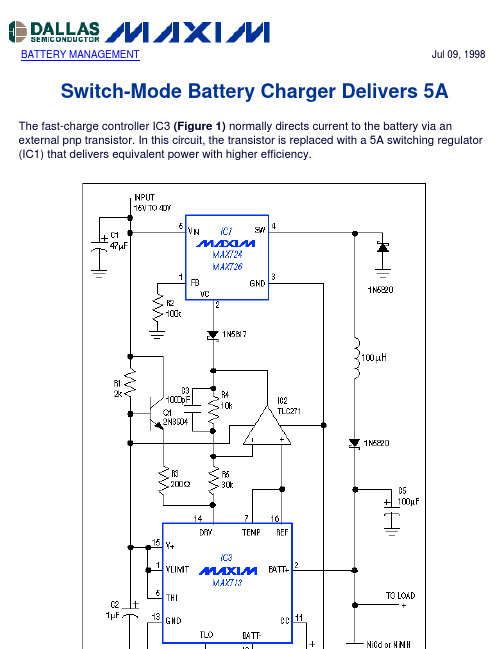
BATTERY MANAGEMENT Jul 09, 1998 Switch-Mode Battery Charger Delivers 5AThe fast-charge controller IC3 (Figure 1) normally directs current to the battery via an external pnp transistor. In this circuit, the transistor is replaced with a 5A switching regulator (IC1) that delivers equivalent power with higher efficiency.Figure 1. By controlling the PWM duty cycle of switching regulator IC1, the fast-charge controller (IC3) makes efficient delivery of the battery's charging current.IC1 is a 5A buck switching regulator whose output is configured as a current source. Its internal power switch (an npn transistor) is relatively efficient because V CE(SAT) is small in comparison with the 15V-to-40V inputs. (For applications that require 2A or less, the low-saturation, non-Darlington power switch of a MAX726 offers better efficiency.)R6 senses the battery-charging current and enables IC3 to generate an analog drive signal at DRV. The signal is first attenuated by the op amp to assure stability by reducing gain in the control loop. It then drives IC1's compensation pin (VC), which gives direct access to the internal PWM comparator. IC3 thus controls the charging current via the PWM duty cycle of IC1. The Q1 buffer provides current to the DRV input.Loop stability is also determined by the feedback loop's dominant pole, set by C4 at the CC terminal of IC3. If you increase the value of the battery filter capacitor (C5), you should make a proportional increase in the value of C4. Lower values, however, assure good transient response. If your application produces load transients during the fast-charge cycle, check the worst-case response to a load step. To assure proper termination of the charge, battery voltage should settle within 2msec to 5mV times N (where N is the number of battery cells). More InformationMAX713:QuickView-- Full (PDF) Data Sheet-- Free Samples。
HL7133规格书xx

无负载
--
(除特殊注明以外:Ta=25℃)
最小 典型 最大 单位 测定
值
值
值
电路
1.455 1.5 1.545 V
1
10
mA
3
200
mV
0.05 0.2 %/V
负载稳定度
输出电压温度系 数
消耗电流 输入电压
VOUT IOUT Vdrop △VOUT1 △VIN·VOUT
△VOUT2
△VOUT △Ta·VOUT
ISS1 VIN
VIN= 5.3V,IOUT=10mA VIN= 5.3V
IOUT=1 mA 4.3V≤VIN≤15V
IOUT=1mA VIN=5.3V 1.0mA≤IOUT≤30mA VIN=5.3V,IOUT=10mA -40℃≤Ta≤85℃ VIN=15V
IOUT=1mA VIN=5.6V 1.0mA≤IOUT≤30mA VIN=5.6V,IOUT=10mA -40℃≤Ta≤85℃ VIN=15V
无负载
--
(除特殊注明以外:Ta=25℃)
最小 典型 最大 单位 测定
值
值
值
电路
3.492 3.6 3.708 V
1
30
mA
3
40
mV
1
0.05 0.2 %/V
■ 产品目录
型号
输出电压(注)
误差
H L7115
1.5V
H L7130
3.0V
H L7133
3.3V
H L7136
- 1、下载文档前请自行甄别文档内容的完整性,平台不提供额外的编辑、内容补充、找答案等附加服务。
- 2、"仅部分预览"的文档,不可在线预览部分如存在完整性等问题,可反馈申请退款(可完整预览的文档不适用该条件!)。
- 3、如文档侵犯您的权益,请联系客服反馈,我们会尽快为您处理(人工客服工作时间:9:00-18:30)。
TC1070/TC1071/TC1187
1.0 ELECTRICAL CHARACTERISTICS
† Notice: Stresses above those listed under "Absolute Maximum Ratings" may cause permanent damage to the device. These are stress ratings only and functional operation of the device at these or any other conditions above those indicated in the operation sections of the specifications is not implied. Exposure to Absolute Maximum Rating conditions for extended periods may affect device reliability.
Description:
The TC1070, TC1071 and TC1187 devices are adjustable LDOs designed to supersede a variety of older (bipolar) voltage regulators. Total supply current is typically 50 µA at full load (20 to 60 times lower than in bipolar regulators). The devices’ key features include ultra low-noise operation, very low dropout voltage – typically 85 mV (TC1070), 180 mV (TC1071) and 270 mV (TC1187) at full load and fast response to step changes in load. Supply current is reduced to 0.5 µA (maximum) when the shutdown input is low. The devices incorporate both overtemperature and overcurrent protection. Output voltage is programmed with a simple resistor divider from VOUT to ADJ to GND. The TC1070, TC1071 and TC1187 devices are stable with an output capacitor of only 1 µF and have a maximum output current of 50 mA, 100 mA and 150 mA, respectively. For higher output versions please see the TC1174 (IOUT = 300 mA) data sheet (DS21363).
Typical Application
VIN 1 VIN VOUT 5 C1 + 1 µF R1 VOUT
Package Type
5-Pin SOT-23 VOUT 5 TC1070 TC1071 TC1187
R2
TC1070 TC1071 TC1187 2 GND
ADJ 4
3
SHDN
Байду номын сангаасADJ
4
1 VIN
2
3
GND SHDN
Shutdown Control (from Power Control Logic)
R1 V OUT = V REF ------+1 R2
2010 Microchip Technology Inc.
DS21353E-page 1
芯天下--/
2:
3: 4:
5:
6:
DS21353E-page 2
2010 Microchip Technology Inc.
芯天下--/
TC1070/TC1071/TC1187
ELECTRICAL SPECIFICATIONS (CONTINUED)
Electrical Characteristics: VIN = VOUT + 1V, IL = 0.1 mA, CL = 3.3 µF, SHDN > VIH, TA = +25°C, unless otherwise noted. Boldface type specifications apply for junction temperatures of -40°C to +125°C. Parameter Dropout Voltage (Note 3) Symbol VIN-VOUT Min — — — — — Supply Current Shutdown Supply Current Power Supply Rejection Ratio Output Short Circuit Current Thermal Regulation Thermal Shutdown Die Temperature Thermal Shutdown Hysteresis Output Noise SHDN Input SHDN Input High Threshold SHDN Input Low Threshold ADJ Input Adjust Input Leakage Current Note 1: IADJ — 50 — pA VIH VIL 45 — — — — 15 %VIN %VIN VIN = 2.5V to 6.5V VIN = 2.5V to 6.5V IIN IINSD PSRR IOUTSC VOUT/PD TSD TSD eN — — — — — — — — Typ 2 65 85 180 270 50 0.05 64 300 0.04 160 10 260 Max — — 120 250 400 80 0.5 — 450 — — — — µA µA dB mA V/W °C °C nV/Hz IL = IOUTmax Units mV Test Conditions IL = 0.1 mA IL = 20 mA IL = 50 mA TC1071, TC1187 IL = 100 mA TC1187 IL = 150 mA SHDN = VIH, IL = 0 SHDN = 0V FRE1 kHz VOUT = 0V Note 4
Absolute Maximum Ratings†
Input Voltage .........................................................6.5V Output Voltage........................... (-0.3V) to (VIN + 0.3V) Power Dissipation................Internally Limited (Note 5) Maximum Voltage on Any Pin ........VIN +0.3V to -0.3V Operating Temperature Range...... -40°C < TJ < 125°C Storage Temperature..........................-65°C to +150°C
TC1070/TC1071/TC1187
50 mA, 100 mA and 150 mA Adjustable CMOS LDOs with Shutdown
Features:
• • • • • • • • 50 µA Ground Current for Longer Battery Life Adjustable Output Voltage Very Low Dropout Voltage Choice of 50 mA (TC1070), 100 mA (TC1071) and 150 mA (TC1187) Output Power-Saving Shutdown mode Overcurrent and Overtemperature Protection Space-Saving 5-Pin SOT-23 Package Pin Compatible with Bipolar Regulators
Applications:
• • • • • • • Battery Operated Systems Portable Computers Medical Instruments Instrumentation Cellular/GSM/PHS Phones Linear Post-Regulators for SMPS Pagers
ELECTRICAL SPECIFICATIONS
Electrical Characteristics: VIN = VOUT + 1V, IL = 0.1 mA, CL = 3.3 µF, SHDN > VIH, TA = +25°C, unless otherwise noted. Boldface type specifications apply for junction temperatures of -40°C to +125°C. Parameter Input Operating Voltage Maximum Output Current Symbol VIN IOUTmax Min 2.7 50 100 150 Adjustable Output Voltage Range Reference Voltage VREF Temperature Coefficient Line Regulation Load Regulation (Note 2) VOUT VREF VREF/T VOUT/VIN VOUT/VOUT VREF 1.165 — — — — Note 1: TC VOUT = (VOUTmax – VOUTMIN) x 106 VOUTx T Regulation is measured at a constant junction temperature using low duty cycle pulse testing. Load regulation is tested over a load range from 0.1 mA to the maximum specified output current. Changes in output voltage due to heating effects are covered by the thermal regulation specification. Dropout voltage is defined as the input to output differential at which the output voltage drops 2% below its nominal value. Thermal Regulation is defined as the change in output voltage at a time T after a change in power dissipation is applied, excluding load or line regulation effects. Specifications are for a current pulse equal to Ilmax at VIN = 6V for T = 10 ms. The maximum allowable power dissipation is a function of ambient temperature, the maximum allowable junction temperature and the thermal resistance from junction-to-air (i.e., Ta, Tj, ja). Exceeding the maximum allowable power dissipation causes the device to initiate thermal shutdown. Please see Section 5.0 “Thermal Considerations” for more details. The minimum VIN has to justify the conditions: VIN VR + VDROPOUT and VIN 2.7V for IL = 0.1 mA to IOUTMAX. Typ — — — — — 1.20 40 0.05 0.5 0.5 Max 6.0 — — — 5.5 1.235 — 0.35 2 3 V V ppm/°C % % Note 1 (VR + 1V) VIN6V TC1070, TC1071 IL = 0.1 mA to IOUTmax TC1187 IL = 0.1 mA to IOUTmax Units V mA Test Conditions Note 6 TC1070 TC1071 TC1187