F2UGRTB01BAUBC中文资料
B2001RU中文资料

Key Features:• 20W Output Power • 4:1 Input Voltage Range • Compact 1 x 2 Inch Case • 1,600 VDC Isolation • High Effi ciency • Single & Dual Outputs • Remote ON/OFF•Industry Standard Pin-Out B2000RU 4:1 Input Range, 20W Single & Dual Output DC/DC Con v ert e rsSeriesMicroPower Direct292 Page Street Suite DStoughton, MA 02072USAT: (781) 344-8226F: (781) 344-8481E: sales@ W: Electrical Specifi cationsSpecifi cations typical @ +25°C, nominal input voltage & rated output current, unless otherwise noted. Specifi cations subject to change without notice.Notes:1. Transient recovery is measured to within a 1% error band for a load step change of 75% to 50% to 25%.2. Operation at no-load will not damage these units. However, they may not meet all specifi cations.3. Dual output units may be connected to provide a 10 VDC, 24 VDC or 30 VDC output. To do this, connect the load across the positive (+Vout) and negative (-Vout) outputs and fl oat the output common.4. It is recommended that a fuse be used on the input of a power supply for protection. See the table above for the correct rating.To help meet EN55022 conducted emissions requirements, a simple Pi fi lter should be added externally to the input of the converter. Recommended components (C 1, C 2 & L 1) are shown in the diagram above.These compo-nents should be mounted as close to the module as possible.To meet the requiremets of EN61000-4-4, EN61000-4-5 and EN61000-4-6, an external capacitor is required. It is recommended that the value shown in the fi gure above (C 3) be used.When measuring output ripple, it is recommended that an external 1.0 µF ceramic capacitor be placed from the +Vout pin to the -Vout pin for single output units and from each output to common for dual output units. For noise sensitive applications, the use of 3.3 µF capacitors (as shown in the diagram above) will reduce the output ripple.A positive logic Remote On/Off input (Pin 6) can be usedto control the converter. An open collector (or open drain) switch (Q 1) is placed between the control input (Pin 6) and the -V Input (Pin 2).If not being used, the control input should be left open.Model Selection GuideRecommended Input/Output ComponentsPage 2 Web: • Email: sales@ • Tel: (781) 344 - 8226 • Fax: (781) 344 - 8481SeriesB2000RUA simple external circuit may be used to adjust Vout on single output models. To adjust the output DOWN, con-nect a 5%, 3W resistor between the plus output pin and the Vout trim pin. To adjust the output UP , connect a 5%, 3W resistor between the minus output pin and the Vout trim pin. Resistor values are given in the chart below. For UP/Down trimming capability, connect a 10 kW poten-tiometer between the plus and minus outputs with the wiper arm connected to the Vout trim pin.Care should be taken that the maximum output power of the unit does not exceed the maximum rating.Output Trim (Single Output Models)MicroPowerDirectWeb: • Email: sales@ • Tel: (781) 344 - 8226 • Fax: (781) 344 - 8481Page 3MicroPower Direct292 Page Street Ste D Stoughton, MA 02072 • TEL: (781) 344-8226 • FAX: (781) 344-8481 • E-Mail: sales@Mechanical DimensionsMechanical Notes:• All dimensions are typical in inch e s (mm)•Tolerance x.xx = ±0.01 (±0.25)Derating Curve。
RT9013B 1 DS9013B-02 产品说明书

1DS9013B-02 April 2011Pin ConfigurationsApplicationsCDMA/GSM Cellular Handsets Portable Information AppliancesLaptop, Palmtops, Notebook Computers Hand-Held InstrumentsMini PCI & PCI-Express Cards PCMCIA & New Cards300mA, Low Dropout, Low Noise Ultra-Fast Without Bypass Capacitor CMOS LDO RegulatorOrdering InformationGeneral DescriptionThe RT9013B is a high-performance, 300mA LDO regulator,offering extremely high PSRR and ultra-low dropout. The RT9013B is Ideal for portable RF and wireless applications with demanding performance and space requirements.The RT9013B provides quiescent current to be as low as 25uA to extend the battery life. The RT9013B also works with low-ESR ceramic capacitors, reducing the amount of board space necessary for power applications, especially for hand-held wireless devices.The RT9013B consumes typical 0.7uA in shutdown mode and has fast turn-on time to be less than 40us. The other features include ultra-low dropout voltage, high output accuracy, current limiting protection, and high ripple rejection ratio. The RT9013B is available in the SC-70-5and WDFN-6L 1.6x1.6 packages.(TOP VIEW)FeaturesWide Operating Voltage Range : 2.2V to 5.5V Low Dropout : 150mV at 300mA Ultra-Low-Noise for RF ApplicationUltra-Fast in Line/Load Transient Response Current Limiting Protection Thermal Shutdown ProtectionHigh Power Supply Rejection RatioOnly 1uF Output Capacitor Required for Stability TTL-Logic-Controlled Shutdown InputRoHS Compliant and 100% Lead (Pb)-FreeSC-70-5Note :Richtek products are :` RoHS compliant and compatible with the current require-ments of IPC/JEDEC J-STD-020.` Suitable for use in SnPb or Pb-free soldering processes.Marking InformationFor marking information, contact our sales representative directly or through a Richtek distributor located in your area.WDFN-6L 1.6x1.6EN VINNC VOUTNC GNDRT9013B 12 : 1.2V 13 : 1.3V :34 : 3.4V 35 : 3.5V 1B : 1.25V 1H : 1.85V 2H : 2.85V2DS9013B-02 April 2011 Typical Application CircuitFunctional Pin DescriptionFunction Block DiagramENVINV OUT3DS9013B-02 April 2011Absolute Maximum Ratings (Note 1)Supply Input Voltage ------------------------------------------------------------------------------------------------------6V EN Input Voltage -----------------------------------------------------------------------------------------------------------6VPower Dissipation, P D @ T A = 25°CSC-70-5----------------------------------------------------------------------------------------------------------------------0.3W WDFN-6L 1.6x1.6---------------------------------------------------------------------------------------------------------0.606WPackage Thermal Resistance (Note 2)SC-70-5, θJA ----------------------------------------------------------------------------------------------------------------333°C/W WDFN-6L 1.6x1.6, θJA ----------------------------------------------------------------------------------------------------165°C/W Lead Temperature (Soldering, 10 sec.)-------------------------------------------------------------------------------260°C Junction T emperature -----------------------------------------------------------------------------------------------------150°CStorage T emperature Range --------------------------------------------------------------------------------------------−65°C to 150°CESD Susceptibility (Note 3)HBM --------------------------------------------------------------------------------------------------------------------------2kV MM ----------------------------------------------------------------------------------------------------------------------------200VRecommended Operating Conditions (Note 4)Supply Input Voltage ------------------------------------------------------------------------------------------------------2.2V to 5.5V Junction T emperature Range -------------------------------------------------------------------------------------------- −40°C to 125°CAmbient T emperature Range -------------------------------------------------------------------------------------------- −40°C to 85°CElectrical Characteristics(V IN = V OUT + 0.5V, V EN = V IN , C IN = C OUT = 1uF/X7R (Ceramic), T A = 25°C, unless otherwise specified)4DS9013B-02 April 2011 Note 1. Stresses listed as the above “Absolute Maximum Ratings ” may cause permanent damage to the device. These are forstress ratings. Functional operation of the device at these or any other conditions beyond those indicated in the operational sections of the specifications is not implied. Exposure to absolute maximum rating conditions for extended periods may remain possibility to affect device reliability.Note 2. θJA is measured in the natural convection at T A = 25°C on a low effective thermal conductivity single layer test board ofJEDEC 51-3 thermal measurement standard.Note 3. Devices are ESD sensitive. Handling precaution is recommended.Note 4. The device is not guaranteed to function outside its operating conditions.Note 5. Quiescent, or ground current, is the difference between input and output currents. It is defined by I Q = I IN - I OUT under noload condition (I OUT = 0mA). The total current drawn from the supply is the sum of the load current plus the ground pin current.Note 6. The dropout voltage is defined as V IN -V OUT , which is measured when V OUT is V OUT(NORMAL) - 100mV.Note 7. Regulation is measured at constant junction temperature by using a 2ms current pulse. Devices are tested for loadregulation in the load range from 10mA to 300mA.5DS9013B-02 April 2011Typical Operating CharacteristicsOutput Voltage vs. Temperature1.401.421.441.461.481.501.521.541.561.581.60-50-25255075100125Temperature O u t p u t V o l t a g e (V )(°C)(C IN = C OUT = 1μ/X7R, unless otherwise specified)Quiescent Current vs. Temperature1012141618202224262830-50-250255075100125Temperature Q u i e s c e n t C u r r e n t (u A )(°C)V IN = 2.5V, I LOAD = 50mA EN Pin Shutdown ResponseE N P i n V o l t a g e (V )Time (100μs/Div)O u t p u t V o l t a g e (V )420210RT9013B-15PU5V IN = 2.5V, I LOAD = 75mA Start UpTime (5μs/Div)E N P i n V o l t a g e (V )O u t p u t V o l t a g e (V )4201.00.50RT9013B-15PU5V IN = 2.6V to 3.6V, I LOAD = 10mAI n p u t V o l t a g e D e v i a t i o n (V )Time (100μs/Div)O u t p u t V o l t a g e D e v i a t i o n (m V )3.62.6200-20RT9013B-15PU5Dropout Voltage vs. Load Current020406080100120140160180200050100150200250300Load Current (mA)D r o p o u t V o l t a g e (m V )6DS9013B-02 April 2011 V IN = 2.5V, I LOAD= 10mA to 100mAL o a d C u r r e n t (m A )Time (100μs/Div)O u t p u t V o l t a ge D e v i a t i on (m V )100500500-50RT9013B-15PU5V IN = 3.0V (By Battery), No Load NoiseTime (10ms/Div)RT9013B-15PU5Time (10ms/Div)I n p u t V o l t a g e D e v i a t i o n (V )Time (100μs/Div)O u t p u t V o l t a g e D e v i a t i o n (m V )3.62.6200-20V IN = 2.6V to 3.6V, I LOAD = 100mART9013B-15PU5PSRR-70-60-50-40-30-20-1001020101001000100001000001000000Frequency (Hz)P S R R (d B )7DS9013B-02 April 2011Applications InformationLike any low-dropout regulator, the external capacitors used with the RT9013B must be carefully selected for regulator stability and performance. Using a capacitor whose value is > 1uF / X7R on the RT9013B input and the amount of capacitance can be increased without limit. The input capacitor must be located at a distance of not more than 0.5 inch from the input pin of the IC and returned to a clean analog ground. Any good quality ceramic can be used for this capacitor. The capacitor with larger value and lower ESR (equivalent series resistance) provides better PSRR and line-transient response.The output capacitor must meet both requirements for minimum amount of capacitance and ESR in all LDOs application. The RT9013B is designed specifically to work with low ESR ceramic output capacitor in space-saving and performance consideration. Using a ceramic capacitor whose value is at least 1uF with ESR is > 20m Ω on the RT9013B output ensures stability. The RT9013B still works well with output capacitor of other types due to the wide stable ESR range. Figure 1. shows the curves of allowable ESR range as a function of load current for various output capacitor values. Output capacitor of larger capacitance can reduce noise and improve load transient response,stability, and PSRR. The output capacitor should be located not more than 0.5 inch from the VOUT pin of the RT9013B and returned to a clean analog ground.⎟⎠⎞⎜⎝⎛×=ΔSupply Error ΔGain log 20 PSRR Figure 1EnableThe RT9013B goes into sleep mode when the EN pin is in a logic low condition. During this condition, the RT9013B has an EN pin to turn on or turn off the regulator, When the EN pin is logic hight the regulator will be turned on. The supply current to 0.7uA typical. The EN pin may be directly tied to V IN to keep the part on. The Enable input is CMOS logic and cannot be left floating.PSRRThe power supply rejection ratio (PSRR) is defined as the gain from the input to output divided by the gain from the supply to the output. The PSRR is found to beNote that in heavy load measuring, Δsupply will cause Δtemperature. And Δtemperature will cause Δoutput voltage. So the temperature effect is include in heavy load PSRR measuring.Current LimitThe RT9013B contains an independent current limiter, which monitors and controls the pass transistor's gate voltage,limiting the output current to 0.4A (typ.). The output can be shorted to ground indefinitely without damaging the part.Thermal Considerations°C,°C.°C. The − V OUT ) x I OUT + V IN x I QThe maximum power dissipation depends on the thermal resistance of IC package, PCB layout, the rate of surroundings airflow and temperature difference betweenRegion of Stable C OUT ESR vs. Load Current0.0010.010.111010050100150200250300Load Current (mA)R e g i o n o f S t a b l e C O U T E S R (Ω)R e g i o n o f S t a b l e C O U TE S R (Ω)8DS9013B-02 April 2011Figure 2. Derating Curves for RT9013B Packages00.10.20.30.40.50.60.70.80255075100125Ambient Temperature (°C)P o w e rD i s s i p a t i o n (W )junction to ambient. The maximum power dissipation can be calculated by following formula :P D(MAX) = ( T J(MAX) − T A ) /θJAWhere T J(MAX) is the maximum operation junction temperature, T A is the ambient temperature and the θJA is the junction to ambient thermal resistance.For recommended operating conditions specification of the RT9013B, where T J(MAX) is the maximum junction temperature of the die (125°C) and T A is the operated ambient temperature. The junction to ambient thermal resistance for SC-70-5 package is 333°C/W and WDFN-6L 1.6x1.6 package is 165°C/W on the standard JEDEC 51-3 single-layer thermal test board. The maximum power dissipation at T A = 25°C can be calculated by following formula :P D(MAX) = (125°C − 25°C) / (333°C/W) = 0.3W for SC-70-5packagesP D(MAX) = (125°C − 25°C) / (165°C/W) = 0.606W for WDFN-6L 1.6x1.6 packagesThe maximum power dissipation depends on operating ambient temperature for fixed T J(MAX) and thermal resistance θJA . For RT9013B packages, the Figure 2 of derating curves allows the designer to see the effect of rising ambient temperature on the maximum power allowed.(°C)9DS9013B-02 April 2011A1HLSC -70-5 Surface Mount PackageOutline Dimension10DS9013B-02 April 2011Information that is provided by Richtek Technology Corporation is believed to be accurate and reliable. Richtek reserves the right to make any change in circuit design,specification or other related things if necessary without notice at any time. No third party intellectual property infringement of the applications should be guaranteed by users when integrating Richtek products into any application. No legal responsibility for any said applications is assumed by Richtek.Richtek Technology CorporationHeadquarter5F, No. 20, Taiyuen Street, Chupei City Hsinchu, Taiwan, R.O.C.Tel: (8863)5526789 Fax: (8863)5526611Richtek Technology CorporationTaipei Office (Marketing)5F, No. 95, Minchiuan Road, Hsintien City Taipei County, Taiwan, R.O.C.Tel: (8862)86672399 Fax: (8862)86672377Email:*********************W-Type 6L DFN 1.6x1.6 Package。
常用二极管型号及全参数大全

1.塑封整流二极管序号型号 IF VRRM VF Trr 外形A V V μs1 1A1-1A7 1A 50-1000V 1.1 R-12 1N4001-1N4007 1A 50-1000V 1.1 DO-413 1N5391-1N5399 1.5A 50-1000V 1.1 DO-154 2A01-2A07 2A 50-1000V 1.0 DO-155 1N5400-1N5408 3A 50-1000V 0.95 DO-201AD6 6A05-6A10 6A 50-1000V 0.95 R-67 TS750-TS758 6A 50-800V 1.25 R-68 RL10-RL60 1A-6A 50-1000V 1.09 2CZ81-2CZ87 0.05A-3A 50-1000V 1.0 DO-4110 2CP21-2CP29 0.3A 100-1000V 1.0 DO-4111 2DZ14-2DZ15 0.5A-1A 200-1000V 1.0 DO-4112 2DP3-2DP5 0.3A-1A 200-1000V 1.0 DO-4113 BYW27 1A 200-1300V 1.0 DO-4114 DR202-DR210 2A 200-1000V 1.0 DO-1515 BY251-BY254 3A 200-800V 1.1 DO-201AD16 BY550-200~1000 5A 200-1000V 1.1 R-517 PX10A02-PX10A13 10A 200-1300V 1.1 PX18 PX12A02-PX12A13 12A 200-1300V 1.1 PX19 PX15A02-PX15A13 15A 200-1300V 1.1 PX20 ERA15-02~13 1A 200-1300V 1.0 R-121 ERB12-02~13 1A 200-1300V 1.0 DO-1522 ERC05-02~13 1.2A 200-1300V 1.0 DO-1523 ERC04-02~13 1.5A 200-1300V 1.0 DO-1524 ERD03-02~13 3A 200-1300V 1.0 DO-201AD25 EM1-EM2 1A-1.2A 200-1000V 0.97 DO-1526 RM1Z-RM1C 1A 200-1000V 0.95 DO-1527 RM2Z-RM2C 1.2A 200-1000V 0.95 DO-1528 RM11Z-RM11C 1.5A 200-1000V 0.95 DO-1529 RM3Z-RM3C 2.5A 200-1000V 0.97 DO-201AD30 RM4Z-RM4C 3A 200-1000V 0.97 DO-201AD2.快恢复塑封整流二极管序号型号 IF VRRM VF Trr 外形A V V μs(1)快恢复塑封整流二极管1 1F1-1F7 1A 50-1000V 1.3 0.15-0.5 R-12 FR10-FR60 1A-6A 50-1000V 1.3 0.15-0.53 1N4933-1N4937 1A 50-600V 1.2 0.2 DO-414 1N4942-1N4948 1A 200-1000V 1.3 0.15-0.5 DO-415 BA157-BA159 1A 400-1000V 1.3 0.15-0.25 DO-416 MR850-MR858 3A 100-800V 1.3 0.2 DO-201AD7 EU1-EU2 0.25A-1A 100-1000V 1.3 0.4 DO-418 20DF1-20DF10 2A 100-1000V 1.3 0.2 DO-159 30DF1-30DF10 3A 100-1000V 1.3 0.2 DO-201AD10 RU1-RU4 0.25A-3A 100-1000V 1.3 0.411 ERA22-02~10 0.5A 200-1000V 1.3 0.4 R-112 ERA18-02~10 0.8A 200-1000V 1.3 0.4 R-113 ERB43-02~10 0.5A 200-1000V 1.3 0.4 DO-4114 ERB44-02~10 1A 200-1000V 1.3 0.4 DO-1515 ERC18-02~10 1.2A 200-1000V 1.3 0.4 DO-1516 ERD28-02~10 1.5A 200-1000V 1.3 0.4 DO-201AD17 ERD29-02~10 2.5A 200-1000V 1.3 0.4 DO-201AD18 ERD32-02~10 3A 200-1000V 1.3 0.4 DO-201AD19 ERD09-13~15 3A 1300-1500V 1.5 0.6 R-5(2)SK、2CG系列快恢复整流二极管1 SK1-02~30 1.5A 200-3000V 1.3-4 0.5-1 DO-152 SK2-02~30 1A 200-3000V 1.3-4 0.5-1 DO-413 SK3-02~30 2A 200-3000V 1.3-4 0.5-1 DO-154 SK4-02~30 0.5A 300-3000V 1.3-4 0.5-1 DO-415 2CG04-2CG30 0.2A 300-3000V 1.3-4 0.5-1 DO-41 (3)快恢复塑封阻尼二极管1 2CN1-2CN1C 1A 200-1200V 1.32 DO-412 2CN2D-2CN2M 0.5A 200-1000V 1.3 2 DO-413 2CN3D-2CN3M 1A 200-1000V 1.3 6 DO-414 2CN4D-2CN4M 1.5A 200-1000V 1.3 0.8 DO-155 2CN5D-2CN5M 1.5A 200-1000V 1.0 1 DO-156 2CN6D-2CN6M 1A 200-1000V 1.3 6 DO-417 2CN12D-2CN12M 3A 200-1000V 1.3 1 DO-201AD8 RH1Z-RH1C 0.6A 200-1000V 1.3 4 DO-419 TVR4J-TVR4N 1.2A 600-1000V 1.2 20 DO-153.超高频塑封二极管1 ERA34-10 0.1A 1000V 3 0.15 R-12 ERA32-02~10 1A 200-1000V 1.3 0.1 DO-413 ERB32-02~10 1.2A 200-1000V 1.3 0.1 DO-154 ERC30-02~10 1.5A 200-1000V 1.3 0.1 DO-155 ERC32-02~10 3A 200-1000V 1.3 0.1 DO-201AD6 EG01E-EG01C 0.5A 200-1000V 2 0.1 DO-417 EG1E-EG1C 1A 200-1000V 1.8 0.1 DO-418 RG10Z-RG10C 1.2A 200-1000V 2 0.1 DO-159 RG2Z-RG2C 1.5A 200-1000V 1.8 0.1 DO-1510 RG4Z-RG4C 3A 200-1000V 2 0.1 D0-201AD4.超快恢复塑封二极管序号型号 IF VRRM VF Trr 外形A V V ns(1)超快恢复塑封二极管1 SF10-SF50 1-5A 50-1000V 0.95-1.7 352 SF80-SF160 8-16A 50-600V 0.95-1.4 35 TO-2203 EGP10-EGP50 1-5A 50-200V 1.1 354 ERC38~04-ERC38~10 1A 400-1000V 1.7 50 DO-415 RL2-RL2C 2A 400-1000V 1.7 50 DO-156 RL3-RL3C 3A 400-1000V 1.7 50 DO-201AD7 1H1-1H8 1A 50-1000V 1.1-1.7 50-75 R-18 HER10-HER60 1-6A 50-1000V 1.1-1.7 50-759 HER80-HER160 8-6A 50-1000V 1.1-1.7 50-75 TO-22010 UF10-UF60 1-6A 50-1000V 1.1-1.7 50-7511 EL1Z-EL1 1.5A 200-350V 1.3 50 DO-15(2)MUR超快恢复整流二极管1 MUR120-MUR1120 1A 200-1200V 0.95-1.5 35-50 DO-412 MUR420-MUR4120 4A 200-1200V 0.95-1.6 35-75 DO-201AD3 MUR820-MUR8120 8A 200-1200V 1.3-2.1 35-75 TO-220AC4 MUR1020-MUR10120 10A 200-1200V 1.3-2.1 35-75 TO-220AC5 MUR1520-MUR15120 15A 200-1200V 1.3-2.1 35-75 TO-220AC6 MUR2020-MUR20120 20A 200-1200V 1.3-2.1 35-75 TO-220AB7 MUR3020-MUR30120 30A 200-1200V 1.3-2.1 35-75 TO-247AD8 MUR6020-MUR60120 60A 200-1200V 1.3-2.1 35-75 TO-247AD (3)RHRP、RHRG超快恢复二极管1 RHRP820-RHRP8120 8A 200-1200V 2.1-3.2 35-70 TO-220AC2 RHRP1520-RHRP15120 15A 200-1200V 2.1-3.2 40-75 TO-220AC3 RHRP3020-RHRP30120 30A 200-1200V 2.1-3.2 45-75 TO-220AC4 RHRG3020-RHRG30120 30A 200-1200V 2.1-3.2 45-75 TO-247AC5 RHRG5020-RHRG50120 50A 200-1200V 2.1-3.2 50-100 TO-247AC6 RHRG6020-RHRG60120 60A 200-1200V 2.1-3.2 45-75 TO-247AD (4)BYV29~79、BYT28~79超快恢复二极管1 BYW29-100~200 8A 100-200V 1.1 25 TO-220AC2 BYV29-300~500 9A 300-500V 1.25 60 TO-220AC3 BYQ28 -100~200 10A 100-200V 1.1 20 TO-220AB4 BYT28-300~500 10A 300-500V 1.4 60 TO-220AB5 BYV79-100~200 14A 100-200V 1.3 30 TO-220AC6 BYT79-300~500 14A 300-500V 1.4 60 TO-220AC7 BYV32-100~200 20A 100-200V 1.1 25 TO-220AB8 BYV34-300~500 20A 300-500V 1.1 60 TO-220AB9 BYV42-100~200 30A 100-200V 1.1 28 TO-220AB10 BYV44-300~500 30A 300-500V 1.25 60 TO-220AB5.肖特基整流二极管序号型号 IF VRRM VF 外形A V V(1)肖特基塑封整流二极管1 1N5817-1N5819 1A 20-40V 0.45-0.6 DO-412 1N5820-1N5822 3A 20-40V 0.45-0.6 DO-201AD3 SRT12-SRT100 1A 20-100V 0.55-0.85 R-14 SR10-SR50 1-5A 20-100V 0.55-0.855 SB120-SB1B0 1A 20-100V 0.55-0.85 DO-416 SB220-SB2B0 2A 20-100V 0.55-0.85 DO-157 SB320-SB3B0 3A 20-100V 0.55-0.85 DO-201AD8 SB520-SB5B0 5A 20-100V 0.55-0.85 D0-201AD9 ERA81-002~009 1A 20-90V 0.55-0.9 DO-4110 ERB81-002~009 2A 20-90V 0.55-0.9 DO-1511 ERC81-002~009 3A 20-90V 0.55-0.9 DO201AD12 EK03-EK09 1A 20-90V 0.55-0.81 DO-4113 EK13-EK19 1.5A 20-90V 0.55-0.81 DO-1514 EK33-EK39 2A 20-90V 0.55-0.81 DO-1515 EK43-EK49 3A 20-90V 0.55-0.81 DO-201AD(2)MBR、PBYR系列大电流肖特基整流二极管1 MBR1020-MBR1060 10A 20-60V 0.57-0.8 TO-220AC2 MBR1620-MBR1660 16A 20-60V 0.57-0.8 TO-220AC3 MBR2020CT-2060CT 20A 20-60V 0.57-0.8 TO-220AB4 MBR2520CT-2560CT 25A 20-60V 0.57-0.8 TO-220AB5 MBR3020PT-3060PT 30A 20-60V 0.57-0.8 TO-247AD6 MBR4020PT-4060PT 40A 20-60V 0.57-0.8 TO-247AD7 MBR6020PT-6060PT 60A 20-60V 0.57-0.8 TO-247AD8 PBYR735-745 7A 20-45V 0.56-0.66 TO-220AC9 PBYR1020-1060 10A 20-60V 0.56-0.77 TO-220AC10 PBYR1635-1660 16A 20-60V 0.56-0.77 TO-220AC11 PBYR2020CT-2045CT 20A 20-45V 0.56-0.65 TO-220AB12 PBYR3035PT-3060PT 30A 20-60V 0.56-0.77 TO-247AD 6.玻球快恢复二极管、玻钝芯片塑封二极管序号型号 IF VRRM VF Trr 外形A V V ns(1)BYV、BYT、BYM、BYW玻球快恢复二极管1 BYV26A-BYV26E 1A 200-1000V 1.5 0.03 DO-204AP2 BYV12-BYV16 1.5A 100-1000V 1.5 0.3 DO-204AP3 BYV96A-BYV96E 1.5A 100-1000V 1.5 0.3 DO-204AP4 BYV27-50~200 2A 50-200V 1.1 0.025 DO-204AP5 BYV28-50~200 3.5A 50-200V 1.1 0.03 G36 BYT52A-BYT52M 1A 50-1000V 1.3 0.2 DO-204AP7 BYT54A-BYT54M 1.25A 50-1000V 1.5 0.1 DO-204AP8 BYT53A-BYT53M 1.5A 50-1000V 1.1 0.05 DO-204AP9 BYT56A-BYT56M 3A 200-1000V 1.4 0.1 G310 BYM26A-BYM26M 2.3A 200-1000V 1.5 0.03 G311 BYM36A-BYM36M 3A 200-1000V 1.1 0.15 G312 BYW32-BYW38 2A 200-1000V 1.1 0.2 DO-204AP13 BYW52-BYW56 2A 200-1000V 1.1 4 DO-204AP14 BYW72-BYW76 3A 200-600V 1.1 0.2 G315 BYW96A-BYW96E 3A 200-1000V 1.5 0.2 G316 BY228 3A 1500V 1.5 20 G3(2)GP、RGP系列玻钝芯片塑封二极管17 GP10-GP30 1-3A 50-1000V 1.118 RGP01-10~RGP01-20 0.1A 1000-2000V 2 0.2-0.5 DO-4119 RGP05-10~RGP05-20 0.5A 1000-2000V 2 0.2-0.5 DO-4120 RGP10-RGP60 1-6A 50-2000V 1.3 0.15-0.57.PD、TR、PR系列高压塑封二极管1 PD0112-PD0160 0.1A 1200-6000V 1.2-5 DO-412 PD0312-PD0360 0.3A 1200-6000V 1.2-5 DO-153 PD0512-PD0560 0.5A 1200-6000V 1.2-5 DO-154 PD112-PD130 1A 1200-3000V 1.2-4 DO-155 PD1512-PD1530 1.5A 1200-3000V 1.2-4 DO-156 PD212-PD220 2A 1200-2000V 1.2-2.5 DO-201AD7 PD312-PD320 3A 1200-2000V 1.2-2.5 DO-201AD8 PD612-PD620 6A 1200-2000V 1.2-2.5 R-69 TR0112-TR0160 0.1A 1200-6000V 1.5-8 0.5-0.8 DO-4110 TR0312-TR0360 0.3A 1200-6000V 1.5-8 0.5-0.8 DO-1511 TR0512-TR0560 0.5A 1200-6000V 1.5-8 0.5-0.8 DO-1512 TR112-TR130 1A 1200-3000V 1.5-6 0.5-0.8 DO-1513 TR1512-TR1530 1.5A 1200-3000V 1.5-6 0.5-0.8 DO-1514 TR212-TR220 2A 1200-2000V 1.5-2.7 0.5-0.8 DO-201AD15 TR312-TR320 3A 1200-2000V 1.5-2.7 0.5-0.7 DO-201AD16 TR612-TR620 6A 1200-2000V 1.5-2.7 0.5-0.8 R-617 PR01-PR1 0.1-1A 1200-3000V 1.5-4 0.1-0.5 DO-1518 RC2 0.3A 2000V 3 0.5 DO-4119 RU4D-RP3F 1.5A-2A 1300-1500V 1.5 0.3 DO-201AD8.稳压二极管序号名称型号 PZM VZW V稳压二极管1 BZX55 0.5W 2.4V-47V2 1N5985B~1N6031B 0.5W 2.4V-200V3 1N4728~1N4764 1W 3.3V-100V4 1N5911B~1N5956B 1.5W 2.7V-200V5 2CW37-2.4~36 0.5W 2.4V-36V6 2CW51-2CW68 0.25W 3V-28.5V7 2CW101-2CW121 1W 3V-37.5V8 2DW50-2DW64 1W 41V-190V9 2DW80-2DW190 3W 41V-190V10 2DW110-2DW151 10W 4.3V-470V11 2DW170-2DW202 50W 4.3V-200V12 温度补偿稳压二极管 2DW230-2DW236 0.2W 5.8V-6.6V9.高速开关二极管序号型号 IC VRM Trr 外形mA V ns1 1N4148 150 100V 4 DO-352 1N4149-1N4154 150 35-100V 2-4 DO-353 1N4446-1N4454 150 40-100V 1-4 DO-354 1N914 75 100V 4 DO-355 BAV17-BAV21 250 25-250V 50 DO-356 BAW75-BAW76 300 35-75V 4 DO-357 2CK70-2CK79 10-280 20-60V 3-10 DO-358 2CK80-2CK85 10-300 20-60V 5-10 DO-359 1S1553-1S1555 100 70-35V 3 DO-3510 1S2471-1S2473 130-110 90-40V 3 DO-35几种常用二极管的特点1.整流二极管整流二极管结构主要是平面接触型,其特点是允许通过的电流比较大,反向击穿电压比较高,但PN结电容比较大,一般广泛应用于处理频率不高的电路中。
D2025UK中文资料

Document Number 5855 Issue 1
DIM A B C D E F G H
mm 26.16 5.72 45° 7.11 0.13 1.52 0.43 7.67
Tol. 0.38 0.13 5° 0.13 0.03 0.13 0.20 REF
Inches 1.030 0.225 45° 0.280 0.005 0.055 0.060 0.120
PD BVDSS BVGSS ID(sat) Tstg Tj Power Dissipation Drain – Source Breakdown Voltage Gate – Source Breakdown Voltage Drain Current Storage Temperature Maximum Operating Junction Temperature 17.5W 65V ±20V 1A –65 to 150°C 200°C
HAZARDOUS MATERIAL WARNING
The ceramic portion of the device between leads and metal flange is beryllium oxide. Beryllium oxide dust is highly toxic and care must be taken during handling and mounting to avoid damage to this area. THESE DEVICES MUST NEVER BE THROWN AWAY WITH GENERAL INDUSTRIAL OR DOMESTIC WASTE.
Typ.
Max. Unit
V 1 1 7 mA µA V S dB % — 12 6 0.5 pF pF pF
波士顿电器产品说明

36 1/2"–38" x 31 1/2" x 28 7/8"
Required cutout size (HxWxD)
35 1/2"–37" x 30" x 25"
Adjustable range height 1 1/2"
Oven cavity size
4.6 cu. ft.
Overall oven interior dimensions (HxWxD)
Warranties: Please see Use & Care manual or Bosch website for statement of limited warranty.
For more information on our entire line of products, go to /us or call 1-800-944-2904
General Properties
Cooking modes
Bake, Variable Broil (hi & low), Roast, Warm, Proof Dough, Convection Bake, Convection Broil, Convection Roast, Convection Multi-Rack, Convection Conversion, Pizza, Fast Preheat, Sabbath
for 7" element
HEZ390230 10" AutoChef® pan for 8" and 9" elements
Accessories: To purchase Bosch accessories, cleaners & parts please visit /us/store or call 1-800-944-2904 (Mon to Fri 5 am to 6 pm PST, Sat 6 am to 3 pm PST).
台电U盘工具
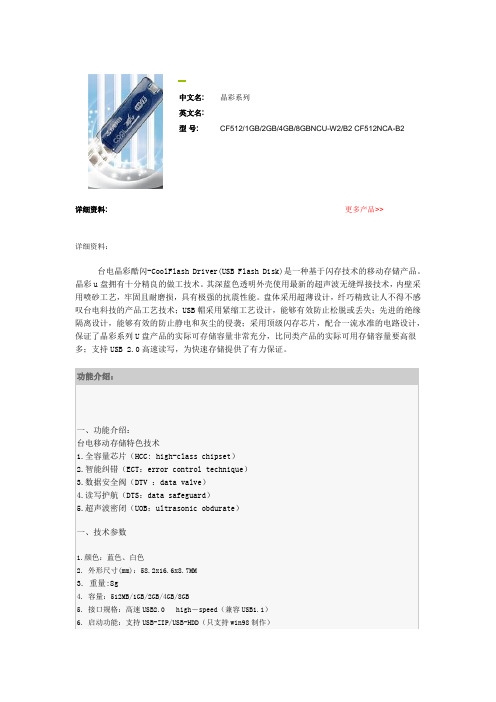
中文名:晶彩系列
英文名:
型号:CF512/1GB/2GB/4GB/8GBNCU-W2/B2 CF512NCA-B2
详细资料:更多产品>>
详细资料:
台电晶彩酷闪-CoolFlash Driver(USB Flash Disk)是一种基于闪存技术的移动存储产品。
晶彩u盘拥有十分精良的做工技术。
其深蓝色透明外壳使用最新的超声波无缝焊接技术,内壁采用喷砂工艺,牢固且耐磨损,具有极强的抗震性能。
盘体采用超薄设计,纤巧精致让人不得不感叹台电科技的产品工艺技术;USB帽采用紧缩工艺设计,能够有效防止松脱或丢失;先进的绝缘隔离设计,能够有效的防止静电和灰尘的侵袭;采用顶级闪存芯片,配合一流水准的电路设计,保证了晶彩系列U盘产品的实际可存储容量非常充分,比同类产品的实际可用存储容量要高很多;支持USB 2.0高速读写,为快速存储提供了有力保证。
晶彩(NCU)系列驱动程序
专用于晶彩NCU系列WIN98驱动程序及启动、分区、加密制作工具(支持Vista),适用于全系列(注:从包装彩盒右侧面型号贴纸上可查到产品名称)如:CF4GBNCU-B2
LOCK登入程序
此程序主要解决用户将LOCK程序删除后的解决方法,目前适用于欣喜(晶喜)系列、晶灵II代系列、晶彩系列、晶致系列、欣悦系列产品、晶灵III代系列
酷闪修复工具
此修复工具仅适合以下系列:晶彩系列、晶灵II代、天志系列、晶致系列、欣悦系列、欣喜(晶喜)系列、风尚系列、晶灵III代。
双基极二极管(精)

双基极二极管双基极二极管又称单结晶体管,具有两个基极,一个发射极的三端负阻器件,它具有频率易调、温度稳定性好等特点,用于张驰振荡电路,定时电压读出电路中。
双基极二极管又称单结晶体管,他有两个基极和一个发射极,如图(a)所示。
两个基极分别由Bl和B2表示,发射极用E表示。
图的(b)为双基极二极管的图形符号。
双基极二极管的参数中基极间电阻RBB是指发射极开路状态下,两个基极的电阻。
而分压比是指发射极E到基极由之间电压和基极B2到Bl之间的电压之比。
以上两个参数是双基极二极管的主要参数。
谷点电压Uv是表示双基极二极管由负阻区进人饱和区的分界点时,与其对应的发射区电压。
即双基极二极管赴于导通状态的最小电压值,如发射极电压UE低于谷点电压Uv,双基极二极管就进大了截止状态。
双基极二极管的主要参数(1)基极间电阻Rbb:发射极开路时,基极b1、b2之间的电阻,一般为2--10千欧,其数值随温度上升而增大。
(2)分压比η:由管子内部结构决定的常数,一般为0.3--0.85。
(3)eb1间反向电压Vcb1:b2开路,在额定反向电压Vcb2下,基极b1与发射极e之间的反向耐压。
(4)反向电流Ieo:b1开路,在额定反向电压Vcb2下,eb2间的反向电流。
(5)发射极饱和压降Veo:在最大发射极额定电流时,eb1间的压降。
(6)峰点电流Ip:单结晶体管刚开始导通时,发射极电压为峰点电压时的发射极电流。
双基极二极管(单结晶体管)的结构双基极二极管又称为单结晶体管,它的结构如图1所示。
在一片高电阻率的N型硅片一侧的两端各引出一个电极,分别称为第一基极B1和第二基极B2。
而在硅片是另一侧较靠近B2处制作一个PN结,在P型硅上引出一个电极,称为发射极E。
两个基极之间的电阻为R BB,一般在2~15k 之间,R BB一般可分为两段,R BB = R B1+ R B2,R B1是第一基极B1至PN结的电阻;R B2是第一基极B2至PN结的电阻。
分立元件库元件名称及中英对照

部分分立元件库元件名称及中英对照AND ------------------------------------与门ANTENNA --------------------------------天线BA TTERY --------------------------------直流电源BELL -----------------------------------铃,钟BVC ------------------------------------同轴电缆接插件BRIDEG 1 -------------------------------整流桥(二极管) BRIDEG 2 -------------------------------整流桥(集成块) BUFFER--------------------------------- 缓冲器BUZZER----------------------------------蜂鸣器CAP ------------------------------------电容CAPACITOR ------------------------------电容CAPACITOR POL --------------------------有极性电容CAPV AR ---------------------------------可调电容CIRCUIT BREAKER ------------------------熔断丝COAX -----------------------------------同轴电缆CON ------------------------------------插口CRYSTAL --------------------------------晶体整荡器DB --------------------------------------并行插口DIODE ---------------------------------二极管DIODE SCHOTTKY ------------------------稳压二极管DIODE V ARACTOR ------------------------变容二极管DPY_3-SEG---------------------------- 3段LEDDPY_7-SEG---------------------------- 7段LEDDPY_7-SEG_DP -------------------------7段LED(带小数点) ELECTRO ------------------------------电解电容FUSE ----------------------------------熔断器INDUCTOR -----------------------------电感INDUCTOR IRON -------------------------带铁芯电感INDUCTOR3 -----------------------------可调电感JFET N -------------------------------N沟道场效应管JFET P --------------------------------P沟道场效应管LAMP ----------------------------------灯泡LAMP NEDN -----------------------------起辉器LED -----------------------------------发光二极管METER ---------------------------------仪表MICROPHONE ----------------------------麦克风MOSFET --------------------------------MOS管MOTOR AC -----------------------------交流电机MOTOR SERVO --------------------------伺服电机NAND ----------------------------------与非门NOR ----------------------------------或非门NOT -----------------------------------非门NPN -----------------------------------NPN----三极管NPN-PHOTO ------------------------------感光三极管OPAMP ----------------------------------运放OR ------------------------------------或门PHOTO ---------------------------------感光二极管PNP -----------------------------------三极管NPN DAR ----------------------------NPN三极管PNP DAR ----------------------------PNP三极管POT ----------------------------滑线变阻器PELAY-DPDT---------------------------- 双刀双掷继电器RES1.2 ----------------------------电阻RES3.4 ----------------------------可变电阻RESISTOR BRIDGE ? ----------------------------桥式电阻RESPACK ? ----------------------------电阻SCR ----------------------------晶闸管PLUG ?---------------------------- 插头PLUG AC FEMALE---------------------------- 三相交流插头SOCKET ? ----------------------------插座SOURCE CURRENT---------------------------- 电流源SOURCE VOLTAGE ----------------------------电压源SPEAKER ----------------------------扬声器SW ? ----------------------------开关SW-DPDY ?---------------------------- 双刀双掷开关SW-SPST ? ----------------------------单刀单掷开关SW-PB ----------------------------按钮THERMISTOR ----------------------------电热调节器TRANS1 ----------------------------变压器TRANS2 ----------------------------可调变压器TRIAC ?---------------------------- 三端双向可控硅TRIODE ? ----------------------------三极真空管V ARISTOR ----------------------------变阻器ZENER ? ----------------------------齐纳二极管DPY_7-SEG_D---------------------------- 数码管SW-PB ---------------------------- 开关7805----------------------------------LM7805CT。
- 1、下载文档前请自行甄别文档内容的完整性,平台不提供额外的编辑、内容补充、找答案等附加服务。
- 2、"仅部分预览"的文档,不可在线预览部分如存在完整性等问题,可反馈申请退款(可完整预览的文档不适用该条件!)。
- 3、如文档侵犯您的权益,请联系客服反馈,我们会尽快为您处理(人工客服工作时间:9:00-18:30)。
PushbuttonFeatures/Benefits•Up to 10 poles per module •Various contact terminals •Various mounting & switchganging configurations•Mechanical indicator buttons •Illumination options •RoHS compliant Typical Applications •Audio selection•Digital equipment interface •Medical equipment interfaceSpecificationsSWITCHING POWER: F module max. AC/DC: Silver: 50 VA/15W,Gold: 1 VA/300 mW.SWITCHING VOLTAGE: F module max. AC/DC: Silver: 125/30V ,Gold: 50/30 V .SWITCHING CURRENT: F module max. AC/DC: Silver: 0.5A/0.5A,Gold: 0.04A/0.01A.CARRYING CURRENT: Max at d u = 20C: Silver: < 2A, Gold: <0.5A.DIELECTRIC STRENGTH (50 Hz, 1 min.): Chassis/contact: ^1500VBetween contacts: ^1500V .OPERATING LIFE “OA/EE” (24V/200mA): >105operations“GR”: >3.5 x 10⁴ operations.CONTACT RESISTANCE: Initial: Typical %10 m Ω, max. 20 m ΩAfter operating life: %100 m ΩINSULATION RESISTANCE: ^109Ωbetween open contacts,^109Ωbetween chassis and contacts.CAPACITANCE (at f = 10 kHz): %0.7 pF between 2 contacts.TOTAL TRAVEL/LATCHING TRAVEL: 4.7mm/3.3mm (.185 inch/.130 inch).All models and options are RoHS compliant and compatible.NOTE:For the latest information regarding RoHS compliance, please go to:/rohs. All models and options are RoHS compliant and compatible.NOTE:Specifications and materials listed above are for switches with standard options.For information on specific and custom switches, consult Customer Service Center.TYPICAL F OPERATING FORCE: 2U: 6.5N (650 grams); 4U: 6.5N(650 grams); 6U: 7.5N (750 grams); 8U: 9.0N (900 grams); 10U:9.0N (900 grams).EUROPEAN TYPICAL SF OPERATING FORCE:2U: 3.5N±0.5N (350 grams±100 grams); 4U: 5N±1N (500grams±100 grams); 6U: 6.5N±1N (650 grams±100 grams); 8U:9.0N±1N (900 grams±100 grams).OPERATING TEMPERATURE RANGE: -40˚C to 70˚C.MaterialsHOUSING: Polycarbonate UL 94V-0 or polyester UL 94V-0.ACTUATOR: Polyester UL 94V-0.MOVABLE CONTACTS: Bimetal brass, silver plated, gold plateover nickel.STATIONARY CONTACTS & TERMINALS: Brass, silver plated,gold plated.TERMINAL BOARD: Polyester UL 94V-0.RETURN SPRING: Music wire.TERMINAL SEAL: RTV adhesive sealant.CHASSIS: Steel.LOCKOUT PIN: Steel.BLOCKERS: Steel.Build-A-SwitchTo order, simply select desired option from each category and place in the appropriate box. Available options are shown and described on pages A-90 thru A-98. For additional options not shown in catalog, consult Customer Service Center. If requesting only a switch, select either a North American or European switch as noted below. Chassis and buttons are sold separately. If multiple stations are selected, we will assume all switches are the same unless noted otherwise.Designation F F SeriesFLT Light touch F series ZFCentral mounted F seriesTerminal Style(NONE)Solder lugs & PC pins 01A Cut solder lugs01B Cut PC pins,for other configurations,consult factoryElectrical Function (NONE)BBM M MBB (special)Contact Material (NONE)Silver,AG AU GoldDress nut**Central mounted F series only (NONE)No dress nut B Black C ChromeTerminal Sealing (NONE)None TB Top/bottomMechanical FunctionOA MomentaryEE Alternate (push-push)GR InterlockAOR Central releaseOASP Momentary with lockout GRSP Interlock with lockoutContact Arrangement 2U 2PDT4U 4PDT6U 6PDT8U BPDT10U 1OPDTNorth American Order Code - Switch OnlyP u s h b u t t o nDesignation SF F SeriesZFCentral mounted F seriesTerminal Style(NONE) Solder lugs &PC pinsLB Cut solder lugsPB Cut PC pins,for otherconfigurations,consult factory Electrical Function (NONE)BBMContact Material (NONE) Silver,AG P GoldDress nut**Central mounted F series only (NONE)No dress nut B Black C ChromeMechanical FunctionOA MomentaryEE Alternate (push-push)GR InterlockContact Arrangement 2U 2PDT4U 4PDT6U 6PDT8U BPDTStyle F01FMR F02FG*F12FSC F13FSD F14FU12F15FSB F16FE F19FA F21F001Button Color 01Black 02White 03Red04Light gray*Minimum order quantities apply.European Order Code - Switch OnlyOrder Code - ButtonsSolid ButtonsMechanical Indicator ButtonsStyleF01FA100F02FA101F07FA120F08FA2O1F11FA200*Shell Color 01BlackOut Position Color 01BlackIn Position Color 02White 06Yellow 07Blue 08Green 12Orange*Button options for central mounting configurations,use ‘FG’ for central mount with chrome dress nut,use ‘FA200’ for central mount with black dress nut.BUTTON REMOVALA button of a push-push switch should only be removed in the “OFF” non-latching position.PushbuttonSWITCHES WITH STANDARD OPTIONSOrder Code - ChassisT o order a switch with chassis, create the switch part number listed above and add the Chassis part number configurator information at the end of the part number.Note: We do not guarantee or recommend interlocking beyond 10 stations.No. of Stations01 thru 23Comes with standard.094 (2,4mm) mounting holesNote:Single station chassisavailable with special mountingconfigurations,consult factory.Spacing between Stations00Single station1010mm12.512.5mm1515mm17.517.5mm2020mmSpecial AcknowledgementsSee note*Minimum order quantities apply.2U0.827 (21,00)4U 1.300 (33,00)6U 1.770 (45,00)8U 2.240 (57,00)10U 2.720 (69,00)LENGTHDIM ‘L’CONTACTARRANGEMENT2U0.827 (21,00)4U 1.300 (33,00)6U 1.770 (45,00)8U 2.240 (57,00)10U 2.720 (69,00)LENGTHDIM ‘L’CONTACTARRANGEMENTZF2UEEBF11010108F2UEEPC MOUNTINGMomentary Alternate (push-push)InterlockOA EE GRFUNCTION OPTION CODEMomentary Alternate (push-push)Interlock Central release Momentary with lockout Interlock with lockoutOA EE GR AOR OASP GRSPFUNCTION OPTION CODENorth AmericaDesignation, North America F F SeriesFLT Light touch F series ZF Central mounted F seriesDesignation, Europe SF F SeriesZF Central mounted F seriesEuropeP u s h b u t t o nBBM Non-shortingMBB Shorting (North America only)(NONE) MFUNCTION OPTION CODEPushbuttonNOTE:For the latest information regarding RoHS compliance, please go to: /rohs.* Note: See Technical Data section of this catalog for RoHS compliant and compatible definitions and specifications.STYLEP u s h b u t t o nPushbuttonSTYLEP u s h b u t t o n.394(10,0).492(12,5)12.512.5mm1010mmC00 Thru C10Comes with standard 0.094 (2,44mm) mounting holesNOTE:Single station chassis available with mounting configurations, consult factory.NUMBER OF STATIONSSPACING00SINGLE STATION0.0154.567(116,00)4.331(110,01)100.0154.174(106,02)3.938(100,03)90.0153.780(96,01)3.544(90,02)80.0153.386(86,00)3.150(80,01)70.0152.993(76,02)2.757(70,03)60.0102.599(66,01)2.363(60,02)50.0102.205(56,01)1.969(50,01)40.0101.811(46,00)1.575(40,01)30.0051.418(36,02)1.182(30,02)2Tolerance Dim. ‘B’Dim. ‘A’No. of StationsPushbutton.591(15,0)SPACING0.0156.339(161,01)6.103(155,02)100.0155.749(146,02)5.513(140,03)90.0155.158(131,01)4.922(125,02)80.0154.568(116,03)4.332(110,03)70.0153.977(101,02)3.741(95,02)60.0103.386(86,00)3.150(80,01)50.0102.796(71,02)2.560(65,02)40.0102.205(56,01)1.969(50,01)30.0051.615(41,02)1.374(34,90)2Tolerance Dim. ‘B’Dim. ‘A’No. of Stations0.0157.225(183,52)6.989(177,52)100.0156.536(166,01)6.300(160,02)90.0155.847(148.51)5.611(142,52)80.0155.158(131,01)4.922(125,02)70.0154.469(113,51)4.233(107,52)60.0103.780(96,01)3.544(90,02)50.0103.091(78.51)2.855(75,52)40.0102.402(61,01)2.166(55,02)30.0051.713(43,51)1.477(37,52)2Tolerance Dim. ‘B’Dim. ‘A’No. of Stations0.0158.111(206,02)7.875(200,03)100.0157.323(186,00)7.087(180,01)90.0156.536(166,01)6.300(160,02)80.0155.748(146,00)5.512(140,00)70.0154.961(126,01)4.725(120,02)60.0104.174(106,02)3.938(100,03)50.0103.386(86,00)3.150(80,01)40.0102.599(66,01)2.363(60,02)30.0051.811(46,00)1.575(40,01)2Tolerance Dim. ‘B’Dim. ‘A’No. of Stations1515mm2020mm17.517.5mmP u s h b u t t o n。