M38232G7-XXXFP中文资料
LPC32x0技术文档(中文)doc-北京胜创特电子科技-3页word资料
208MHZ 32位ARM926EJ-S处理器这款先进的MCU采用强大的ARM926EJ-S内核,VFP协处理器,高效的内部总线矩阵和大量的标准外设来实现超强的性能主要特点:●支持主频为208MHz的ARM926EJ-S内核处理器带有ETM功能●矢量浮点协处理器(VFP)●使用90纳米的处理技术,在低电压模式下的工作电压可降到0.9V●256KB的内部SRAM和32kB指令高速缓存和32kB数据高速缓存●DDR,SDR和SDRAM以及静态设备的外部存储器控制器●可选择从不同的外设启动:NAND Flash、SPI、USB、UART或静态存储器●10/100以太网MAC带特定DMA控制器(仅用于LPC3240 &LPC3250)●USB 2.0全速device/Host /OTG控制器●24位LCD控制器带有专用的DMA控制器,支持STN和TFT●3通道10位的A/D 转换器带触摸屏接口●串行接口包括2个I2S,2个SPI,2个SSP,2个I2C总线和7个UART●SD存储卡接口●6个12位的定时器,看门狗定时器,11个PWM通道和带单独的电源管脚的实时时钟●8通道通用DMA控制●8 x 8键盘扫描接口和87个GPIO●具有RAM的仿真跟踪缓冲区,允许通过JTAG接口进行跟踪●工作温度范围:-40℃到+85℃●TFBGA296封装应用:●消费●医疗●工业●汽车制造●网络控制●通信功能特性:LPC32x0系列采用90纳米工艺设计,结合了ARM926EJ-S内核、一个矢量浮点协处理器(VFP)、LPC32x0的特点是高性能,高集成度和低功耗。
VFP协处理器在标量模式和最佳化向量模式下提高了标准运算的速度。
先进的加工技术完善了MCU的内部电源和软件控制特性,提供了卓越的电源管理系统。
LPC32x0包含了256kB的片内SRAM和外部存储器控制器,支持SDR,DDR SDRAM,SRAM,FLASH和静态设备。
M37548G3-XXXFP资料

Rev.2.00 Mar 15, 2007 REJ03B0210-0200
Page 1 of 70
元器件交易网
7548 Group
Notice: This is not a final specification. Some parametric limits are subject to change.
M37549RLSS
Rev.2.00 Mar 15, 2007 REJ03B0210-0200
Page 3 of 70
元器件交易网
7548 Group
PERFORMANCE OVERVIEW Table 1 Performance overview
Parameter Number of basic instructions Instruction execution time Oscillation frequency Memory sizes ROM M37548G1 M37548G2 M37548G3 RAM M37548G1 M37548G2 M37548G3 I/O port P00-P07 I/O P10-P15 I/O P20 P21 Interrupt Timer Output compare Input capture Serial interface A/D converter Watchdog timer Power-on reset circuit Low voltage detection circuit Clock generating circuit Function set ROM area Function set ROM Source Output I/O 71 0.25 µs (Minimum instruction, oscillation frequency 8 MHz, double-speed mode) 8 MHz (Maximum) 2K bytes × 8 bits 4K bytes × 8 bits 6K bytes × 8 bits 192 bytes × 8 bits 256 bytes × 8 bits 256 bytes × 8 bits 1-bit × 8, LED direct drive ports 1-bit × 6 1-bit × 1 1-bit × 1 13 sources, 13 vectors 8-bit × 2, 16-bit × 1 3-channel 1 channel 8-bit × 1 (UART or clock synchronous) 10-bit resolution × 6 channel 16-bit × 1 Built-in Built-in Built-in (external ceramic resonator or quartz-crystal oscillator, external 32-kHz quartz-crystal oscillator available) (built-in high/low-speed on-chip oscillator) Function set ROM is assigned to address FFD816 to FFDA16. Valid/invaid of low voltage detection circuit can be selected. Oscillation mode can be selected. Enable/disable of watchdog timer and STP instruction can be selected. ROM code protect is assigned to address FFDB16. Read/write the built-in QzROM by serial programmer is disabled by setting “00” to ROM code protect. 4.5 to 5.5 V 2.4 to 5.5 V 2.2 to 5.5 V 4.0 to 5.5 V 2.4 to 5.5 V 1.8 to 5.5 V 4.0 to 5.5 V Function
MAX3232中文资料.pdf
MAX3222/MAX3232/MAX3237/MAX32413.0V至5.5V、低功耗、1Mbps、真RS-232收发器,使用四只0.1µF外部电容________________________________________________________________Maxim Integrated Products119-0273; Rev 7; 1/07MegaBaud和UCSP是Maxim Integrated Products, Inc.的商标。
本文是英文数据资料的译文,文中可能存在翻译上的不准确或错误。
如需进一步确认,请在您的设计中参考英文资料。
有关价格、供货及订购信息,请联络Maxim亚洲销售中心:10800 852 1249 (北中国区),10800 152 1249 (南中国区),或访问Maxim的中文网站:。
M A X 3222/M A X 3232/M A X 3237/M A X 32413.0V至5.5V、低功耗、1Mbps、真RS-232收发器,使用四只0.1µF外部电容2_______________________________________________________________________________________ABSOLUTE MAXIMUM RATINGSELECTRICAL CHARACTERISTICS(V CC = +3.0V to +5.5V, C1–C4 = 0.1µF (Note 2), T A = T MIN to T MAX , unless otherwise noted. Typical values are at T A = +25°C.)Stresses beyond those listed under “Absolute Maximum Ratings” may cause permanent damage to the device. These are stress ratings only, and functional operation of the device at these or any other conditions beyond those indicated in the operational sections of the specifications is not implied. Exposure to absolute maximum rating conditions for extended periods may affect device reliability.Note 1:V+ and V- can have a maximum magnitude of 7V, but their absolute difference cannot exceed 13V.V CC ...........................................................................-0.3V to +6V V+ (Note 1)...............................................................-0.3V to +7V V- (Note 1)................................................................+0.3V to -7V V+ + V- (Note 1)...................................................................+13V Input VoltagesT_IN, SHDN , EN ...................................................-0.3V to +6V MBAUD...................................................-0.3V to (V CC + 0.3V)R_IN.................................................................................±25V Output VoltagesT_OUT...........................................................................±13.2V R_OUT....................................................-0.3V to (V CC + 0.3V)Short-Circuit DurationT_OUT....................................................................ContinuousContinuous Power Dissipation (T A = +70°C)16-Pin TSSOP (derate 6.7mW/°C above +70°C).............533mW 16-Pin Narrow SO (derate 8.70mW/°C above +70°C)....696mW 16-Pin Wide SO (derate 9.52mW/°C above +70°C)........762mW 16-Pin Plastic DIP (derate 10.53mW/°C above +70°C)...842mW 18-Pin SO (derate 9.52mW/°C above +70°C)..............762mW 18-Pin Plastic DIP (derate 11.11mW/°C above +70°C)..889mW 20-Pin SSOP (derate 7.00mW/°C above +70°C).........559mW 20-Pin TSSOP (derate 8.0mW/°C above +70°C).............640mW 28-Pin TSSOP (derate 8.7mW/°C above +70°C).............696mW 28-Pin SSOP (derate 9.52mW/°C above +70°C).........762mW 28-Pin SO (derate 12.50mW/°C above +70°C).....................1W Operating Temperature RangesMAX32_ _C_ _.....................................................0°C to +70°C MAX32_ _E_ _ .................................................-40°C to +85°C Storage Temperature Range.............................-65°C to +150°C Lead Temperature (soldering, 10s).................................+300°CMAX3222/MAX3232/MAX3237/MAX32413.0V至5.5V、低功耗、1Mbps、真RS-232收发器,使用四只0.1µF外部电容_______________________________________________________________________________________3TIMING CHARACTERISTICS—MAX3222/MAX3232/MAX3241(V CC = +3.0V to +5.5V, C1–C4 = 0.1µF (Note 2), T A = T MIN to T MAX , unless otherwise noted. Typical values are at T A = +25°C.)ELECTRICAL CHARACTERISTICS (continued)(V CC = +3.0V to +5.5V, C1–C4 = 0.1µF (Note 2), T A = T MIN to T MAX , unless otherwise noted. Typical values are at T A = +25°C.)A X 3222/M A X 3232/M A X 3237/M A X 32413.0V至5.5V、低功耗、1Mbps、真RS-232收发器,使用四只0.1µF外部电容4_______________________________________________________________________________________典型工作特性Ω, T A = +25°C, unless otherwise noted.)LOAD CAPACITANCE (pF)0246810121416182022150MAX3222/MAX3232SLEW RATEvs. LOAD CAPACITANCELOAD CAPACITANCE (pF)S L E W R A T E (V /µs )20003000100040005000510152025303540MAX3222/MAX3232SUPPLY CURRENT vs. LOAD CAPACITANCEWHEN TRANSMITTING DATALOAD CAPACITANCE (pF)S U P P L Y C U R R E N T (m A )20003000100040005000TIMING CHARACTERISTICS—MAX3237(V CC = +3.0V to +5.5V, C1–C4 = 0.1µF (Note 2), T A = T MIN to T MAX , unless otherwise noted. Typical values are at T A = +25°C.)Note 2:MAX3222/MAX3232/MAX3241: C1–C4 = 0.1µF tested at 3.3V ±10%; C1 = 0.047µF, C2–C4 = 0.33µF tested at 5.0V ±10%.MAX3237: C1–C4 = 0.1µF tested at 3.3V ±5%; C1–C4 = 0.22µF tested at 3.3V ±10%; C1 = 0.047µF, C2–C4 = 0.33µF tested at 5.0V ±10%.Note 3:Transmitter input hysteresis is typically 250mV.MAX3222/MAX3232/MAX3237/MAX32413.0V至5.5V、低功耗、1Mbps、真RS-232收发器,使用四只0.1µF外部电容_______________________________________________________________________________________5-7.5-5.0-2.502.55.07.50MAX3241TRANSMITTER OUTPUT VOLTAGEvs. LOAD CAPACITANCELOAD CAPACITANCE (pF)T R A N S M I T T E R O U T P U T V O L T A G E (V )2000300010004000500046810121416182022240MAX3241SLEW RATEvs. LOAD CAPACITANCELOAD CAPACITANCE (pF)S L E W R A T E (V /µs )20003000100040005000510152025303545400MAX3241SUPPLY CURRENT vs. LOADCAPACITANCE WHEN TRANSMITTING DATALOAD CAPACITANCE (pF)S U P P L Y C U R R E N T (m A )20003000100040005000-7.5-5.0-2.502.55.07.50MAX3237TRANSMITTER OUTPUT VOLTAGE vs. LOAD CAPACITANCE (MBAUD = GND)LOAD CAPACITANCE (pF)T R A N S M I T T E R O U T P U T V O L T A G E (V )200030001000400050000102030504060700MAX3237SLEW RATE vs. LOAD CAPACITANCE(MBAUD = V CC )LOAD CAPACITANCE (pF)S L E W R A T E (V /µs )500100015002000-7.5-5.0-2.502.55.07.50MAX3237TRANSMITTER OUTPUT VOLTAGE vs. LOAD CAPACITANCE (MBAUD = V CC )LOAD CAPACITANCE (pF)T R A N S M I T T E R O U T P U T V O L T A G E (V )5001000150020001020304050600MAX3237SUPPLY CURRENT vs.LOAD CAPACITANCE (MBAUD = GND)LOAD CAPACITANCE (pF)S U P P L Y C U R R E N T (m A )200030001000400050000246810120MAX3237SLEW RATE vs. LOAD CAPACITANCE(MBAUD = GND)LOAD CAPACITANCE (pF)S L E W R A T E (V /µs )2000300010004000500010302040506070MAX3237SKEW vs. LOAD CAPACITANCE(t PLH - t PHL )LOAD CAPACITANCE (pF)1000150050020002500____________________________________________________________________典型工作特性(续)(V CC = +3.3V, 235kbps data rate, 0.1µF capacitors, all transmitters loaded with 3k Ω, T A = +25°C, unless otherwise noted.)M A X 3222/M A X 3232/M A X 3237/M A X 32413.0V至5.5V、低功耗、1Mbps、真RS-232收发器,使用四只0.1µF外部电容6_________________________________________________________________________________________________________________________________________________________________引脚说明MAX3222/MAX3232/MAX3237/MAX32413.0V至5.5V、低功耗、1Mbps、真RS-232收发器,使用四只0.1µF外部电容_______________________________________________________________________________________7_______________________________详细说明双电荷泵电压转换器MAX3222/MAX3232/MAX3237/MAX3241的内部电源由两路稳压型电荷泵组成,只要输入电压(V CC )在3.0V至5.5V范围以内,即可提供+5.5V (倍压电荷泵)和-5.5V (反相电荷泵)输出电压。
MEMORY存储芯片MT48LC4M32B2TG-7 G中文规格书

Table 31: MPR Readout Serial Format (Continued)MPR Readout Parallel FormatParallel format implies that the MPR data is returned in the first data UI and then repea-ted in the remaining UIs of the burst, as shown in the table below. Data pattern location0 is the only location used for the parallel format. RD/RDA from data pattern locations1, 2, and 3 are not allowed with parallel data return mode. In this example, the patternprogrammed in the data pattern location 0 is 0111 1111. The x4 configuration only out-puts the first four bits (0111 in this example). For the x16 configuration, the same pat-tern is repeated on both the upper and lower bytes.Table 32: MPR Readout – Parallel Format4Gb: x4, x8, x16 DDR4 SDRAM Multipurpose RegisterTable 84: Command and Address Input Levels: DDR4-1600 Through DDR4-2400 (Continued)Notes: 1.For input except RESET_n. V REF = V REFCA(DC).2.V REF = V REFCA(DC).3.Input signal must meet V IL /V IH(AC) to meet t IS timings and V IL /V IH(DC) to meet t IH timings.4.The AC peak noise on V REF may not allow V REF to deviate from V REFCA(DC) by more than±1% V DD (for reference: approximately ±12mV).5.Refer to “Overshoot and Undershoot Specifications.”Table 85: Command and Address Input Levels: DDR4-2666Notes: 1.For input except RESET_n. V REF = V REFCA(DC).2.V REF = V REFCA(DC).3.Input signal must meet V IL /V IH(AC) to meet t IS timings and V IL /V IH(DC) to meet t IH timings.4.The AC peak noise on V REF may not allow V REF to deviate from V REFCA(DC) by more than±1% V DD (for reference: approximately ±12mV).5.Refer to “Overshoot and Undershoot Specifications.”Table 86: Command and Address Input Levels: DDR4-2933 and DDR4-3200Notes: 1.For input except RESET_n. V REF = V REFCA(DC).2.V REF = V REFCA(DC).3.Input signal must meet V IL /V IH(AC) to meet t IS timings and V IL /V IH(DC) to meet t IH timings.4.The AC peak noise on V REF may not allow V REF to deviate from V REFCA(DC) by more than±1% V DD (for reference: approximately ±12mV).5.Refer to “Overshoot and Undershoot Specifications.”4Gb: x4, x8, x16 DDR4 SDRAM Electrical Characteristics – AC and DC Single-Ended Input Measurement Levels。
MCP73828中文资料

352.5 k 1) (注
75 k
75 k V IN
I
THERM 25 mA
140 mV 67 k 130 k 5k 21 k
V REF + + 充电完 毕 比较器 电压控 制 放大器 140 mV –
V REF 839 mV + + 113 mV -
V IN
热阻电压 比较器
GND 2 THERM 3 CD10 4
VIN 5V
100 k
VSNS VDRV 8 VIN VBAT 5 10 µF 2 1 SHDN GND 3 4 CD10 THERM MCP73828
DS21706A_CN 第1 页
MCP73828
功能模块原理图
CD10
V DRV
V BAT
GND
THERM
VIN = 5.1V (MCP73828-4.1) VIN = 5.2V (MCP73828-4.2) 22 µ F
RSENSE
NDS8434
IOUT
7 VSNS 8 100 k 100 k 1 4 VIN SHDN CD10
6 VDRV VBAT GND THERM 5 2 3 10 k 22 µ F
MCP73828
特点:
• 单锂离子电池线性充电管理控制器 • 高精度预置电压调节: +1% ( 最大值 ) • 两种预置电压调节选项: - 4.1V - MCP73828-4.1 - 4.2V - MCP73828-4.2 • 可编程充电电流 • 对于深度放电的电池可进行预充,使其在初始充电 周期内散热量最小。 • 充电完毕指示 CD10 输出至 LED 或单片机接口 • 连续的温度监视功能 • 切断输入电源时可自动关断。 • 工作温度范围:20°C 至 +85°C • 封装:8 引脚 MSOP 封装
MEMORY存储芯片MT29F32G08CBADAWP中文规格书

Electrical Specifications – AC Characteristics and Operating Conditions AC Characteristics: Command, Data, and Address Input (3.3V)Notes: 1.Operating mode timings meet ONFI timing mode 5 parameters.2.Timing for t ADL begins in the address cycle, on the final rising edge of WE#, and endswith the first rising edge of WE# for data input.AC Characteristics: Command, Data, and Address Input (1.8V) Note 1Notes: 1.Operating mode timings meet ONFI timing mode 4 parameters.2.Timing for t ADL begins in the address cycle on the final rising edge of WE#, and endswith the first rising edge of WE# for data input.4Gb, 8Gb, 16Gb: x8, x16 NAND Flash Memory Electrical Specifications – AC Characteristics and Operating ConditionsElectrical Specifications – DC Characteristics and Operating Conditions DC Characteristics and Operating Conditions (3.3V)Notes: 1.Measurement is taken with 1ms averaging intervals and begins after V CC reachesV CC(MIN).2.I OL (R/B#) may need to be relaxed if R/B pull-down strength is not set to full.3.V OH and V OL may need to be relaxed if I/O drive strength is not set to full.DC Characteristics and Operating Conditions (1.8V)Notes: 1.Typical and maximum values are for single-plane operation only. If device supports dual-plane operation, values are 20mA (TYP) and 40mA (MAX).2.Values are for single-die operations. Values could be higher for interleaved-die opera-tions.3.Measurement is taken with 1ms averaging intervals and begins after V CC reachesV CC(MIN).4.Test conditions for V OH and V OL.5.DC characteristics may need to be relaxed if R/B# pull-down strength is not set to full.。
MEMORY存储芯片MT29F32G08CBADBWPRD中文规格书

PDF: 09005aef8565148a 1GbDDR2.pdf – Rev. Y 02/14 EN
Preliminary
1Gb: x4, x8, x16 DDR2 SDRAM Power-Down Mode
Figure 73: WRITE-to-Power-Down or Self Refresh Entry
2. WR is programmed through MR9–MR11 and represents (tWR [MIN] ns/tCK) rounded up to next integer tCK.
PDF: 09005aef8565148a 1GbDDR2.pdf – Rev. Y 02/14 EN
NOP
NOP
NOP
NOP
tANPD (MIN)
CKE ODT
RTT
ODT RTT
tAOFD tAOF (MAX)
tAOF (MIN) tAOFPD (MAX)
Transitioning RTT
tAOFPD (MIN) RTT Unknown
RTT ON
Don’t Care
PDF: 09005aef8565148a 1GbDDR2.pdf – Rev. Y 02/14 EN
DO DO
DO
DO
Power-down2 or self refresh entry
Transitioning Data
Don’t Care
Notes: 1. In the example shown, READ burst completes at T5; earliest power-down or self refresh entry is at T6.
M25P32中文资料
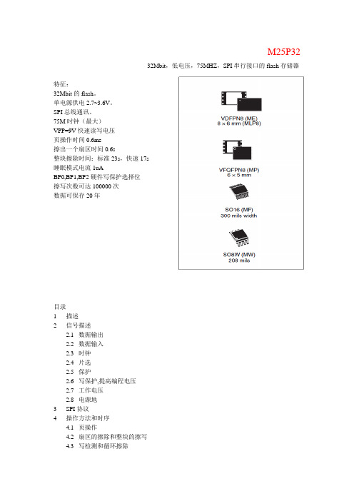
M25P3232Mbit,低电压,75MHZ,SPI串行接口的flash存储器特征:32Mbit的flash。
单电源供电2.7~3.6V。
SPI总线通讯。
75M时钟(最大)VPP=9V快速读写电压页操作时间0.6ms擦出一个扇区时间0.6s整块擦除时间:标准23s,快速17s睡眠模式电流1uABP0,BP1,BP2硬件写保护选择位擦写次数可达100000次数据可保存20年目录1描述2信号描述数据输出数据输入时钟片选保护写保护,提高编程电压工作电压电源地3SPI协议4操作方法和时序页操作扇区的擦除和整块的擦写写检测和循环擦除快速编程和擦除操作激活,正常工作,睡眠模式状态寄存器保护方法保持条件5存储组织结构6操作说明写操作使能使能复位读器件ID读状态寄存器WIP位WEL位BP2,BP1,BP0位SRWD位写状态寄存器读数据操作快速读数据操作页操作扇区擦除操作整个器件擦除睡眠模式激活器件78原始状态9极限参数10DC和AC参数11硬件结构12编号13修订记录1 描述M25P32是32Mbit(4M*8)的串行flash存储器,具有增强写保护结构。
存取采用SPI 总线协议。
一次性可编程1-256个字节(参考页编程操作说明)。
增强型快速编程、擦除模式可适用于需要快速存储的场合。
当V PPH 达到写保护或增强编程电压时即可进入此模式。
存储结构分为64个扇区,每个含有256页,每页256字节的宽度,所以整个器件可以看成有16384页组成(或者4194304个字节组成)整个器件的擦除(参考整块擦除说明),一次擦除一个扇区(参考扇区擦除说明)图1表1图22信号描述串行数据输出(Q)串行数据输入(D)图31.DU = Don’t use2.3 串行时钟信号2.4片选()当片选端输入为高时,那么取消选定器件,此时串行数据输出为高阻态,除非内部编程,循环对擦除、写寄存器进行操作,器件将工作在标准电源模式下(非睡眠模式)当器件片选信号拉低使能时,即器件进入正常工作模式。
- 1、下载文档前请自行甄别文档内容的完整性,平台不提供额外的编辑、内容补充、找答案等附加服务。
- 2、"仅部分预览"的文档,不可在线预览部分如存在完整性等问题,可反馈申请退款(可完整预览的文档不适用该条件!)。
- 3、如文档侵犯您的权益,请联系客服反馈,我们会尽快为您处理(人工客服工作时间:9:00-18:30)。
DESCRIPTIONThe 3823 group is the 8-bit microcomputer based on the 740 fam-ily core technology.The 3823 group has the LCD drive control circuit, an 8-channel A/ D converter, a serial interface, a watchdog timer, a ROM correc-tion function, and as additional functions.The various microcomputers in the 3823 group include variations of internal memory size and packaging. For details, refer to the section on part numbering.FEATURES●Basic machine-language instructions (71)●The minimum instruction execution time...........................0.4 µs (at f(X IN) = 10 MHz, High-speed mode)●Memory size ROM...............................................................16 K to 60 K bytes RAM.................................................................640 to 2560 bytes ●ROM correction function..............................32 bytes ✕ 2 blocks ●Watchdog timer..............................................................8-bit ✕ 1●Programmable input/output ports.. (49)●Input ports (5)●Software pull-up/pull-down resistors (Ports P0-P7 except port P40)●Interrupts.................................................17 sources, 16 vectors(includes key input interrupt)●Key Input Interrupt (Key-on Wake-Up) (8)●Timers...........................................................8-bit ✕ 3, 16-bit ✕ 2●Serial interface............8-bit ✕ 1 (UART or Clock-synchronized)●A/D converter............10-bit ✕ 8 channels or 8-bit ✕ 8 channels ●LCD drive control circuit Bias...................................................................................1/2, 1/3 Duty...........................................................................1/2, 1/3, 1/4 Common output.. (4)Segment output (32)●Main clock generating circuits..............Built-in feedback resistor(connect to external ceramic resonator or quartz-crystal oscillator)●Sub-clock generating circuits(connect to external quartz-crystal oscillator or on-chip oscillator)●Power source voltageIn frequency/2 mode (f(X IN) ≤ 10 MHz)...................4.5 to 5.5 V In frequency/2 mode (f(X IN) ≤ 8 MHz).....................4.0 to 5.5 V In frequency/4 mode (f(X IN) ≤ 10 MHz)...................2.5 to 5.5 V In frequency/4 mode (f(X IN) ≤ 8 MHz).....................2.0 to 5.5 V In frequency/4 mode (f(X IN) ≤ 5 MHz).....................1.8 to 5.5 V In frequency/8 mode (f(X IN) ≤ 10 MHz)...................2.5 to 5.5 V In frequency/8 mode (f(X IN) ≤ 8 MHz).....................2.0 to 5.5 V In frequency/8 mode (f(X IN) ≤ 5 MHz).....................1.8 to 5.5 V In low-speed mode....................................................1.8 to 5.5 V ●Power dissipationIn frequency/2 mode...............................................18 mW (std.) (at f(X IN) = 8 MHz, Vcc = 5 V, Ta = 25 °C)In low-speed mode at X CIN................................................18 µW (std.) (at f(X IN) stopped, f(X CIN) = 32 kHz, Vcc = 2.5 V, Ta = 25 °C)In low-speed mode at on-chip oscillator..................35 µW (std.) (at f(X IN) stopped, f(X CIN) = stopped, Vcc = 2.5 V, Ta = 25 °C)●Operating temperature range..................................– 20 to 85 °C APPLICATIONSCamera, audio equipment, household appliances, consumer elec-tronics, etc.3823 GroupSINGLE-CHIP 8-BIT CMOS MICROCOMPUTER REJ03B0146-0202Rev.2.02Jun.19.2007Table 1 Performance overviewParameter710.4 µs (Minimum instruction, f(X IN ) 10 MHz, High-speed mode)10 MHz (Maximum)16 K to 60 K bytes 640 to 2560 bytes 4-bit ✕ 1, 1-bit ✕ 1(4 pins sharing SEG)8-bit ✕ 5, 7-bit ✕ 1, 2 bit ✕ 1(16 pins sharing SEG)17 sources, 16 vectors (includes key input interrupt)8-bit ✕ 3, 16-bit ✕ 28-bit ✕ 1 (UART or Clock-synchronized)10-bit ✕ 8 channels or 8 bit ✕ 8 channels 8-bit ✕ 132 bytes ✕ 2 blocks 1/2, 1/32, 3, 4432Built-in feedback resistor(connect to external ceramic rasonator or quartz-crystal oscillator)Built-in feedback resistor(connect to external quartz-crystal oscillator or on-chip oscillator)4.5 to 5.5V 4.0 to 5.5V 2.5 to 5.5V 2.0 to 5.5V 1.8 to 5.5V 2.5 to 5.5V 2.0 to 5.5V 1.8 to 5.5V 1.8 to 5.5VStd. 18 mW (Vcc = 5V, f(X IN ) = 8MHz, Ta = 25 °C)Std. 18 µW (Vcc = 2.5V, f(X IN ) = stopped, f(X CIN ) = 32kHz, Ta = 25 °C)Std. 35 µW (Vcc = 2.5V, f(X IN ) = stopped, f(X CIN ) = stopped, Ta = 25 °C)V CC 10mA -20 to 85 °C CMOS sillicon gate80-pin plastic molded LQFP/QFPNumber of basic instructions Instruction execution time Oscillation frequency Memory sizes ROM RAM Input port P34-P37, P40I/O port P0-P2, P41-P47, P5, P6, P70, P71Interrupt TimerSerial interface A/D converter Watchdog timer ROM correction function LCD drive control Bias circuitDutyCommon output Segment outputMain clock generating circuits Sub-clock generating circuits Power source voltageIn frequency/2 mode (f(X IN ) ≤ 10MHz)In frequency/2 mode (f(X IN ) ≤ 8MHz)In frequency/4 mode (f(X IN ) ≤ 10MHz)In frequency/4 mode (f(X IN ) ≤ 8MHz)In frequency/4 mode (f(X IN ) ≤ 5MHz)In frequency/8 mode (f(X IN ) ≤ 10MHz)In frequency/8 mode (f(X IN ) ≤ 8MHz)In frequency/8 mode (f(X IN ) ≤ 5MHz)In low-speed modePower dissipationIn frequency/2 mode In low-speed mode at X CINIn low-speed mode at on-chip oscillatorInput/Output Input/Output withstand voltage characteristicsOutput current Operating temperature range Device structure PackageFunctionPIN DESCRIPTIONTable 2 Pin description (1)V CC , V SS FunctionPin Name Function except a port function•LCD segment output pinsPower source •Apply voltage of power source to V CC , and 0 V to V SS . (For the limits of V CC , refer to “Recom-mended operating conditions”).V REF AV SS RESET X IN X OUTV L1–V L3COM 0–COM 3SEG 0–SEG 11P00/SEG 16–P07/SEG 23P10/SEG 24–P17/SEG 31P20/KW 0 –P27/KW 7P34/SEG 12 –P37/SEG 15Analog refer-ence voltage Analog power source Reset input Clock input Clock outputLCD power sourceCommon outputSegment output I/O port P0I/O port P1I/O port P2•Reference voltage input pin for A/D converter.•GND input pin for A/D converter.•Connect to V SS .•Reset input pin for active “L”.•Input and output pins for the main clock generating circuit.•Feedback resistor is built in between X IN pin and X OUT pin.•Connect a ceramic resonator or a quartz-crystal oscillator between the X IN and X OUT pins to set the oscillation frequency.•If an external clock is used, connect the clock source to the X IN pin and leave the X OUT pin open.•This clock is used as the oscillating source of system clock.•Input 0 ≤ V L1 ≤ V L2 ≤ V L3 voltage.•Input 0 – V L3 voltage to LCD.•LCD common output pins.•COM 2 and COM 3 are not used at 1/2 duty ratio.•COM 3 is not used at 1/3 duty ratio.•LCD segment output pins.•8-bit I/O port.•CMOS compatible input level.•CMOS 3-state output structure.•I/O direction register allows each port to be individually programmed as either input or output.•Pull-down control is enabled.•8-bit I/O port.•CMOS compatible input level.•CMOS 3-state output structure.•I/O direction register allows each pin to be individually programmed as either input or output.•Pull-up control is enabled.•4-bit input port.•CMOS compatible input level.•Pull-down control is enabled.•Key input (key-on wake-up) interrupt input pins•LCD segment output pinsInput port P3Table 3 Pin description (2)FunctionPin Function except a port function P40P42/INT 0,P43/INT 1P44/R X D,P45/T X D,P46/S CLK ,P47/S RDY /S OUTP50/INT 2,P51/INT 3P52/RTP 0,P53/RTP 1P54/CNTR 0,P55/CNTR 1P56/T OUT P57/ADT P60/AN 0–P67/AN 7P70/X COUT,P71/X CIN•1-bit Input port.•CMOS compatible input level.•7-bit I/O port.•CMOS compatible input level.•CMOS 3-state output structure.•I/O direction register allows each pin to be individually programmed as either input or output.•Pull-up control is enabled.•8-bit I/O port.•CMOS compatible input level.•CMOS 3-state output structure.•I/O direction register allows each pin to be individually programmed as either input or output.•Pull-up control is enabled.•8-bit I/O port.•CMOS compatible input level.•CMOS 3-state output structure.•I/O direction register allows each pin to be individually programmed as either input or output.•Pull-up control is enabled.•2-bit I/O port.•CMOS compatible input level.•CMOS 3-state output structure.•I/O direction register allows each pin to be individually programmed as either input or output.•Pull-up control is enabled.•φ clock output pin •Interrupt input pins•Interrupt input pins •Real time port function pins •Timer X, Y function pins •Timer 2 output pins •A/D conversion input pins •Sub-clock generating circuit I/O pins.(Connect a resonator. External clock cannot be used.)P41/φ•Serial interface function pins•A/D trigger input pinsName I/O port P4I/O port P5I/O port P6I/O port P7Input port P4•QzROM program power pinPART NUMBERINGFig. 4 Part numbering Package codeFP :PRQP0080GB-A packageHP :PLQP0080KB-A packageROM numberOmitted in the shipped in blank version.ROM/PROM size1 :4096 bytes2 :8192 bytes3 :12288 bytes4 :16384 bytes5 :20480 bytes6 :24576 bytes7 :28672 bytes8 :32768 bytesThe first 128 bites and the last 2 bytes of ROM are reserved areas ; they cannot be used.Memory typeG :QzROM versionRAM size0 :192 bytes1 :256 bytes2 :384 bytes3 :512 bytes4 :640 bytes5 :768 bytes6 :896 bytes7 :1024 bytes8 :1536 bytes9 :2048 bytesA :2560 bytesProduct M38234G6-XXX FP9 :36864 bytesA :40960 bytesB :45056 bytesC :49152 bytesD :53248 bytesE :57344 bytesF :61440 bytesCurrently products are listed below.RemarksPackage Part No.RAM size (bytes)61440(61310)49152(49022)32768(32638)24576(24446)16384(16254)ROM size (bytes) ROM size for User in ( )Table 4 List of productsM3823AGF-XXXFP M3823AGF-XXXHP M3823AGFFP M3823AGFHPM38239GC-XXXFP M38239GC-XXXHP M38239GCFP M38239GCHPM38238G8-XXXFP M38238G8-XXXHP M38238G8FP M38238G8HPM38235G6-XXXFP M38235G6-XXXHP M38235G6FP M38235G6HPM38234G4-XXXFP M38234G4-XXXHP M38234G4FP M38234G4HP2560(Note 1)2048(Note 2)1536(Note 2)768(Note 2)640(Note 2)PRQP0080GB-A PLQP0080KB-A PRQP0080GB-A PLQP0080KB-A PRQP0080GB-A PLQP0080KB-A PRQP0080GB-A PLQP0080KB-A PRQP0080GB-A PLQP0080KB-A PRQP0080GB-A PLQP0080KB-A PRQP0080GB-A PLQP0080KB-A PRQP0080GB-A PLQP0080KB-A PRQP0080GB-A PLQP0080KB-A PRQP0080GB-A PLQP0080KB-ABlank BlankBlank BlankBlank BlankBlank BlankBlank BlankNote 1: RAM size includes RAM for LCD display and ROM corrections.Note 2: RAM size includes RAM for LCD display.FUNCTIONAL DESCRIPTIONCENTRAL PROCESSING UNIT (CPU)The 3823 group uses the standard 740 family instruction set. Re-fer to the table of 740 family addressing modes and machine instructions or the 740 Family Software Manual for details on the instruction set.Machine-resident 740 family instructions are as follows:The FST and SLW instruction cannot be used.The STP , WIT, MUL, and DIV instruction can be used.The central processing unit (CPU) has six registers. Figure 6shows the 740 Family CPU register structure.[Accumulator (A)]The accumulator is an 8-bit register. Data operations such as data transfer, etc., are executed mainly through the accumulator.[Index Register X (X)]The index register X is an 8-bit register. In the index addressing modes, the value of the OPERAND is added to the contents of register X and specifies the real address.[Index Register Y (Y)]The index register Y is an 8-bit register. In partial instruction, the value of the OPERAND is added to the contents of register Y and specifies the real address.[Stack Pointer (S)]The stack pointer is an 8-bit register used during subroutine calls and interrupts. This register indicates start address of stored area (stack) for storing registers during subroutine calls and interrupts.The low-order 8 bits of the stack address are determined by the contents of the stack pointer. The high-order 8 bits of the stack ad-dress are determined by the stack page selection bit. If the stack page selection bit is “0” , the high-order 8 bits becomes “0016”. If the stack page selection bit is “1”, the high-order 8 bits becomes “0116”.The operations of pushing register contents onto the stack and popping them from the stack are shown in Figure 7.Store registers other than those described in Table 4 with program when the user needs them during interrupts or subroutine calls.[Program Counter (PC)]The program counter is a 16-bit counter consisting of two 8-bit registers PC H and PC L . It is used to indicate the address of the next instruction to be executed.Fig. 6 740 Family CPU register structureAAccumulator b7b7b7b7b0b7b15b0b7b0b0b0b0XIndex register X YIndex register Y SStack pointer PC LProgram counter PC HN V T B D I Z CProcessor status register (PS)Carry flag Zero flagInterrupt disable flag Decimal mode flag Break flagIndex X mode flag Overflow flag Negative flag[Processor status register (PS)]The processor status register is an 8-bit register consisting of 5 flags which indicate the status of the processor after an arithmetic operation and 3 flags which decide MCU operation. Branch opera-tions can be performed by testing the Carry (C) flag , Zero (Z) flag, Overflow (V) flag, or the Negative (N) flag. In decimal mode, the Z, V, N flags are not valid.•Bit 0: Carry flag (C)The C flag contains a carry or borrow generated by the arithmetic logic unit (ALU) immediately after an arithmetic operation. It can also be changed by a shift or rotate instruction.•Bit 1: Zero flag (Z)The Z flag is set if the result of an immediate arithmetic operation or a data transfer is “0”, and cleared if the result is anything other than “0”.•Bit 2: Interrupt disable flag (I)The I flag disables all interrupts except for the interrupt generated by the BRK instruction.Interrupts are disabled when the I flag is “1”.•Bit 3: Decimal mode flag (D)The D flag determines whether additions and subtractions are executed in binary or decimal. Binary arithmetic is executed when this flag is “0”; decimal arithmetic is executed when it is “1”.Decimal correction is automatic in decimal mode. Only the ADC and SBC instructions can be used for decimal arithmetic.•Bit 4: Break flag (B)The B flag is used to indicate that the current interrupt was generated by the BRK instruction. The BRK flag in the processor status register is always “0”. When the BRK instruction is used to generate an interrupt, the processor status register is pushed onto the stack with the break flag set to “1”.•Bit 5: Index X mode flag (T)When the T flag is “0”, arithmetic operations are performed between accumulator and memory. When the T flag is “1”, direct arithmetic operations and direct data transfers are enabled between memory locations.•Bit 6: Overflow flag (V)The V flag is used during the addition or subtraction of one byte of signed data. It is set if the result exceeds +127 to -128. When the BIT instruction is executed, bit 6 of the memory location operated on by the BIT instruction is stored in the overflow flag.•Bit 7: Negative flag (N)The N flag is set if the result of an arithmetic operation or data transfer is negative. When the BIT instruction is executed, bit 7 of the memory location operated on by the BIT instruction is stored in the negative flag.Table 6 Set and clear instructions of each bit of processor status registerSet instruction Clear instruction C flagSECCLCZ flag––I flagSEICLID flagSEDCLDB flag––T flagSETCLTV flag–CLVN flag––Real time port function output A/D conversion inputA/D trigger inputDiagram No.Related SFRs Input/Output Name Pin Non-Port Function I/O Format Table 7 List of I/O port functionP00/SEG 16–P07/SEG 23P10/SEG 24–P17/SEG 31P20/KW 0–P27/KW 7P34/SEG 12–P37/SEG 15P40P41/φP42/INT 0,P43/INT 1P44/R X D P45/T X D P46/S CLK P47/S RDY /S OUTP50/INT 2,P51/INT 3P52/RTP 0,P53/RTP 1P54/CNTR 0Port P0Port P1Port P2Port P3Port P4Input/output,individual portsInput/output,individual bits InputInputInput/output,individual bitsCMOS compatible input levelCMOS 3-state outputCMOS compatible input levelCMOS 3-state output CMOS compatible input level CMOS compatible input levelCMOS compatible input levelCMOS 3-state outputCMOS compatible input levelCMOS 3-state outputCMOS compatible input levelCMOS 3-state output CMOS compatible input levelCMOS 3-state output LCD segment outputKey input (key-on wake-up) interrupt inputLCD segment outputφ clock outputX CIN frequency signal outputExternal interrupt inputSerial I/O function input/outputExternal interrupt input Timer X function I/O Timer Y function input Timer 2 function output PULL register A Segment output enable registerPULL register AInterrupt control register 2PULL register ASegment output enable registerPULL register Bφ output control register Peripheral function extension register PULL register BInterrupt edge selection registerPULL register BSerial I/O control register Serial I/O status register UART control register Peripheral function extension register PULL register BInterrupt edge selection registerPULL register BTimer X mode register PULL register BTimer X mode register PULL register BTimer Y mode register PULL register BTimer 123 mode register PULL register B A/D control registerPULL register A CPU mode register (1)(2)(3)(4)(6)(5)(2)(8)(7)Port P5(9)(2)Input/output,individual bits(10)P55/CNTR 1(11)(12)(13)(12)(14)P56/T OUT P57/ADT P60/AN 0–P67/AN 7(15)P70/X COUT P71/X CIN COM 0–COM 3SEG 0–SEG 11(16)(17)(18)Input/output,individual bits Input/output,individual bits Output OutputSub-clockgenerating circuit I/O LCD common output LCD segment outputPort P6Port P7Common SegmentLCD mode registerNotes 1: For details of how to use double function ports as function I/O ports, refer to the applicable sections.2: When an input level is at an intermediate potential, a current will flow from V CC to V SS through the input-stage gate.Especially, power source current may increase during execution of the STP and WIT instructions.Fix the unused input pins to “H” or “L” through a resistor.QzROM program power pinTermination of unused pins• Termination of common pinsI/O ports:Select an input port or an output port and follow each processing method.Output ports: Open.Input ports:If the input level become unstable, through current flow to an input circuit, and the power supply currentmay increase.Especially, when expecting low consumption current(at STP or WIT instruction execution etc.), pull-up orpull-down input ports to prevent through current(built-in resistor can be used). Pull-down the P40/(V PP) pin.We recommend processing unused pins through aresistor which can secure I OH(avg) or I OL(avg).Because, when an I/O port or a pin which have anoutput function is selected as an input port, it mayoperate as an output port by incorrect operation etc.Table 8 Termination of unused pinsPinP00/SEG16–P17/SEG23 P10/SEG24–P17/SEG31 P20/KW0–P27/KW7P34/SEG12–P37/SEG15 P40/(V PP)P41/φP42/INT0P43/INT1P44/RxDP45/TxDP46/S CLKP47/S RDY/S OUTP50/INT2P51/INT3P52/RTP0P53/RTP1P54/CNTR0P55/CNTR1P56/T OUTP57/ADTP60/AN0–P67/AN7P70/X COUTP71/X CINV L3 (Note)V L2 (Note)V L1 (Note)COM0–COM3SEG0–SEG11AV SSV REFX OUTTermination 2When selecting SEG output, open.When selecting KW function, performtermination of input port.When selecting SEG output, open.–When selecting φ output, open.When selecting INT0 function,perform termination of input port.When selecting INT1 function,perform termination of input port.When selecting R X D function,perform termination of input port.When selecting T X D function,perform termination of output port.When selecting external clock input,perform termination of input port.When selecting S RDY function,perform termination of output port.When selecting INT2 function,perform termination of input port.When selecting INT3 function,perform termination of input port.When selecting RTP0 function,perform termination of output port.When selecting RTP1 function,perform termination of output port.When selecting CNTR0 input function,perform termination of input port.When selecting CNTR1 function,perform termination of input port.When selecting T OUT function,perform termination of output port.When selecting ADT function,perform termination of input port.When selecting AN function, thesepins can be opened. (A/D conversionresult cannot be guaranteed.)Do not select X CIN-X COUT oscillationfunction by program.––––––––Termination 3–––––––––When selecting internal clock output,perform termination of output port.When selecting S OUT function,perform termination of output port.––––When selecting CNTR0 output function,perform termination of output port.–––––––––––––Termination 1 (recommend)I/O portInput portInput port (pull-down)I/O portConnect to V SSConnect to V SSConnect to V SSOpenOpenConnect to V SSConnect to V CC or V SSWhen an external clock isinput to the X IN pin, leavethe X OUT pin open.Note :The termination of V L3, V L2 and V L1 is applied when the bit 3 of the LCD mode register is “0”INTERRUPTSThe 3823 group interrupts are vector interrupts with a fixed prior-ity scheme, and generated by 16 sources among 17 sources: 8external, 8 internal, and 1 software.The interrupt sources, vector addresses (1) , and interrupt priority are shown in Table 9.Each interrupt except the BRK instruction interrupt has the inter-rupt request bit and the interrupt enable bit. These bits and the interrupt disable flag (I flag) control the acceptance of interrupt re-quests. Figure 16 shows an interrupt control diagram.Notes1: Vector addresses contain interrupt jump destination addresses.2: Reset function in the same way as an interrupt with the highest priority.Table 9 Interrupt vector addresses and priorityRemarksInterrupt Request Generating Conditions At resetAt detection of either rising or falling edge of INT 0 input At detection of either rising or falling edge of INT 1 input At completion of serial interface data receptionAt completion of serial interface transmit shift or when transmis-sion buffer is empty Interrupt Source LowHigh PriorityVector Addresses (Note 1)Reset (Note 2)INT 0INT 1Serial I/O reception Serial I/O transmission Timer X Timer Y Timer 2Timer 3CNTR 0CNTR 1Timer 1INT 2INT 3Key input(Key-on wake-up)ADTA/D conversion BRK instruction1234567891011121314151617FFFD 16FFFB 16FFF916FFF716FFF516FFF316FFF116FFEF 16FFED 16FFEB 16FFE916FFE716FFE516FFE316FFE116FFDF 16FFDD 16FFFC 16FFFA 16FFF816FFF616FFF416FFF216FFF016FFEE 16FFEC 16FFEA 16FFE816FFE616FFE416FFE216FFE016FFDE 16FFDC 16At timer X underflow At timer Y underflow At timer 2 underflowAt timer 3 underflowAt detection of either rising or falling edge of CNTR 0 input At detection of either rising or falling edge of CNTR 1 input At timer 1 underflowAt detection of either rising or falling edge of INT 2 input At detection of either rising or falling edge of INT 3 input At falling of conjunction of input level for port P2 (at input mode)At falling of ADT inputAt completion of A/D conversion At BRK instruction executionNon-maskableExternal interrupt(active edge selectable)External interrupt(active edge selectable)Valid when serial interface is se-lectedValid when serial interface is se-lectedExternal interrupt(active edge selectable)External interrupt(active edge selectable)External interrupt(active edge selectable)External interrupt(active edge selectable)External interrupt (Valid at falling)Valid when ADT interrupt is se-lected, External interrupt (Valid at falling)Valid when A/D interrupt is se-lectedNon-maskable software interruptAn interrupt requests is accepted when all of the following conditions are satisfied:• Interrupt disable flag.................................“0”• Interrupt disable request bit .....................“1”• Interrupt enable bit.. (1)Though the interrupt priority is determined by hardware, priority processing can be performed by software using the above bits and flag.[Transmit Buffer/Receive Buffer Register (TB/RB)] 001816The transmit buffer register and the receive buffer register are lo-cated at the same address. The transmit buffer register is write-only and the receive buffer register is read-only. If a charac-ter bit length is 7 bits, the MSB of data stored in the receive buffer register is “0”.[Serial I/O Status Register (SIOSTS)] 001916 The read-only serial I/O status register consists of seven flags (bits 0 to 6) which indicate the operating status of the serial I/O function and various errors.Three of the flags (bits 4 to 6) are valid only in UART mode.The receive buffer full flag (bit 1) is cleared to “0” when the receive buffer is read.If there is an error, it is detected at the same time that data is transferred from the receive shift register to the receive buffer reg-ister, and the receive buffer full flag is set. A write to the serial I/O status register clears all the error flags OE, PE, FE, and SE. Writ-ing “0” to the serial I/O enable bit (SIOE) also clears all the status flags, including the error flags.All bits of the serial I/O status register are initialized to “0” at reset, but if the transmit enable bit (bit 4) of the serial I/O control register has been set to “1”, the transmit shift register shift completion flag (bit 2) and the transmit buffer empty flag (bit 0) become “1”. [Serial I/O Control Register (SIOCON)] 001A16 The serial I/O control register contains eight control bits for the se-rial I/O function.[UART Control Register (UARTCON) ]001B16 The UART control register consists of four control bits (bits 0 to 3) which are valid when asynchronous serial I/O is selected and set the data format of an data transfer. One bit in this register (bit 4) is always valid and sets the output structure of the P45/T X D pin. [Baud Rate Generator (BRG)] 001C16The baud rate generator determines the baud rate for serial trans-fer.The baud rate generator divides the frequency of the count source by 1/(n + 1), where n is the value written to the baud rate genera-tor.■Notes on serial I/OWhen setting the transmit enable bit to “1”, the serial I/O transmit interrupt request bit is automatically set to “1”. When not requiring the interrupt occurrence synchronized with the transmission enalbed, take the following sequence.➀Set the serial I/O transmit interrupt enable bit to “0” (disabled).➁Set the transmit enable bit to “1”.➂Set the serial I/O transmit interrupt request bit to “0” after 1 or more instructions have been executed.➃Set the serial I/O transmit interrupt enable bit to “1” (enabled).。