ATA016A0X3Z;ATA016A0X3;ATA016A0X43Z;中文规格书,Datasheet资料
希捷硬盘固件指令要领
B级自修复指令:T>后输入N3,,22, 回车载入,再按CTRL+T启动B级自修复。
A级自校准指令:T>后输入N2,,22, 回车载入,再按CTRL+T启动A级自校准。
B级自校准指令:T>后输入N2,AA,22, 回车载入,再按CTRL+T启动B级自校准。
工厂坏道修复指令:T>后输入N30,,22, 回车载入,再按CTRL+T启动工厂坏道修复。
停止自校准指令:T>后输入N50,,22, 按回车执行,停止硬盘自校准。
内部轨
关闭酷鱼4、5、6代磁头指令:T>后输入YA0, 回车载入,关闭损坏磁头。
希捷硬盘固件指令要领
希捷硬盘固件:
希捷盘的固件也是在硬盘的负道区,用十六进制数标记固件的具体位置,通过COM线访问这个区域。在维修时主要用到三个位置的固件,通常叫做ATA模块,CERT模块及VEN模块。
希捷硬盘指令维修:
连好COM线和电源线后(不需要接IDE线)接上后程序出现返回信息,MASTER........,表示硬盘已经认盘。出现MASTER....后,按键盘CTRL+Z,让硬盘进入待命模式,出现T>后,在按键盘的“;”键,COM口就返回硬盘的一些重要信息:AGE=50表示硬盘AGE值是正常的,如果是其他值硬盘就有故障,TYPE=20表示硬盘磁头型号是2型磁头,MxHd=0表示硬盘只有一个磁头,两个磁头就是=1,依次类推。
拿到一个有坏道或者不认盘的希捷盘,都要先接上COM线,看看返回信息是不是正常,返回信息正常后才可以对硬盘进行修复。少量坏道建议用自修复,大量坏道,不稳定坏道需用自校准修复。
电脑错误代码大全[a]
![电脑错误代码大全[a]](https://img.taocdn.com/s3/m/6dc345adb8d528ea81c758f5f61fb7360b4c2be3.png)
电脑错误代码大全[a]0000 操作已成功完成。
0001 错误的函数。
0002 系统找不到指定的文件。
0003 系统找不到指定的路径。
0004 系统无法打开文件。
0005 拒绝访问。
0006 句柄无效。
0007 存储区控制块已损坏。
0008 可用的存储区不足,无法执行该命令。
0009 存储区控制块地址无效。
0010 环境错误。
0011 试图使用不正确的格式加载程序。
0012 访问代码无效。
0013 数据无效。
0014 可用的存储区不足,无法完成该操作。
0015 系统找不到指定的驱动器。
0016 无法删除该目录。
0017 系统无法将文件移到其他磁盘驱动器上。
0018 没有其他文件。
0019 媒体写保护。
0020 系统找不到指定的设备。
0021 设备尚未准备好。
0022 设备无法识别该命令。
0023 数据错误(循环冗余检查)。
0024 程序发出命令,但是该命令的长度错误。
0025 驱动器在磁盘上无法定位指定的区域或磁道。
0026 无法访问指定的磁盘或软盘。
0027 驱动器找不到所请求的扇区。
0028 打印机缺纸。
0029 系统无法写入指定的设备。
0030 系统无法读取指定的设备。
0031 与系统连接的设备不能正常运转。
0032 其他进程正使用该文件,因此现在无法访问。
0033 另一进程已锁定该文件的某一部分,因此现在无法访问。
0034 驱动器中的软盘不正确。
请将 %2 (卷标序列号: %3)插入驱动器 %1。
0036 打开共享的文件太多。
0038 已到达文件结尾。
0039 磁盘已满。
0050 不支持此网络请求。
0051 远程计算机无法使用。
0052 网络中存在重名。
0053 找不到网络路径。
0054 网络正忙。
0055 指定的网络资源或设备已不可用。
0056 已经达到网络命令的极限。
0057 网络适配器出现错误。
0058 指定的服务器无法执行所请求的操作。
0059 网络出现意外错误。
0060 远程适配器不兼容。
计算机故障中英文对照表
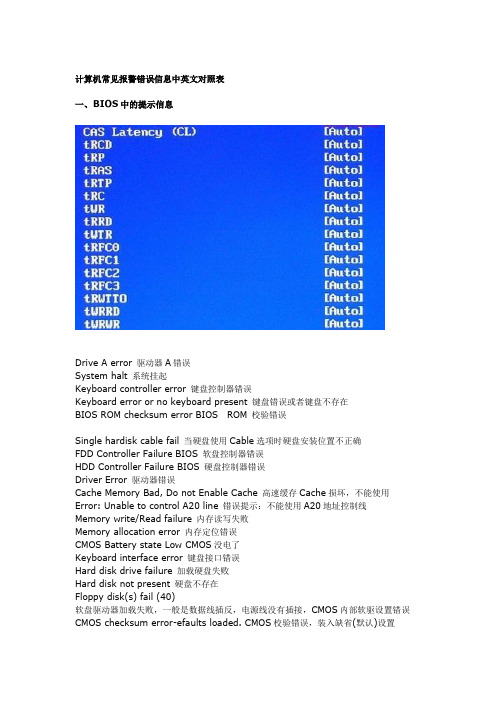
计算机常见报警错误信息中英文对照表一、B IOS中的提示信息Drive A error 驱动器A错误System halt 系统挂起Keyboard controller error 键盘控制器错误Keyboard error or no keyboard present 键盘错误或者键盘不存在BIOS ROM checksum error BIOS ROM 校验错误Single hardisk cable fail 当硬盘使用Cable选项时硬盘安装位置不正确FDD Controller Failure BIOS 软盘控制器错误HDD Controller Failure BIOS 硬盘控制器错误Driver Error 驱动器错误Cache Memory Bad, Do not Enable Cache 高速缓存Cache损坏,不能使用Error: Unable to control A20 line 错误提示:不能使用A20地址控制线Memory write/Read failure 内存读写失败Memory allocation error 内存定位错误CMOS Battery state Low CMOS没电了Keyboard interface error 键盘接口错误Hard disk drive failure 加载硬盘失败Hard disk not present 硬盘不存在Floppy disk(s) fail (40)软盘驱动器加载失败,一般是数据线插反,电源线没有插接,CMOS内部软驱设置错误CMOS checksum error-efaults loaded. CMOS校验错误,装入缺省(默认)设置二、BIOS刷新失败后,Bootblock启动时出现的提示信息Detecting floppy drive A media... 检测软驱A的格式Drive media is : 1.44Mb1.2Mb 720Kb 360K驱动器格式是1.44Mb、12Mb、720kb、360kb的一种DISK BOOT FAILURE, INSERT SYSTEM DISK AND PRESS ENTER磁盘引导失败,插入系统盘后按任意键继续三、MBR主引导区提示信息Invalid partition table 无效的分区表Error loading operating sy stem 不能装入引导系统Missing operating system 系统引导文件丢失说明:如果在计算机启动过程中,在硬件配置清单下方(也就时在平时正常启动时出现Starting Windows 98…的地方)出现不可识别字符,此时可判断硬盘分区表损坏。
48bits的ata命令

48bits的ata命令
ATA(Advanced Technology Attachment)是一种计算机接口标准,用于连接存储设备(如硬盘驱动器)到计算机系统。
48位的
ATA命令是指在ATA协议中使用48位寻址方式进行数据传输和操作
的命令。
48位的ATA命令相比于之前的28位ATA命令,提供了更大的
寻址范围,可以支持更大容量的硬盘驱动器。
28位ATA命令最大支
持的寻址范围是2^28个扇区,每个扇区大小为512字节,因此最大
支持的容量为137.4GB。
而48位ATA命令则可以支持的寻址范围是
2^48个扇区,最大支持的容量可以达到128PB(1PB=1024TB)。
使用48位ATA命令可以带来许多优势。
首先,它允许支持更大
容量的硬盘驱动器,使得用户可以存储更多的数据。
其次,通过增
加寻址范围,48位ATA命令可以提高数据传输的效率和速度。
此外,它还支持更高级的功能和特性,如数据加密、错误检测和修复等。
在实际应用中,使用48位ATA命令的硬盘驱动器需要操作系统
和主板的支持。
操作系统需要支持48位寻址方式,并且主板的
BIOS也需要更新以支持48位ATA命令。
如果系统不支持48位ATA
命令,那么即使使用了支持更大容量的硬盘驱动器,也只能使用28位ATA命令的寻址范围。
总结来说,48位的ATA命令是一种支持更大容量硬盘驱动器的命令,它提供了更大的寻址范围和更高级的功能,可以提高数据传输效率和速度。
然而,使用48位ATA命令需要操作系统和主板的支持。
thinkpad bios中英对照

VIsable)
Enable:启用快取功能以加快显示速度。
Disable:取消此功能。
MemoryHoleatAddress(默认值为None)
一些ISA卡会要求使用14-16MB或15-16MB的记忆地址空间,若选取14MB-16MB或 15MB-16MB,系统将无法使用这部份的内存空间。您可选取None来取消此功能。
当同时安装SCSI及IDE硬盘时,本选项功能可用来选择以SCSI或IDE硬盘作为启动盘。
BootSequence(开机顺序,默认值为C,A)
此选项设定当计算机开机时,选择由A盘,C盘及CD-ROM开机的优先级。
SwapFloppyDrive(软盘机互换,默认值为Disable)
NORMAL模式:为传统标准模式,支持硬盘机容量最高至528MB。
LBA(LogicalBlockAddressingMode)模式:适用于硬盘容量超过且支持逻辑区块LARGE模式:当硬盘机容量超过528MB,而硬盘或操作系统不支持LBA模式时,可采用此选项。
DriverA/DriverB(None)
[特别注意]:当您安装新的操作系统(如Win98)时,请先取消(disable)此功能,以免因衡突而无法顺利安装。
CPUInternalCache(CPU内部高速缓存,默认值为Enable)
本项功能用于启用(enable)或取消(disable)CPULevel1高速缓存。就整体速度而言,启用L1快取将比取消L1快取时提升许多。因此,默认值为启用(enable)。
AutoConfiguration(自动设定,默认值为60nsDRAM)
您可依照您所使用的内存来选取60MDRAMor70NSDRAM选项,BIOS会根据您的设定自动调整第2到9选项。若选择“disable”(取消),则第2至第9选项可自行调整。
THINKPAD开机错误消息及报警信息详解

THINKPAD开机错误消息及报警信息详解注:在图表中,x 可以是任何字符。
0175: Bad CRC1, stop POST task(CRC1 错误,停止POST 任务)0176: System Security - The system has been tampered with.(系统安全性- 系统受到了干扰。
)0177: Bad SVP data, stop POST task.(SVP 数据错误,停止POST 任务。
)0182: Bad CRC2.Enter BIOS Setup and load Setup defaults.(CRC2 错误。
请进入BIOS Setup 并装入Setup 缺省值。
)0185: Bad startup sequence settings. Enter BIOS Setup and load Setup defaults.(CRC2 错误。
请进入BIOS Setup 并装入Setup 缺省值。
)0187: EAIA data access error(EAIA 数据访问错误)0188: Invalid RFID Serialization Information Area.(无效的RFID 序列化信息区域。
)0189: Invalid RFID configuration information area(无效的RFID 配置信息区域)0190: Critical low-battery error(电池电量严重不足错误)0191: System Security - Invalid remote change requested.(系统安全性-请求了无效的远程更改。
)0192: System Security - Embedded Security hardware tamper detected.(系统安全性-检测到Embedded Security 硬件窜改。
ATA协议学习笔记

(3)UDMA(Ultra DMA),也是用于数据传输。
这种传输方式的传输速度比MDM A要快,ATA/ATAPI-5协议中所定义的UDMA传输方式最高数据传输速率是66MB/ s。
UDMA对数据传输的控制信号重新进行了定义。
另外,UDMA还引入了CRC数据校验机制,保证了数据传输过程的正确性,但其传输过程较为复杂。
4、ATA接口寄存器的定义ATA主机与设备的通信是通过主机对ATA接口上的寄存器的读写实现的,而这些接口寄存器由主机发送的地址信号CS1_、CS0_、DA2、DA1、DA0来进行寻址。
除了在DMA传输模式下,CS1_和CS0_全有效或全无效都是不可用的地址,在这种情况下,数据线应该在释放状态下(即数据总线没有驱动源)。
当CS0_无效,C S1_有效时,DA[2:0]只有在值为06H和07H时地址才为有效,在其他的无效地址状态下,设备会使数据总线处于高阻态。
ATA接口寄存器可分为命令块寄存器和控制块寄存器。
(1)命令块寄存器是主机用来向设备传输命令或从设备读取状态的,这组寄存器包括:柱面号高(Cylinder High)8位寄存器柱面号低(Cylinder Low)8位寄存器设备/磁头(Device/Head)寄存器扇区数(Sector Count)寄存器扇区号(Sector Number)寄存器命令(Command)寄存器状态(Status)寄存器特征(Features)寄存器错误(Error)寄存器数据(Data)寄存器。
(2)控制块寄存器是用来控制设备和替换状态,这组寄存器包括:设备控制(Device Control)寄存器替换状态(Alternate Status)寄存器驱动器地址(Drive Address)寄存器。
asus-as016

AS-016SpecificationBlock DiagramPin AssignmentRev.0.001October 16,2002PreliminaryFeatures·16-pin SOP packageGeneral DescriptionThis ASIC is designed to reduce the discrete logics used in the mother board.With this device,the mother board ¢s reliability is increased,while its size and cost are reduced.The function of this device is to regulate the power con-trol of the mother board.The RSMRST#signal is used to identify the status of the 5VSB.The 3VSBSW#signalis used to select the 3.3V power source.The PWRGD1and PWRGD2signals are used to indicate whether the power is OK or not.The PSONOUT#signal is used to control the On and Off of the power supply.The BRSTDRV#and PCIRST#signals are used to reset the devices.Pin DescriptionPin No.Pin Name I/O Spec.Description Power&reset control:8pins16RSMRST#@VDD=VBAT(3.3V)O/P spec:NMOS ODI OL=4mA/0.4VPull-high5V toleranceThis is the+5VSB power good signal,with Schmitt triggerinput,the high threshold is4V±0.2V,and the low threshold is3.5V±0.2V6RESETCON#@VDD=5VSBI/P spec:TTL inputInternal pull-high100k W to5VSBThis pin connects to the reset button,and also to the other re-set source on the motherboard.Low reset chip(5V logic)PWRGD follows with RESETCON12PWRGD1@VDD=5VSBO/P spec:NMOS ODI OL=10mA/0.4V5V>4volt,wait for425ms then rising PWRGD to high5V<3.5volt,then falling PWRGD to lowThis pin also follows with RESETCON13PWRGD2@VDD=5VSBO/P spec:NMOS ODI OL=10mA/0.4V5V>4volt,wait for425ms then rising PWRGD to high5V<3.5volt,then falling PWRGD to lowThis pin also follows with RESETCON7RSTIN#@VDD=VDD5VSBI/P spec:TTL inputInternal pull-high100k W to5VSBOriginal Reset signal from chipset9PCIRST#@VDD=VDD5VSBO/P spec:CMOS O/PI OL=16mA/0.4VI OH=16mA/4.5VReset for add-on PCI card10BRSTDRV#@VDD=VDD5VSBO/P spec:CMOS O/PI OL=16mA/0.4VI OH=16mA/4.5VReset for IDE11PSONOUT#@VDD=5VSBO/P spec:NMOS ODI OL=10mA/0.4VPSON#signal to power supplyPSONOUT#=NOT(SUSB#)Propagation delay=125m s~250m sSuspend control:4pin4SUSB#@VDD=5VSBI/P spec:TTL inputInternal pull-high100k W to5VSBSUSB#signal from Intel/VIA South Bridge.High at S0~S2andturn low when S3/S4/S55SUSC#@VDD=5VSBI/P spec:TTL inputInternal pull-high100k W to5VSBSUSC#signal from Intel/VIA South Bridge.High at S0~S3andturn low when S4/S5153VSBSW#@VDD=5VSBO/P spec:CMOS O/PI OL=4mA/0.4VI OH=4mA/4.5VActive low when system enters the S3state until system en-ters the S0state and PWRGD is active high3G3VSBSW#@VDD=5VSBI/P spec:TTL inputInternal pull-low100k W to GNDSignal used for gating off3VSBSW#Low:Gating off3VSBSW#(default,BIOS will program lowwhen power on)High:not gating off3VSBSW#(BIOS will program high beforeentering S3state)This signal will be transparent while PWRGD is high internallyand latched with the falling edge of SUSB#.Rev.0.002October16,2002Pin No.Pin Name I/O Spec.DescriptionPower/GND:4pin145V Power25VSB Power1VBAT Power3GND GNDAbsolute Maximum RatingsSupply Voltage........................................-0.3V to5.5V Storage Temperature...........................-50°C to125°C Input Voltage.............................V SS-0.3V to V DD+0.3V Operating Temperature..........................-25°C to70°CNote:These are stress ratings only.Stresses exceeding the range specified under²Absolute Maximum Ratings²may cause substantial damage to the device.Functional operation of this device at other conditions beyond those listed in the specification is not implied and prolonged exposure to extreme conditions may affect device reliabil-ity.D.C.Characteristics Ta=25°C,VDD5V=5V,VDD5VSB=5V,VBAT=3.3VPin Name Symbol I/O Spec.&Test Condition Min.Typ.Max.UnitVBAT I OP VDD5VSB=5V,VDD5V=5V¾¾5m A I SB VDD5VSB=0V,VDD5V=0V¾¾1m AVDD5VSB I OP VBAT=3.3V,VDD5V=5V¾¾5mA I SB VBAT=3.3V,VDD5V=0V¾¾1mAVDD5V I OP VBAT=3.3V,VDD5V=5V¾¾5mA RSMRST#I OL VBAT=3.3V,V OL=0.4V46¾mARESETCON# RSTIN# SUSB# SUSC#V IL VDD5VSB=5V0¾0.8V V IH VDD5VSB=5V2¾5V R H VDD5VSB=5V,V IL=0V60100150K WG3VSBSW#V IL VDD5VSB=5V0¾0.8V V IH VDD5VSB=5V2¾5V R L VDD5VSB=5V,V IH=5V85125165K W3VSBSW#I OL VDD5VSB=5V,V OL=0.4V4¾¾mA I OH VDD5VSB=5V,V OH=4.5V4¾¾mAPWRGD1PWRGD2PSONOUT#I OL VDD5VSB=5V,V OL=0.4V10¾¾mAPCIRST# BRSTDRV#I OL VDD5VSB=5V,V OL=0.4V16¾¾mA I OH VDD5VSB=5V,V OH=4.5V16¾¾mARev.0.003October16,2002A.C.Characteristics Ta=25°C,VDD5V=5V,VDD5VSB=5V,VBAT=3.3V Symbol Parameter Min.Typ.Max.UnitTd1Power Good Delay300425600msTd2RSMRST#Delay406090ms ·Power good delay·RSMRST#delayTiming DiagramsFrom S0to S3(SW off to on)From S3to S0(SW on to off)From S5to S0and from S0to S5(not SW on)Rev.0.004October16,2002Package Information16-pin NSOP(150mil)outline dimensionsSymbolDimensions in milMin.Nom.Max.A228¾244B149¾157C14¾20C¢386¾394D53¾69E¾50¾F4¾10G22¾28H4¾12a0°¾10°Rev.0.005October16,2002Product Tape and Reel SpecificationsReel dimensionsSOP16NSymbol Description Dimensions in mmA Reel Outer Diameter330±1.0B Reel Inner Diameter62±1.5C Spindle Hole Diameter12.75+0.5D Key Slit Width 1.5+0.15T1Space Between Flange16.4+0.2T2Reel Thickness22.4+0.4Rev.0.006October16,2002Carrier tape dimensionsSOP16NSymbol Description Dimensions in mm W Carrier Tape Width16.0±0.3P Cavity Pitch8.0±0.1E Perforation Position 1.75±0.1F Cavity to Perforation(Width Direction)7.5±0.1D Perforation Diameter 1.55+0.1D1Cavity Hole Diameter 1.5+0.25P0Perforation Pitch 4.0±0.1P1Cavity to Perforation(Length Direction) 2.0±0.1A0Cavity Length 6.5±0.1B0Cavity Width10.3±0.1K0Cavity Depth 2.1±0.1t Carrier Tape Thickness0.3±0.05C Cover Tape Width13.3Rev.0.007October16,2002Holtek Semiconductor Inc.(Headquarters)No.3,Creation Rd.II,Science-based Industrial Park,Hsinchu,TaiwanTel:886-3-563-1999Fax:886-3-563-1189Holtek Semiconductor Inc.(Sales Office)11F,No.576,Sec.7Chung Hsiao E.Rd.,Taipei,TaiwanTel:886-2-2782-9635Fax:886-2-2782-9636Fax:886-2-2782-7128(International sales hotline)Holtek Semiconductor(Shanghai)Inc.7th Floor,Building2,No.889,Yi Shan Rd.,Shanghai,ChinaTel:021-6485-5560Fax:021-6485-0313Holtek Semiconductor(Hong Kong)Ltd.RM.711,Tower2,Cheung Sha Wan Plaza,833Cheung Sha Wan Rd.,Kowloon,Hong KongTel:852-2-745-8288Fax:852-2-742-8657Holmate Semiconductor,Inc.48531Warm Springs Boulevard,Suite413,Fremont,CA94539Tel:510-252-9880Fax:510-252-9885CopyrightÓ2002by HOLTEK SEMICONDUCTOR INC.The information appearing in this Data Sheet is believed to be accurate at the time of publication.However,Holtek as-sumes no responsibility arising from the use of the specifications described.The applications mentioned herein are used solely for the purpose of illustration and Holtek makes no warranty or representation that such applications will be suitable without further modification,nor recommends the use of its products for application that may present a risk to human life due to malfunction or otherwise.Holtek reserves the right to alter its products without prior notification.For the most up-to-date information,please visit our web site at .Rev.0.008October16,2002。
- 1、下载文档前请自行甄别文档内容的完整性,平台不提供额外的编辑、内容补充、找答案等附加服务。
- 2、"仅部分预览"的文档,不可在线预览部分如存在完整性等问题,可反馈申请退款(可完整预览的文档不适用该条件!)。
- 3、如文档侵犯您的权益,请联系客服反馈,我们会尽快为您处理(人工客服工作时间:9:00-18:30)。
Data SheetOctober 1, 2009Austin SuperLynx TM II 12V SIP Non-isolated Power Modules:8.3Vdc – 14Vdc input; 0.75Vdc to 5.5Vdc Output; 16A Output Current* UL is a registered trademark of Underwriters Laboratories, Inc. †CSA is a registered trademark of Canadian Standards Association. ‡VDE is a trademark of Verband Deutscher Elektrotechniker e.V.ApplicationsDistributed power architectures Intermediate bus voltage applications Telecommunications equipment Servers and storage applications Networking equipment Enterprise NetworksLatest generation IC’s (DSP, FPGA, ASIC) and Microprocessor powered applicationsFeaturesCompliant to RoHS EU Directive 2002/95/EC (-Z versions)Compliant to ROHS EU Directive 2002/95/EC with lead solder exemption (non-Z versions) Flexible output voltage sequencing EZ-SEQUENCE TMDelivers up to 16A output currentHigh efficiency – 92% at 3.3V full load (V IN = 12.0V)Small size and low profile: 50.8 mm x 12.7 mm x 8.1 mm (2.00 in x 0.5 in x 0.32 in) Low output ripple and noiseConstant switching frequency (300KHz) High Reliability:Calculated MTBF = 9.2M hours at 25oC Full-load Programmable Output voltage Line Regulation: 0.3% (typical) Load Regulation: 0.4% (typical) Temperature Regulation: 0.4 % (typical)Remote On/Off Remote SenseOutput overcurrent protection (non-latching) Wide operating temperature range (-40°C to 85°C)UL * 60950-1Recognized, CSA †C22.2 No. 60950-1-03 Certified, and VDE ‡ 0805:2001-12 (EN60950-1) LicensedISO** 9001 and ISO 14001 certified manufacturing facilitiesDescriptionAustin SuperLynx TM II 12V SIP (single in-line package) power modules are non-isolated dc-dc converters that can deliver up to 16A of output current with full load efficiency of 92% at 3.3V output. These modules provide a precisely regulated output voltage programmable via an external resistor from 0.75Vdc to 5.0Vdc over a wide range of inputvoltage (V IN = 8.3 – 14Vdc). Austin SuperLynx TM II has a sequencing feature, EZ-SEQUENCE TMthat enabledesigners to implement various types of output voltage sequencing when powering multiple modules on board. Their open-frame construction and small footprint enable designers to develop cost- and space-efficient solutions.RoHS CompliantEZ-SEQUENCETMAbsolute Maximum RatingsStresses in excess of the absolute maximum ratings can cause permanent damage to the device. These areabsolute stress ratings only, functional operation of the device is not implied at these or any other conditions inexcess of those given in the operations sections of the data sheet. Exposure to absolute maximum ratings forextended periods can adversely affect the device reliability.Parameter Device Symbol Min Max UnitInput Voltage All V IN -0.3 15 Vdc ContinuousSequencing voltage All Vseq -0.3 V IN,max Vdc Operating Ambient Temperature All T A -40 85 °C (see Thermal Considerations section)Storage Temperature All T stg -55 125 °CElectrical SpecificationsUnless otherwise indicated, specifications apply over all operating input voltage, resistive load, and temperature conditions.Parameter Device Symbol Min Typ Max UnitOperating Input Voltage V o,set≤ 3.63 V IN 8.3 12.0 14.0 VdcV o,set > 3.63 V IN 8.3 12.0 13.2 VdcAdc Maximum Input Current All I IN,max 10(V IN= V IN, min to V IN, max, I O=I O, max )Input No Load Current Vo = 0.75Vdc I IN,No load 40 mA (V IN = V IN, nom, Io = 0, module enabled) Vo = 5.0Vdc I IN,No load 100 mA Input Stand-by Current All I IN,stand-by 2 mA(V IN = V IN, nom, module disabled)Inrush Transient All I2t 0.4 A2sInput Reflected Ripple Current, peak-to-peak(5Hz to 20MHz, 1μH source impedance; V IN=10VAll 30 mAp-pto 14V,I O= I Omax ; See Test configuration section)Input Ripple Rejection (120Hz) All 30 dB CAUTION: This power module is not internally fused. An input line fuse must always be used.This power module can be used in a wide variety of applications, ranging from simple standalone operation to beingpart of a complex power architecture. To preserve maximum flexibility, internal fusing is not included, however, toachieve maximum safety and system protection, always use an input line fuse. The safety agencies require a fast-acting fuse with a maximum rating of 15 A (see Safety Considerations section). Based on the information provided inthis data sheet on inrush energy and maximum dc input current, the same type of fuse with a lower rating can beused. Refer to the fuse manufacturer’s data sheet for further information.Electrical Specifications(continued)Parameter Device Symbol Min Typ Max Unit Output Voltage Set-point All V O, set -2.0 V O, set +2.0 %V O, set (V IN=IN, min, I O=I O, max, T A=25°C)Output Voltage All V O, set -2.5%⎯+3.5% %V O, set (Over all operating input voltage, resistive load,and temperature conditions until end of life)Adjustment Range All V O 0.7525 5.5 Vdc Selected by an external resistorOutput RegulationLine (V IN=V IN, min to V IN, max) All⎯0.3 ⎯% V O, set Load (I O=I O, min to I O, max) All⎯0.4 ⎯% V O, set Temperature (T ref=T A, min to T A, max) All ⎯0.4 ⎯% V O, set Output Ripple and Noise on nominal output(V IN=V IN, nom and I O=I O, min to I O, maxCout = 1μF ceramic//10μFtantalum capacitors)RMS (5Hz to 20MHz bandwidth) Vo ≤ 3.63⎯12 30 mV rmsPeak-to-Peak (5Hz to 20MHz bandwidth) Vo ≤ 3.63 ⎯30 75 mV pk-pkRMS (5Hz to 20MHz bandwidth) V o = 5.0V⎯25 40 mV rmsPeak-to-Peak (5Hz to 20MHz bandwidth) V o = 5.0V⎯70 100 mV pk-pk External CapacitanceESR ≥ 1 mΩ AllC O, max ⎯⎯1000 μFESR ≥ 10 mΩ AllC O, max ⎯⎯5000 μFOutput Current All I o 0 16 Adc Output Current Limit Inception (Hiccup Mode ) All I O, lim ⎯180 ⎯% I o(V O= 90% of V O, set)Output Short-Circuit Current All I O, s/c ⎯ 3 ⎯Adc(V O≤250mV) ( Hiccup Mode )Efficiency V O, set = 0.75Vdc η79.0 % V IN= V IN, nom, T A=25°C V O, set = 1.2Vdc η85.0 %I O=I O, max , V O= V O,set V O,set = 1.5Vdc η87.0 %V O,set = 1.8Vdc η88.0 %V O,set = 2.5Vdc η90.5 %V O,set = 3.3Vdc η92.0 %V O,set = 5.0Vdc η94.0 % Switching Frequency All f sw ⎯300 ⎯kHzDynamic Load Response(dIo/dt=2.5A/μs; V IN = V IN, nom; T A=25°C) All V pk ⎯200 ⎯mVLoad Change from Io= 50% to 100% ofIo,max; 1μF ceramic// 10 μF tantalumPeak DeviationSettling Time (Vo<10% peak deviation) All ts⎯25 ⎯μs (dIo/dt=2.5A/μs; V IN = V IN, nom; T A=25°C) All V pk ⎯200 ⎯mVLoad Change from Io= 100% to 50%of Io,max:1μF ceramic// 10 μF tantalumPeak DeviationSettling Time (Vo<10% peak deviation) All ts⎯25 ⎯μsElectrical Specifications(continued)Parameter Device Symbol Min Typ Max UnitResponseDynamicLoad(dIo/dt=2.5A/μs; V V IN = V IN, nom; T A=25°C) All V pk ⎯100 ⎯mVLoad Change from Io= 50% to 100% of Io,max;Co = 2x150 μF polymer capacitorsPeak DeviationSettling Time (Vo<10% peak deviation) All t⎯50 ⎯μss(dIo/dt=2.5A/μs; V IN = V IN, nom; T A=25°C) All V pk ⎯100 ⎯mVLoad Change from Io= 100% to 50%of Io,max:Co = 2x150 μF polymer capacitorsPeak DeviationSettling Time (Vo<10% peak deviation) All t⎯50 ⎯μssGeneral SpecificationsParameter Min Typ Max UnitHours =25°C) 9,230,550 Calculated MTBF (I O=I O, max, T ATelecordia SR-332 Issue 1: Method 1 Case 3Weight ⎯ 5.6 (0.2) ⎯g (oz.)Feature SpecificationsUnless otherwise indicated, specifications apply over all operating input voltage, resistive load, and temperature conditions. See Feature Descriptions for additional information.Parameter Device Symbol Min Typ Max Unit interfaceSignalOn/OffDevice code with Suffix “4” – Positive logic(On/Off is open collector/drain logic input;Signal referenced to GND - See feature descriptionsection)Input High Voltage (Module ON) All V IH――V IN, max VInput High Current All I IH―― 10 μAInput Low Voltage (Module OFF) All V IL -0.2 ― 0.3 VInput Low Current All I IL― 0.2 1 mA Device Code with no suffix – Negative Logic(On/OFF pin is open collector/drain logic input withexternal pull-up resistor; signal referenced to GND)Input High Voltage (Module OFF) All V IH 2.5 ―V IN,max VdcInput High Current All I IH0.2 1 mA Input Low Voltage (Module ON) All V IL -0.2 ― 0.3 Vdc Input low Current All I IL― 10 μATurn-On Delay and Rise Times)(I O=I O, max , V IN = V IN, nom, T A = 25 o C,All Tdelay ― 3 ― msec Case 1: On/Off input is set to Logic Low (ModuleON) and then input power is applied (delay frominstant at which V IN =V IN, min until Vo=10% of Vo,set)All Tdelay ― 3 ― msec Case 2: Input power is applied for at least one secondand then the On/Off input is set to logic Low (delay frominstant at which Von/Off=0.3V until Vo=10% of Vo, set)All Trise― 4 6 msec Output voltage Rise time (time for Vo to rise from 10%of V o,set to 90% of Vo, set)Output voltage overshoot – Startup ― 1 % V O, setI O= I O, max; V IN = 8.3 to 14Vdc, T A = 25 o CSequencing Delay timeDelay from V IN, min to application of voltage on SEQ pin All Ts EQ-delay 10 msec Tracking Accuracy (Power-Up: 2V/ms) All |V SEQ –V o | 100 200 mV (Power-Down: 1V/ms) All |V SEQ –V o | 300 500 mV (V IN, min to V IN, max; I O, min to I O, max V SEQ< V o)Overtemperature Protection All T⎯125 ⎯°Cref(See Thermal Consideration section)Input Undervoltage LockoutTurn-on Threshold All 7.9 V Turn-off Threshold All 7.8 VCharacteristic CurvesThe following figures provide typical characteristics for the Austin SuperLynx TM II 12V SIP modules at 25ºC.EFFICIENCY,(η)EFFICIENCY,(η) EFFICIENCY,(η)EFFICIENCY,(η) EFFICIENCY,(η)EFFICIENCY,(η)Characteristic Curves (continued)The following figures provide typical characteristics for the SuperLynx TM II 12V SIP modules at 25ºC.INPUTCURRENT,IIN(A)INOUTPUTCURRENT,OUTPUTVOLTAGEIO(A)(2A/div)VO(V)(2mV/div)TIME, t (5μs/div)Figure 7. Input Voltage vs. Input Current(Vo = 3.3 Vdc).Figure 10. Transient Response to Dynamic LoadChange from 50% to 100% of full load (Vo = 3.3Vdc). OUTPUTVOLTAGEVO(V)(2mV/div)TIME, t (2μs/div) O UTPUTCURRENT,OUTPUTVOLTAGEIO(A)(2A/div)VO(V)(2mV/div)TIME, t (5μs/div)Figure 8. Typical Output Ripple and Noise(Vin = 12V dc, Vo = 2.5 Vdc, Io=16A).Figure 11. Transient Response to Dynamic LoadChange from 100% to 50% of full load (Vo = 3.3Vdc). OUTPUTVOLTAGEVO(V)(2mV/div)TIME, t (2μs/div) O UTPUTCURRENT,OUTPUTVOLTAGEIO(A)(2A/div)VO(V)(2mV/div)TIME, t (10μs/div)Figure 9. Typical Output Ripple and Noise(Vin = 12V dc, Vo = 3.3Vdc, Io=16A).Figure 12. Transient Response to Dynamic LoadChange from 50% to 100% of full load (Vo =3.3Vdc,Cext = 2x150 μF Polymer Capacitors).Characteristic Curves (continued)The following figures provide typical characteristics for the Austin SuperLynx TM II 12V SIP modules at 25ºC.O U T P U T C U R R E N T , O U T P U T V O L T A G EI O (A ) (2A /d i v ) V O (V ) (200m V /d i v )TIME, t (10μs/div) O U T P U T V O L T A G E , I N P U T V O L T A G E V o (V ) (2V /d i v ) V I N (V ) (5V /d i v )TIME, t (2 ms/div)Figure 13. Transient Response to Dynamic LoadChange from 100% of 50% full load (Vo = 3.3Vdc, Cext = 2x150 μF Polymer Capacitors)Figure 16. Typical Start-Up with application of Vin with low-ESR polymer capacitors at the output(7x150 μF) (Vin = 12Vdc, Vo = 5.0Vdc, Io = 16A, Co = 1050 μF).O U T P U T V O L T A G E O n /O f f V O L T A G E V O V ) (2V /d i v ) V O n /o f f (V ) (5V /d i v )TIME, t 2ms/div)O U T P U T V O L T A G EV O V ) (1V /d i v )TIME, t (2ms/div)Figure 14. Typical Start-Up Using Remote On/Off (Vin = 12Vdc, Vo = 5.0Vdc, Io =16A).Figure 17. Typical Start-Up with Prebias (Vin =12Vdc, Vo = 2.5Vdc, Io = 1A, Vbias =1.2 Vdc).O U T P U T V O L T A G E O n /O f f V O L T A G E V O V ) (2V /d i v ) V O n /o f f (V ) (5V /d i v )TIME, t (2ms/div)O U T P U T C U R R E N T ,I O (A ) (10A /d i v )TIME, t (10ms/div)F igure 15. Typical Start-Up Using Remote On/Off with Low-ESR external capacitors (7x150uF Polymer)(Vin = 12Vdc, Vo = 5.0Vdc, Io = 16A, Co = 1050μF).Figure 18. Output short circuit Current (Vin = 12Vdc, Vo = 0.75Vdc).Characteristic Curves (continued)The following figures provide thermal derating curves for the Austin SuperLynx TM II 12V SIP modules.O U T P U T C U R R E N T , I o (A )AMBIENT TEMPERATURE, T A OCO U T P U T C U R R E N T , I o (A )AMBIENT TEMPERATURE, T A OCFigure 19. Derating Output Current versus Local Ambient Temperature and Airflow (Vin = 12Vdc, Vo=0.75Vdc).Figure 22. Derating Output Current versus Local Ambient Temperature and Airflow (Vin = 12dc, Vo=5.0 Vdc).O U T P U T C U R R E N T , I o (A )AMBIENT TEMPERATURE, T A OCFigure 20. Derating Output Current versus LocalAmbient Temperature and Airflow (Vin = 12Vdc, Vo=1.8 Vdc).O U T P U T C U R R E N T , I o (A )AMBIENT TEMPERATURE, T A CFigure 21. Derating Output Current versus LocalAmbient Temperature and Airflow (Vin = 12Vdc, Vo=3.3 Vdc).Test ConfigurationsNOTE: Measure input reflected ripple current with a simulatedsource inductance (L TEST) of 1μH. Capacitor C S offsetspossible battery impedance. Measure current as shownabove.Figure 23. Input Reflected Ripple Current Test Setup.NOTE: All voltage measurements to be taken at the moduleterminals, as shown above. If sockets are used thenKelvin connections are required at the module terminalsto avoid measurement errors due to socket contactresistance.Figure 24. Output Ripple and Noise Test Setup.NOTE: All voltage measurements to be taken at the moduleterminals, as shown above. If sockets are used thenKelvin connections are required at the module terminalsto avoid measurement errors due to socket contactresistance.Figure 25. Output Voltage and Efficiency Test Setup.η= V O. I OV IN. I INx100%Efficiency Design ConsiderationsInput FilteringThe Austin SuperLynx TM II 12V SIP module should be connected to a low-impedance source. Ahighly inductive source can affect the stability ofthe module. An input capacitance must be placed directly adjacent to the input pin of the module, to minimize input ripple voltage and ensure module stability.In a typical application, 6x47 µF low-ESR tantalum capacitors (AVX part #: TPSE476M025R0100,47µF 25V 100 mΩ ESR tantalum capacitor) will be sufficient to provide adequate ripple voltage at the input of the module. To further minimize ripple voltage at the input, very low ESR ceramic capacitors are recommended at the input of the module. Figure 26 shows input ripple voltage (mVp-p) for various outputs with 6x47 µF tantalum capacitors and with 6x22 µF ceramic capacitor (TDK part #: C4532X5R1C226M) at full load.InputRippleVoltage(mVp-p)Output Voltage (Vdc)Figure 26. Input ripple voltage for various output with 6x47 µF tantalum capacitors and with 6x22 µF ceramic capacitors at the input (full load).分销商库存信息:GEATA016A0X3Z ATA016A0X3ATA016A0X43Z。