MP1591DS中文资料
电源IC代换
发一些电源IC的代换资料DAP8A\DAP7A\LD7575\203D6\203X6\200D6可以直接代换,203d6是16v工作电压,而7575是30v ,代用要改启动电阻,可以用1200AP40直接代用OB2268,OB2269,DAP02,SG6841,SG5841DAP02\SG5841\2G684 1可以直接代换1200AP40\1200AP60\1203P60\1203AP10可以直接代换DM0465\CM0565\DM0565代换{要改电路}T O P246Y\T O P247Y可以直接代换。
大家来整理一个液晶电源的电源管理芯片集吧格式如下好了液晶品牌与型号电源管理芯片型号与封装可代换型号BENQ 71G+ 1200AP40 直插 1200AP10 1200AP60AOC 712SI EA1532A贴片三星型号忘记 DM0565R优派型号忘记 TOP245YNLG型号忘记 FAN7601飞利浦170s6 dap02alsz 贴片LG型号忘记 FAN7601 可以用LAF0001代飞利浦170s6 dap02alsz=sg6841美格WB9D7575PS清华同方XP911WD7575PS联想LXM -WL19AH LXM-WL19BH D7575PS(早期有的用:NCP1203D6) 联想LXM-17CH:1203D6方正17寸:1203D6与LD7575PS方正19寸:LD7575PSBenQ: FP94VW FP73G FP71G+S FP71G+G FP71GX等都是用:1200AP40 LG 22(南京同创):LAF001与STR W6252 。
LG 19寸:LAF001联想L193(福建-捷联代工):NCP1203D6PHILIPS 170S5FAN7601)PHILIPS 15寸(老产品):(FAN7601)LG型号忘记 FAN7601 可以用LAF0001代其他我知道的常用型号有SG6841DZ 贴片很多机器上用到SG5841SZ 贴片用SG6841DZ可以代用,DAP8A与203D6可代用还有LD7575可用203D6代用,只是1脚的对地电阻不同,LD7575是100K,203D6是24.1K,LP7552可用SG6841代用203D6 NCP1203D60R2 NCP1203D60R2G和DAP8A直接代换DAP02ALSZ与SG6841S可以互换1200AP40和1200AP60直接代换5S0765和DP104、DP704直接代换DP804和DP904直接代换2S0680和2S0880直接代换TEA1507和TEA1533直接代换LD7535兼容SG6848 (6849) / SG5701 / SG5848 /LD7535 (7550) / OB2262 (2263) / OB2278 (2279)RS2051LD7575和NCP1203、NCP1200 OB2268 SG5841 LD7552 OB2269 OB2268 RS2042CR6860兼容ACT30,CR6853兼容OB2263,CR6201兼容THX201,TFC718;CR6202兼容THX202,TFC719;CR6203兼容THX203,TFC718S。
ZSPM9000Al1R中文资料(ZMDI)中文数据手册「EasyDatasheet - 矽搜」

MP1595A-40G高精度抖动测试仪表介绍

12内容一、安立公司光通信及传输测试方案二、40G传输测试方案三、MP1595A国内应用3一、安立公司光通信及传输测试方案4未来通信行业的发展趋势 网络传输与计算的“高速化” 传统通信网络的“数据化” 器件和传输线路的“光化”5安立公司------业界有线产品种类最全的提供商 系列丰富的数据测试仪表 从最低的10M速率到最高的100GE 从便携式仪表到台式可扩充的仪表 全系列的高速信号质量分析仪 从传统的传输测试仪表到通用的误码分析仪(56G)6高性能的光通信器件及仪表高性能Pump激光器及调制器丰富的光纤质量分析仪OTDR高性价比的光眼图测试分析仪高带宽的可调谐光源适合于现场测试与产线的光谱分析仪等7Anritsu has continued to offer SDH/SONET analyzers for a long time since 1990.安立传输仪表的历史1990199520002005MP1595A~155MMP1560A ME3620AMP1552A/B MP1570AMP1590A/BMP1550A/B ~622M~2.5G~10G~40GMP1797A40G BERTSSystemBit rate CMA3000CMA5000a ~100G8安立公司传输测试仪表的技术和发展 接入网测试仪表综合化PDH/SDH/GE/ATM……城域网测试仪表的核心化WDM+10GE+10G SDH+10G OTN…… 骨干网测试仪表的高速化40G SDH/OTU3,100GE/OTU4 ……9安立传输测试方案:SDH/OTN/MSTPCMA 5000-XTAMP1590BCMA 3000MP1595A PDH/SDH/GE/ATM…PDH/SDH/GE/OTN, 2.5G 以下速率的抖动PDH/SDH/GE/OTN ,10G以下速率的抖动PDH/SDH/OTN,40G速率的抖动100GE/OTU410二、4040G G 传输测试方案中国联通总部集采排名第一,独家中标! 中国联通总部集采排名第一,独家中标! 公司推荐高精度抖动测试仪表! 推荐高精度抖动测试仪表 华为公司推荐高精度抖动测试仪表!MP1595A高性能的40G SDH/OTN网络测试分析仪111、体积小,重量轻,继承了以前的测试界面350mm222mm320mm12图形用户界面和操作与 MP1590B相同・点击装置没有外接鼠标时也能象鼠标一样 操作.・两个 USB 接口 ・屏幕拷贝键屏幕可容易地保存起来. (用于结果报告等.) 可以接 USB 存储器等,方便文件的载 入和保存.132. 全速率支持(1.5M~43G)支持1.5M ~43G 多速率,支持40G光/电口 因为一台仪表支持多种应用,可降低 CAPEX/OPEX 丰富的40G线路编码:NRZ、ODB、DPSK等 支持的速率 SDH/SONET: STM-0/STS-1 到 STM-256/STS-768 OTN: OTU1/OTU2/OTU3 PDH: E1/E2/E3/E4 DSn: DS1/DS3 非帧: 支持以上所有比特率同时测试! 同时测试!14STM-256/OC-768 在客户侧 客户侧,OTU-3 在网络侧用一 网络侧用一 客户侧 网络侧 个主机可同时测试. 个主机可同时测试40/43G 分析仪 MP1595A客户侧STM-256/OCSTM-256/OC-768网络侧OTUOTU-3被测 设备153、支持OC-768c 级联和 OC-192c×4SDH 映射・VC4-256c/64c/16c/4c, ・VC4,VC3SONET 映射・OC-768c/192c/48c/12c/3cOTU 映射・OTU3-STM256(STS768) (异步/同步) ・OTU3-NULL ・OTU3-PRBS ・ODTU23映射设置屏幕164.支持通过模式进行在线监测 4.支持通过模式进行在线监测通过模式对于在线监测很重要.DUTDUT误码/告警 误码 告警 插入“直通模式”时可以插入误码,改变开销(SOH)以检验 被测设备的工作情况.17通过客户数据检查网络和网元的性能. MP1595A的穿通模式(在线测试) 提供了测量实际网络平台性能的能力. • 在透明模式下,可监测线路质量, 通过插入具有泊松分布的随机误码 插入具有泊松分布的随机误码 仿真实际线路用于FEC性能测试 • 在改写模式下, 可以编辑OTN/SDH/SONET 开销,也可插入误码/告警透明模式改写模式185、时延测量 时延是网络质量的重要因素.优势!!! 优势DUTDUT时延测量19时延测量结果20216、光功率测量光功率的测量是查找故障的第一步.光功率计优势!!!22很容易使用很容易使用!!!!!!发送设置, 监测, 和误码/告警结果可同时显示,分为四个子屏幕.7、方便易用的误码测试以及图形化操作界面发送设置监测误码/告警结果通道信息优势!!!238、APS倒换时间测量独特的优点优势!!!自动保护倒换测试仍是评价QoS和下一代网络的重要功能. SDH/SONET 的附加值仍然在于其自动恢复和保护系统的管理.MP1595A 测量网络倒换时间,分辨率0.1ms,标准是50ms.APS 测试设置画面APS 测试结果画面9、真正的FEC性能检验差的随机分布好的随机分布2425•误码误码//告警插入–插入误码如FAS, BIP-8, 和B1/B2/B3, 以及告警如LOF, LOM, AIS–支持各种插入定时的选择,如误码率, 交替, 单个, 突发, 全部,和帧–指定误码比特插入位置如B1/B2/B3, 和BIP-2 误码•误码误码//告警检测–计数和计率结果–监测产生误码告警的历史误码告警监测屏幕10、误码、告警插入和检测26获益于独特的特点获益于独特的特点––帧捕捉当检测到未知的传输故障时信号和故障数据的分析可帮助了解问题的原因.MP1595A的独特帧存储/捕捉功能可帮助再现问题,解决未知网络故障.帧捕捉帧存储11、帧捕获能力27•全系列多功能网络监测–误码/告警监测–频率监测–指针监测–开销监测–净荷监测指针频率12、丰富的监测功能2813、业界最好的抖动功能一台支持一台支持STM STM STM--256/OTU3256/OTU3测试测试测试。
。册手户用机片单列系考参请标指数参细详
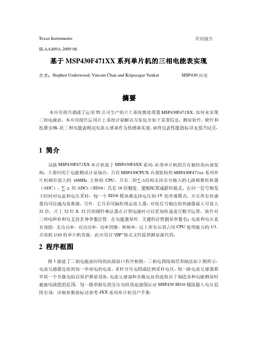
Texax Instruments 应用报告 SLAA409A-2009 06基于MSP430F471XX 系列系列单片机的三相电能单片机的三相电能单片机的三相电能表表实现作者:Stephen Underwood, Vincent Chan and Kripasagar Venkat MSP430应用摘要本应用报告描述了运用TI 公司生产的片上系统微处理器MSP430F471XX ,如何来实现三相电能表。
本应用报告运用片上系统计量解决方案包含如下重要信息:测量软件、硬件和校准步骤。
此三相电能表利用电流互感器作为传感器实现,最终仪表性能指标详见报告尾页。
1 简介这款MSP430F471XX 单片机属于MSP430F4XX 系列。
此类单片机因具有独特的内部架构,主要应用于电能测试计量场合。
具有MSP430CPUX 内部架构的MSP430F471xx 系列单片机拥有强大的16MHz 主频的CPU 。
具有二阶∑-∆结构支持差分输入的七路模数转换器(ADC )。
∑-∆ 的ADCs (SD16)具有16位精度,能够配置成群组模式,在同一信号触发下同时对电流和电压采样。
每一个SD16模块都支持电压到-1V 的普通模式,并且所有传感器均可以地为基准源。
另外,它具有可编程增益放大器,对低信号输出的传感器最大可放大32倍。
片上32位X 32位的硬件乘法器在计算电能时可以更加快速进行数学运算。
软件对三相电和单相电支持多种参数计算,在电能测量时,关键的计算测量参数有:电流和电压真有效值、无功功率、有功功率、功率因数、和频率。
以上所有运算占用CPU 处理能力的1/3,并消耗1/10的单片机资源。
此应用以“ZIP”格式文件提供测量源代码。
2 程序程序框图框图图1描述了三相电能表应用的高级接口程序框图。
三相电四线制星形接法如下图所示。
电流互感器连接到每一单相电的电流,采样分压电阻成比例采样电压。
每一路电流互感器都串联一个负载电阻以保护测量设备。
WJ159模块说明书

1路差分光栅尺磁栅尺编码器4倍频脉冲计数器,Modbus RTU模块WJ159产品特点:●差分光栅尺磁栅尺转换成标准Modbus RTU协议●可用作量程角度或者速度测量●采用4倍频计数,可识别正反转●测量值支持断电自动保存●可设置脉冲倍率自动换算实际值●模块可以输出5V的电源给光栅尺供电●脉冲输入有干扰时可以设置滤波时间●通过RS-485接口可以清零和设置测量值●宽电源供电范围:8~32VDC●可靠性高,编程方便,易于应用●标准DIN35导轨安装,方便集中布线●用户可编程设置模块地址、波特率等典型应用:●差分光栅尺脉冲信号测量●差分磁栅尺脉冲信号测量●三坐标系统位置测量●球栅尺脉冲信号测量图1WJ159模块外观图●光栅尺信号远传到工控机●编码器信号远传到工控机●编码器脉冲信号测量●智能工厂与工业物联网产品概述:WJ159产品实现传感器和主机之间的信号采集,用来解码光栅尺磁栅尺信号。
WJ159系列产品可应用在RS-485总线工业自动化控制系统,自动化机床,工业机器人,三坐标定位系统,位移测量,行程测量,角度测量,转速测量,产品计米等等。
产品包括信号采集,脉冲信号捕捉,信号转换和RS-485串行通信。
每个串口最多可接255只WJ159系列模块,通讯方式采用ASCII码通讯协议或MODBUS RTU通讯协议,波特率可由代码设置,能与其他厂家的控制模块挂在同一RS-485总线上,便于计算机编程。
图2WJ159模块内部框图WJ159系列产品是基于单片机的智能监测和控制系统,所有的用户设定的地址,波特率,数据格式,校验和状态等配置信息都储存在非易失性存储器EEPROM里。
WJ159系列产品按工业标准设计、制造,信号输入/输出之间不隔离,抗干扰能力强,可靠性高。
工作温度范围-45℃~+85℃。
功能简介:WJ159远程I/O模块,可以用来测量1路5V差分光栅尺磁栅尺编码器信号。
1、信号输入1路5V差分光栅尺磁栅尺编码器信号输入。
PLS159资料
周立功单片机 MP157数据手册(中文)-V1.00

ቤተ መጻሕፍቲ ባይዱ目 录
MP157:功率范围扩展的最小体积的高能效离线稳压器 · · · · · · · · · · · · · · · · · · · · · · · · · · · · · · · · · · · · ·1
1.1 1.2 1.3 1.4 1.5 1.6 1.7 1.8 1.9 1.10 1.11 1.12 1.13 1.14 描述· · · · · · · · · · · · · · · · · · · · · · · · · · · · · · · · · · · · · · · · · · · · · · · · · · · · · · · · · · · · · · · · · · · · · · · · · · · · · · · · · · · · · · · · · · · · · · · · · · ·1 特性· · · · · · · · · · · · · · · · · · · · · · · · · · · · · · · · · · · · · · · · · · · · · · · · · · · · · · · · · · · · · · · · · · · · · · · · · · · · · · · · · · · · · · · · · · · · · · · · · · ·1 应用· · · · · · · · · · · · · · · · · · · · · · · · · · · · · · · · · · · · · · · · · · · · · · · · · · · · · · · · · · · · · · · · · · · · · · · · · · · · · · · · · · · · · · · · · · · · · · · · · · ·1 典型应用· · · · · · ·
MP1593规格书

TEMPERATURE (°C)
Soft-Start Waveforms
TYPICAL APPLICATION
INPUT 4.75V to 28V
2 IN 7 EN 8 1 BS 3 SW
C5 10nF
100 95
Efficiency vs Load Current
VIN = 9V VIN = 24V VIN = 12V
OUTPUT 3.3V 3A
90
EFFICIENCY (%)
θJA
θJC
For Tape & Reel, add suffix –Z (eg. MP1593DN–Z) For RoHS Compliant Packaging, add suffix –LF (eg. MP1593DN–LF–Z)
ELECTRICAL CHARACTERISTICS
VIN = 12V, TA = +25°C, unless otherwise noted.
Parameter Shutdown Supply Current Supply Current Feedback Voltage Error Amplifier Voltage Gain Error Amplifier Transconductance High-Side Switch On-Resistance Low-Side Switch On-Resistance High-Side Switch Leakage Current Current Limit Current Sense to COMP Transconductance Oscillation Frequency Short Circuit Oscillation Frequency Maximum Duty Cycle Minimum Duty Cycle Symbol Condition VEN = 0V VEN = 2.6V, VFB = 1.4V VFB AEA GEA RDS(ON)1 RDS(ON)2 VEN = 0V, VSW = 0V 4.8 GCS fOSC1 fOSC2 DMAX DMIN VFB = 0V VFB = 1.0V VFB = 1.5V 335 25 ∆ICOMP = ±10µA 500 4.75V ≤ VIN ≤ 28V VCOMP < 2V Min Typ 20 1.0 1.222 400 800 100 10 0 6.2 5.4 385 45 90 0 435 60 10 7.6 1120 140 Max 30 1.2 1.250 Units µA mA V V/V µA/V mΩ Ω µA A A/V KHz KHz % %
- 1、下载文档前请自行甄别文档内容的完整性,平台不提供额外的编辑、内容补充、找答案等附加服务。
- 2、"仅部分预览"的文档,不可在线预览部分如存在完整性等问题,可反馈申请退款(可完整预览的文档不适用该条件!)。
- 3、如文档侵犯您的权益,请联系客服反馈,我们会尽快为您处理(人工客服工作时间:9:00-18:30)。
MP15912A, 32V, 330KHz Step-Down ConverterThe Future of Analog IC TechnologyDESCRIPTIONThe MP1591 is a high voltage step-down converter ideal for automotive power adapter battery chargers. Its wide 6.5V to 32V input voltage range covers the automotive battery’s requirements and it achieves 2A continuous output for quick charge capability.Current mode operation provides fast transient response and eases loop stabilization. Fault protection includes cycle-by-cycle current limiting and thermal shutdown. In shutdown mode, the converter draws only 20µA of supply current.The MP1591 requires a minimum number of readily available external components to complete a 2A step-down DC to DC converter solution.EVALUATION BOARD REFERENCEBoard NumberDimensions EV00202.1”X x 1.4”Y x 0.5”ZFEATURES• Wide 6.5V to 32V Input Operating Range • 34V Absolute Maximum Input • 2A Output Current• 120m Ω Internal Power MOSFET Switch• Stable with Low ESR Output CeramicCapacitors• Up to 95% Efficiency • 20µA Shutdown Mode • Fixed 330KHz Frequency • Thermal Shutdown• Cycle-by-Cycle Over Current Protection • Output Adjustable From 1.23V to 21V • Under Voltage Lockout • Reference Voltage Output• Available in 8-Pin SOIC PackagesAPPLICATIONS• Automotive Power Adapters• PDA and Cellular Phone Battery Chargers • Distributed Power Systems • Automotive Aftermarket Electronics“MPS” and “The Future of Analog IC Technology” are Registered Trademarks of Monolithic Power Systems, Inc.TYPICAL APPLICATIONC21009080706050403020E F F I C I E N C Y (%)0.51 1.52LOAD CURRENT (A)Efficiency vs Load CurrentMP1591 – 2A, 32V, 330KHz STEP-DOWN CONVERTERPACKAGE REFERENCE* For Tape & Reel, add suffix –Z (eg. MP1591DN–Z) For RoHS Compliant Packaging, add suffix –LF(eg. MP1591DN–LF–Z) ABSOLUTE MAXIMUM RATINGS (1) IN Supply Voltage........................–0.3V to +34V SW Voltage.............................–1V to V IN + 0.3V BS Voltage....................V SW – 0.3V to V SW + 6V All Other Pins.................................–0.3V to +6V Junction Temperature...............................150°C Lead Temperature....................................260°C Storage Temperature..............–65°C to +150°C Recommended Operating Conditions (2) Input Voltage...................................6.5V to 32V Operating Temperature.............–40°C to +85°C Thermal Resistance (3)θJA θJCSOIC8 (w/ Exposed Pad).......50......10...°C/W SOIC8.....................................90......45...°C/W Notes:1) Exceeding these ratings may damage the device.2) The device is not guaranteed to function outside of itsoperating conditions.3) Measured on approximately 1” square of 1 oz copper.ELECTRICAL CHARACTERISTICSV IN = 12V, T A = +25°C, unless otherwise noted.Parameter Symbol ConditionMinTypMaxUnits Shutdown Supply Current V EN= 0V 20 35 µASupply Current V EN = 5V, V FB = 1.4V 1.0 1.2 mAFeedback Voltage 6.5V ≤ V IN≤ 32V, V COMP < 2V 1.202 1.230 1.258VError Amplifier Voltage Gain 400 V/VError Amplifier Transconductance ∆I C = ±10µA 500 700 1100 µA/VHigh-Side Switch On Resistance (4) 120 mΩLow-Side Switch On Resistance (4)8.5 ΩHigh-Side Switch Leakage Current V EN = 0V, V SW = 0V 0 10 µACurrent Limit (5) 2.53.64.9A Current Sense to COMPTransconductance3.5 A/VOscillation Frequency 280 330 380 KHzShort Circuit Oscillation Frequency V FB = 0V 35 KHzMaximum Duty Cycle (4)V FB = 1.0V 90 %Minimum Duty Cycle (4)V FB = 1.5V 0 %EN Shutdown Threshold Voltage 0.8 1.2 1.6 VEnable Pull-Up Current V EN = 0V 1.8 µAEN UVLO Threshold V EN Rising 2.4 2.6 2.8 VEN UVLO Threshold Hysteresis 250 mVMP1591 – 2A, 32V, 330KHz STEP-DOWN CONVERTERELECTRICAL CHARACTERISTICS (continued)V IN = 12V, T A = +25°C, unless otherwise noted.MaxUnitsMinTypParameter Symbol ConditionThermal Shutdown (4) 160 °CREF Voltage I REF = 0 5.0 VREF Load Regulation (4)∆I REF = 0 to 1mA 100 mVREF Line Regulation (4)I REF = 100µA, V IN = 6.5 to 32V 30 mVNotes:4) These parameters are guaranteed by design, not production tested.5) Equivalent output current = 1.5A ≥ 50% Duty Cycle≤ 50% Duty Cycle2.0AAssumes ripple current = 30% of load current.Slope compensation changes current limit.PIN FUNCTIONSPin # Name Description1 BS High-Side Gate Drive Boost Input. BS supplies the drive for the high-side N-Channel MOSFETswitch. Connect a 10nF or greater capacitor from SW to BS to power the high-side switch.2 IN Power Input. IN supplies the power to the IC, as well as the step-down converter switches.Drive IN with a 6.5V to 32V power source. Bypass IN to GND with a suitably large capacitor toeliminate noise on the input to the IC. See Input Capacitor.3 SW Power Switching Output. SW is the switching node that supplies power to the output. Connectthe output LC filter from SW to the output load. Note that a capacitor is required from SW to BSto power the high-side switch.4 GND Ground. For the MP1591DN, connect the Exposed Pad to pin 4.5 FB Feedback Input. FB senses the output voltage to regulate that voltage. Drive FB with a resistivevoltage divider from the output voltage. The feedback threshold is 1.230V. See Setting theOutput Voltage.6 COMP Compensation Node. COMP is used to compensate the regulation control loop. Connect aseries RC network from COMP to GND to compensate the regulation control loop. In somecases, an additional capacitor from COMP to GND is required. See Compensation.7 EN Enable/UVLO. A voltage greater than 2.8V enables operation. For complete low currentshutdown the EN pin voltage needs to be less than 800mV.8 REF Reference Output. REF is the 5V reference voltage output. It can supply up to 1mA to externalcircuitry. If used, bypass REF to GND with 10nF or greater capacitor. Leave REF unconnectedif not used.MP1591 – 2A, 32V, 330KHz STEP-DOWN CONVERTEROPERATIONThe MP1591 is a current mode step-down regulator. It regulates input voltages from 6.5V to 32V down to an output voltage as low as 1.230V and is able to supply up to 2A of load current.The MP1591 uses current-mode control to regulate the output voltage. The output voltage is measured at FB through a resistive voltage divider and amplified through the internal error amplifier. The output current of the transconductance error amplifier is presented at COMP where a network compensates the regulation control system.The voltage at COMP is compared to the switch current measured internally to control the output voltage. The converter uses an internal N-Channel MOSFET switch to step-down the input voltage to the regulated output voltage. Since the MOSFET requires a gate voltage greater than the input voltage, a boost capacitor connected between SW and BS drives the gate. The capacitor is internally charged while SW is low. An internal 10Ω switch from SW to GND is used to insure that SW is pulled to GND when the switch is off to fully charge the BS capacitorCOMPIN EN GNDSWBSREF FBFigure 1—Functional Block DiagramMP1591 – 2A, 32V, 330KHz STEP-DOWN CONVERTERAPPLICATION INFORMATIONCOMPONENT SELECTIONSetting the Output VoltageThe output voltage is set using a resistive voltage divider from the output voltage to FB. The voltage divider divides the output voltage down by the ratio:)2R 1R (2R V V OUT FB +×=Where V FB is the feedback voltage and V OUT isthe output voltage. Thus the output voltage is:2R )2R 1R (230.1V OUT +×= A typical value for R2 can be as high as 100k Ω, but 10k Ω is recommended. Using that value, R1 is determined by:)230.1V (18.81R OUT −×≅For example, for a 3.3V output voltage, R2 is 10k Ω, and R1 is 17k Ω.Inductor (L1)The inductor is required to supply constant current to the output load while being driven by the switched input voltage. A larger value inductor results in less ripple current that results in lower output ripple voltage. However, the larger value inductor has a larger physical size, higher series resistance, and/or lower saturation current. Choose an inductor that does not saturate under the worst-case load conditions. A good rule to use for determining the inductance is to allow the peak-to-peak ripple current in the inductor to be approximately 30% of the maximum load current that the IC can provide. Also, make sure that the peak inductor current (the load current plus half the peak-to-peak inductor ripple current) is below the 2.3A minimum current limit.The inductance value can be calculated by the equation:)I f V ()V V (V 1L IN OUT IN OUT ∆××−×=Where V IN is the input voltage, f is the switching frequency and ∆I is the peak-to-peak inductor ripple current.Table 1 lists a number of suitable inductors from various manufacturers.Table 1—Inductor Selection GuidePackage Dimensions(mm) Vendor/ Model Core Type CoreMaterial W L H SumidaCR75 Open Ferrite 7.0 7.8 5.5 CDH74 Open Ferrite 7.3 8.0 5.2 CDRH5D28Shielded Ferrite 5.5 5.7 5.5 CDRH5D28Shielded Ferrite 5.5 5.7 5.5 CDRH6D28Shielded Ferrite 6.7 6.7 3.0 CDRH104R Shielded Ferrite 10.110.0 3.0Toko D53LC Type AShieldedFerrite 5.0 5.0 3.0 D75C Shielded Ferrite 7.6 7.6 5.1 D104C Shielded Ferrite 10.010.0 4.3 D10FL Open Ferrite 9.7 1.5 4.0 CoilcraftDO3308 Open Ferrite 9.4 13.0 3.0 DO3316 Open Ferrite 9.4 13.0 5.1Input Capacitor (C1)The input current to the step-down converter is discontinuous, and so a capacitor is required to supply the AC current to the step-down converter while maintaining the DC input voltage. A low ESR capacitor is required to keep the noise at the IC to a minimum. Ceramic capacitors are preferred, but tantalum or low ESR electrolytic capacitors may also suffice.MP1591 – 2A, 32V, 330KHz STEP-DOWN CONVERTERThe input capacitor value should be greater than 10µF. The capacitor can be electrolytic, tantalum or ceramic. However, since it absorbs the input switching current it requires an adequate ripple current rating. Its RMS current rating should be greater than approximately 1/2 of the DC load current.For insuring stable operation C1 should be placed as close to the IC as possible. Alternately, a smaller high quality ceramic 0.1µF capacitor may be placed closer to the IC and a larger capacitor placed farther away. If using this technique, it is recommended that the larger capacitor be a tantalum or electrolytic type. All ceramic capacitors should be placed close to the MP1591.Output Capacitor (C5)The output capacitor is required to maintain the DC output voltage. Low ESR capacitors are preferred to keep the output voltage ripple low. The characteristics of the output capacitor also affect the stability of the regulation control system. Ceramic, tantalum or low ESR electrolytic capacitors are recommended. In the case of ceramic capacitors, the impedance at the switching frequency is dominated by the capacitance, and so the output voltage ripple is mostly independent of the ESR. The output voltage ripple is estimated to be:2SWLCIN RIPPLE ff V 4.1V ⎟⎟⎠⎞⎜⎜⎝⎛××≅ Where V RIPPLE is the output ripple voltage, f LC isthe resonant frequency of the LC filter, f SW is the switching frequency.In the case of tantalum or low-ESR electrolytic capacitors, the ESR dominates the impedance at the switching frequency, and so the output ripple is calculated as:ESR RIPPLE R I V ×∆≅Where V RIPPLE is the output voltage ripple and R ESR is the equivalent series resistance of the output capacitors.Output Rectifier Diode (D1)The output rectifier diode supplies the current to the inductor when the high-side switch is off. To reduce losses due to the diode forward voltage and recovery times, use a Schottky rectifier. Table 2 provides some recommended Schottky rectifiers based on the maximum input voltage and current rating.Table 2—Diode Selection Guide2A Load Current 3A Load Current V IN (Max)Part Number Vendor PartNumberVendor15V 30BQ15 4B220 1 B320 1SK23 6 SK33 1, 620V SR22 6 SS32 3 20BQ030 4 B330 1 B230 1 B340L 1SK23 6 MBRD330 4, 5SR23 3, 6 SK33 1, 6 30V SS23 2, 3 SS33 2, 3 21DQ04 4 B340L 1 MBRS240L 5 MBRS340 4SK24 6 SK34 1, 6 34VSS24 2, 3 SS34 2, 3Table 3 lists manufacturer’s websites.Table 3—Schottky Diode Manufacturers# Vendor Web Site 1 Diodes, Inc.2 Fairchild Semiconductor 3 General Semiconductor 4 International Rectifier 5 On Semiconductor 6 Pan Jit InternationalChoose a rectifier whose maximum reverse voltage rating is greater than the maximum input voltage, and whose current rating is greater than the maximum load current.MP1591 – 2A, 32V, 330KHz STEP-DOWN CONVERTERCompensationThe system stability is controlled through the COMP pin. COMP is the output of the internal transconductance error amplifier. A series capacitor-resistor combination sets a pole-zero combination to control the characteristics of the control system. The DC loop gain is:LOAD CS VEA OUTREFVDC R G A V V A ×××=Where V REF is the feedback threshold voltage, 1.230V, A VEA is the transconductance error amplifier voltage gain, 400 V/V, and G CS is the current sense gain (roughly the output current divided by the voltage at COMP), 3.5 A/V. The system has 2 poles of importance; one is due to the compensation capacitor (C4) and the other is due to the output capacitor (C5). These are:)4C A 2(G f VEA MEA1P ××π=Where f P1 is the first pole, and G MEA is the error amplifier transconductance (770µS) and)5C R 2(1f LOAD 2P ××π=The system has one zero of importance due to the compensation capacitor (C4) and the compensation resistor (R3) which is)4C 3R 2(1f 1Z ××π=If large value capacitors with relatively high equivalent-series-resistance (ESR) are used, the zero due to the capacitance and ESR of the output capacitor can be compensated by a third pole set by R3 and C3)3C 3R 2(1f 3P ××π=The system crossover frequency f C, (the frequency where the loop gain drops to 1, or 0dB) is important. A good rule of thumb is to set the crossover frequency to approximately one tenth of the switching frequency. In this case, the switching frequency is 330KHz, so use a crossover frequency of 33KHz. Lower crossover frequencies result in slower response and worse transient load recovery. Higher crossover frequencies can result in instability. Choosing the Compensation Components The values of the compensation components given in Table 4 yield a stable control loop for the output voltage and given capacitor. Table 4—Compensation Values for Typical Output Voltage/Capacitor CombinationsV OUT C5R3 C3 C42.5V 22µF Ceramic3.9k Ω None4.7nF 3.3V 22µF Ceramic5.1k Ω None 3.9nF 5V 22µF Ceramic 7.5k Ω None 2.7nF 12V 22µF Ceramic 18k Ω None 1.2nF 2.5V 47µF SP-Cap 8.2k Ω None 2.2nF 3.3V 47µF SP-Cap 10k Ω None 2.2nF 5V 47µF SP-Cap 16k Ω None 1.5nF 12V 47µF SP-Cap 36k Ω None 1nF 2.5V 560µF/6.3V, AL30m Ω ESR 100k Ω 150pF 1nF 3.3V 560µF/6.3V, AL 30m Ω ESR 120k Ω 120pF 1nF 5V 470µF/10V, AL 30m Ω ESR 150k Ω 82pF 1nF 12V220µF/25V, AL 30m Ω ESR180k Ω 33pF 1nFNote: “AL” = ElectrolyticMP1591 – 2A, 32V, 330KHz STEP-DOWN CONVERTERTo optimize the compensation components that are not listed in Table 4, use the following procedure.Choose the compensation resistor to set the desired crossover frequency. Determine the value by the following equation:REFCS EA COUT V G G f V 5C 23R ×××××π=Putting in the know constants and setting the crossover frequency to the desired 33KHz:OUT 7V 5C 1088.63R ×××≅Choose the compensation capacitor to set the zero below one fourth of the crossover frequency. Determine the value by the following equation:3R 1093.1f 3R 24C 5C−×≈××π> Determine if the second compensationcapacitor, C3, is required. It is required if the ESR zero of the output capacitor occurs at less than four times the crossover frequency, or1f R 5C 8C ESR ≥×××πIf this is the case, then add the second compensation resistor. Determine the value by the equation:3R R 5C 3C )MAX (ESR ×=Where R ESR(MAX)is the maximum ESR of the output capacitor.Example:V OUT = 5V, C5 = 22µF Ceramic (ESR = 10m Ω)R3 ≈ 6.88x10⁷ (22x10-6) (5) = 7568Ω Use the nearest standard value of 7.5k Ω.C4 > 1.93x10⁻⁵ / 7.5K = 2.57nFUse standard value of 2.7nF.8π x C5 x R ESR x f C = 0.22, which is less than 1. Therefore, no second compensation capacitor (C3) is required.External Bootstrap DiodeIt is recommended that an external bootstrap diode be added when the system has a 5V fixed input or the power supply generates a 5V output. This helps improve the efficiency of the regulator. The bootstrap diode can be a low cost one such as IN4148 or BAT54.10nFFigure 2—External Bootstrap Diode This diode is also recommended for high duty cycle operation (whenINOUTV V >65%) and high output voltage (V OUT >12V) applications.MP1591 – 2A, 32V, 330KHz STEP-DOWN CONVERTERTYPICAL APPLICATION CIRCUITSC2Figure 3—MP1591 with Murata 22µF / 10V Ceramic Output CapacitorC2Figure 4—MP1591 with Panasonic 47µF / 6.3V Special Polymer Output CapacitorMP1591 – 2A, 32V, 330KHz STEP-DOWN CONVERTERPACKAGE INFORMATIONSOIC8DETAIL "A" 5) DRAWING CONFORMS TO JEDEC MS-012, VARIATION AA.6) DRAWING IS NOT TO SCALE.MP1591 – 2A, 32V, 330KHz STEP-DOWN CONVERTERNOTICE: The information in this document is subject to change without notice. Users should warrant and guarantee that thirdparty Intellectual Property rights are not infringed upon when integrating MPS products into any application. MPS will not assume any legal responsibility for any said applications.MP1591 Rev. 2.3 119/27/2006 MPS Proprietary Information. Unauthorized Photocopy and Duplication Prohibited.© 2006 MPS. All Rights Reserved.SOIC8E (WITH EXPOSED PAD)TOP VIEW FRONT VIEWBOTTOM VIEWNOTE:1) CONTROL DIMENSION IS IN INCHES. DIMENSION IN BRACKET IS IN MILLIMETERS.2) PACKAGE LENGTH DOES NOT INCLUDE MOLD FLASH, PROTRUSIONS OR GATE BURRS.3) PACKAGE WIDTH DOES NOT INCLUDE INTERLEAD FLASH OR PROTRUSIONS.4) LEAD COPLANARITY (BOTTOM OF LEADS AFTER FORMING) SHALL BE 0.004" INCHES MAX.5) DRAWING CONFORMS TO JEDEC MS-012, VARIATION BA.6) DRAWING IS NOT TO SCALE.RECOMMENDED LAND PATTERNPIN 1 IDDETAIL "A"o元器件交易网。