TPS65140
TPS是什么

4
- 3
11
送Jetta完成品
4 3
5
车外园
換加工完了品起动,取加工完了品
8
110 3
6
滚齿
換加工完了品起动,取加工完了品
6
110 2
7
完成台
送完成品
4
-
工序能力分析
动力齿轮线各岗位山积表(改善前)
工艺节拍" 200 190 180 170 160 150 140 130 120 110 100 90 80 70 60 50 40 30 20 10 0 实际节拍"
工 序 名
010、020/ 010、020/ 010
毛坯台取毛坯 取毛坯 插齿 換加工完了品起动 , 取加工完了品 插齿 換加工完了品起动 , 取加工完了品 剃齿 換加工完成品起动 , 取毛坯
3 3
3 2 2 41” 要改善時間
8 8 6
130 2 130 3 40 3 40 3 - 3
換加工完成品起动 , 取加工完成品2 个 6 完成台送Jetta完成品, 取毛坯 送Jetta完成品 车外园換加工完了品起动 , 取加工完了品 滚齿 換加工完了品起动 , 取加工完了品 完成台 送完成品 4 4
插齿机 插齿机 剔齿机 清洗机 打印机 感应淬火机 手动校直机 数控外圆磨床 端面外圆磨床 数控车床 数控车床 专机 立式加工中心 磁力探伤机 清洗机
8 8 6 8 4 6 60 8 6 5 5 7 15 15 8
10 10 40 12 26 31 —— 55 30 —— 55 16 15 19 12
最终目的:质量稳定、成本降低、效率 提升。
不要求全责备,能做多少做多少.不怕慢, 就怕站!
TPS40210DGQ中文数据手册

输入电源 V VDD
输入电压范围
TPS40211
IVDD
工作电流
欠压分离
V UVLO( on)
开启阈值电压
V UVLO( hyst)
UVLO滞后
OSCILLATOR
振荡器的频率范围.
(1)
fOSC
振荡器频率
频率线路调整
V SLP PWM
斜率补偿斜坡
tON(min)
最小脉冲宽度
tOFF(min)
最小关断时间
MAX UNIT
4..2
5.6
7.2 V / V
1
3 µA
375
400
330
400
毫安
7
8
9V
0.7
1.3
V
25
130
220 毫伏
0.7
1.1
1.5 MΩ
4
提交文档反馈
产品文件夹链接(s): TPS40210 TPS40211
Copyright © 2008, Texas Instruments Incorporated
V VDD = 12V (1) V VDD = 30V
V FB = 0.6 V, V COMP = 1 V V FB = 1.2 V, V COMP = 1 V
V ISNS( oc) DOC V SS( r st) TBLNK
过电流检测阈值(在 ISNS针)
过电流占空比
(1)
过电流复位阈值电压( SS引脚)
前沿消隐
(1)
4.5 ≤ VDD
≤ TJ ≤ 125°C
(1) 由设计保证.未经生产测试了.
TPS40210, TPS40211
TPS650250RHBT;TPS650250RHBR;TPS650250EVM-447;中文规格书,Datasheet资料

FEATURESAPPLICATIONSDESCRIPTIONTPS650250/2.8V V /1.8V m FF F TPS650250 SLVS843–DECEMBER 2008Power Management IC for Li-Ion Powered SystemsThe TPS650250also integrates two general purpose 200mA LDO voltage regulators,which are enabled •1.6A,97%Efficient Step-Down Converter for with an external input pin.Each LDO operates with System Voltage (VDCDC1)an input voltage range between 1.5V and 6.5V – 3.3V or2.8V or Adjustableallowing them to be supplied from one of the step-down converters or directly from the battery.The •0.8A,up to 95%Efficient Step-Down Converter output voltage of the LDOs can be set with an for Memory Voltage (VDCDC2)external resistor divider for maximum flexibility.– 1.8V or 2.5V or AdjustableAdditionally there is a 30mA LDO typically used to •0.8A,90%Efficient Step-Down Converter for provide power in a processor based system to a Processor Core (VDCDC3)voltage rail that is always on.TPS650250comes in a small 5mm x 5mm 32pin QFN package (RHB).•adjustable output voltage on VDCDC3•30mA LDO for Vdd_aliveFunctional Block Diagram•2×200mA General Purpose LDOs (LDO1and LDO2)•Dynamic Voltage Management for Processor Core•LDO1and LDO2Voltage Externally Adjustable •Separate Enable Pins for Inductive Converters • 2.25MHz Switching Frequency •85µA Quiescent Current•Thermal Shutdown Protection•Cellular/Smart Phone •GPS•Digital Still Camera•Split Supply DSP and µP Solutions •Samsung ARM-Based Processors,etc.The TPS650250is an integrated Power Management IC for applications powered by one Li-Ion or Li-Polymer cell,which require multiple power rails.The TPS650250provides three highly efficient,step-down converters targeted at providing the core voltage,peripheral,I/O and memory rails in a processor based system.All three step-down converters enter a low power mode at light load for maximum efficiency across the widest possible range of load currents.The converters can be forced into fixed frequency PWM mode by pulling the MODE pin high.Please be aware that an important notice concerning availability,standard warranty,and use in critical applications of Texas Instruments semiconductor products and disclaimers thereto appears at the end of this data sheet.PRODUCTION DATA information is current as of publication date.Copyright ©2008,Texas Instruments IncorporatedProducts conform to specifications per the terms of the Texas Instruments standard warranty.Production processing does not necessarily include testing of all parameters.ht t p ://oABSOLUTE MAXIMUM RATINGSDISSIPATION RATINGSTPS650250SLVS843–DECEMBER These devices have limited built-in ESD protection.The leads should be shorted together or the device placed in conductive foam during storage or handling to prevent electrostatic damage to the MOS gates.ORDERING INFORMATION (1)VOLTAGE ATOUTPUT CURRENT ON VOLTAGE AT T APACKAGE PART NUMBER (2)DCDC3DCDC1/DCDC2/DCDC3VDD_ALIVE32Pin QFN –40°C to 85°C Adjustable1.6A /0.8A /0.8A1VTPS650250RHB(RHB)(1)For the most current package and ordering information,see the Package Option Addendum at the end of this document,or see the TI website at .(2)The RHB package is available in tape and reel.Add R suffix (TPS650250RHBR)to order quantities of 3000parts per reel.Add T suffix (TPS650250RHBT)to order quantities of 250parts per reel.over operating free-air temperature range (unless otherwise noted)(1)VALUEUNIT Input voltage range on all pins except A/PGND pins with respect to AGND –0.3to 7V Voltage range on pins VLDO1,VLDO2,FB_LDO1,FB_LDO2–0.3to 3.6V Current at VINDCDC1,L1,PGND1,VINDCDC2,L2,PGND2,VINDCDC3,L3,PGND32000mA Peak current at all other pins 500mA Continuous total power dissipation See Dissipation Rating TableT A Operating free-air temperature –40to 85°C T J Maximum junction temperature 125°C T st Storage temperature–65to 150°C(1)Stresses beyond those listed under absolute maximum ratings may cause permanent damage to the device.These are stress ratings only and functional operation of the device at these or any other conditions beyond those indicated under recommended operating conditions is not implied.Exposure to absolute-maximum-rated conditions for extended periods may affect device reliability.T A ≤25°C DERATING FACTOR T A =70°C T A =85°C PACKAGE (1)R θJA POWER RATINGABOVE T A =25°CPOWER RATINGPOWER RATINGRHB35K/W2.85W28mW/K1.57W1.14W(1)The thermal resistance junction to ambient of the RHB package is measured on a high K board.The thermal resistance junction to power pad is 1.5k/W.2Submit Documentation FeedbackCopyright ©2008,Texas Instruments IncorporatedProduct Folder Link(s):TPS650250ht t p ://oRECOMMENDED OPERATING CONDITIONS TPS650250 SLVS843–DECEMBER2008MIN NOM MAX UNIT V CC Input voltage range step-down converters,VINDCDC1,VINDCDC2,VINDCDC3 2.5 6.0V Output voltage range for step-down converter,VDCDC1(1)0.6VINDCDC1V V O Output voltage range for mem step-down converter,VDCDC2(1)0.6VINDCDC2V Output voltage range for core step-down converter,VDCDC30.6VINDCDC3V V I Input voltage range for LDOs,VINLDO1,VINLDO2 1.5 6.5V V O Output voltage range for LDOs1 3.3VI O Output current at L,V1DCDC11600mAL1Inductor at L1(2) 1.5 2.2µHC I Input capacitor at VINDCDC1(2)10µFC O Output capacitor at VDCDC1(2)1022µFI O Output current at L2,VDCDC2800mAL2Inductor at L2(2) 1.5 2.2µHC I Input capacitor at VINDCDC2(2)10µFC O Output capacitor at VDCDC2(2)1022µFI O Output current at L3,VDCDC3800mAL3Inductor at L3(2) 1.5 2.2µHC I Input capacitor at VINDCDC3(2)10µFC O Output capacitor at VDCDC3(2)1022µFC I Input capacitor at VCC(2)1µFC I Input capacitor at VINLDO(2)1µFC O Output capacitor at VLDO1,VLDO2(2) 2.2µFI O Output current at VLDO1,VLDO2200mAC O Output capacitor at Vdd_alive(2) 2.2µFI O Output current at Vdd_alive30mAT A Operating ambient temperature–4085°C T J Operating junction temperature–40125°C R CC Resistor from VINDCDC3,VINDCDC2,VINDCDC1to V CC used for filtering(3)110Ω(1)When using an external resistor divider at DEFDCDC2,DEFDCDC1.(2)See applications section for more information,for V O>2.85V choose3.3µH inductor.(3)Up to2.5mA can flow into V CC when all3converters are running in PWM,this resistor will cause the UVLO threshold to be shiftedaccordingly.Copyright©2008,Texas Instruments Incorporated Submit Documentation Feedback3Product Folder Link(s):TPS650250h t t p://oELECTRICAL CHARACTERISTICSTPS650250SLVS843–DECEMBER VINDCDC1=VINDCDC2=VINDCDC3=VCC =VINLDO =3.6V,T A =–40°C to 85°C,typical values are at T A =25°C (unless otherwise noted)CONTROL SIGNALS:EN_DCDC1,EN_DCDC2,EN_DCDC3,EN_LDO,MODE,EN_VDD_ALIVEPARAMETERTEST CONDITIONSMIN TYPMAX UNIT High level input V IH 1.45VCC V voltage Low level input V IL 00.4V voltageI HInput bias current0.010.1µASUPPLY PINS:VCC,VINDCDC1,VINDCDC2,VINDCDC3PFM All 3DCDC converters enabled,zero load 135170and no switching,LDOs enabledPFM All 3DCDC converters enabled,zero load and no switching,LDO1,LDO2=OFF,Vdd_alive 75100=ONOperating quiescent I (qPFM)V CC =3.6VµAcurrentPFM DCDC1and DCDC2converters enabled,zero load and no switching,LDO1,LDO2=OFF,5580Vdd_alive =ONPFM DCDC1converter enabled,zero load and no 4060switching,LDO1,LDO2=OFF,Vdd_alive =ON All 3DCDC converters enabled &running in PWM,2LDOs offCurrent into V CC ;PWM DCDC1and DCDC2converters enabled and1.52.5I VCC(PWM)V CC =3.6VmAPWMrunning in PWM,LDOs offPWM DCDC1converter enabled and running in 0.852PWM,LDOs offAll converters disabled,LDO1,LDO2=OFF,16Vdd_alive =OFFI qQuiescent currentV CC =3.6VµAAll converters disabled,LDO1,LDO2=OFF,26Vdd_alive =ON4Submit Documentation FeedbackCopyright ©2008,Texas Instruments IncorporatedProduct Folder Link(s):TPS650250ht t p ://oELECTRICAL CHARACTERISTICS TPS650250 SLVS843–DECEMBER2008 VINDCDC1=VINDCDC2=VINDCDC3=VCC=VINLDO=3.6V,T A=–40°C to85°C,typical values are at T A=25°C(unless otherwise noted)PARAMETER TEST CONDITIONS MIN TYP MAX UNIT VDCDC1STEP-DOWN CONVERTERV I Input voltage range,VINDCDC1 2.56VI O Maximum output current V O=3.3V1600mAI SD Shutdown supply current in VINDCDC1EN_DCDC1=GND0.11µAR DS(on)P-channel MOSFET on-resistance VINDCDC1=VGS=3.6V125261mΩI LP P-channel leakage current VINDCDC1=6V2µAR DS(on)N-channel MOSFET on-resistance VINDCDC1=VGS=3.6V130260mΩI LN N-channel leakage current V DS=6V710µAI LIMF Forward current limit(P-and N-channel) 2.5V<V INMAIN<6V 1.75 1.97 2.15Af S Oscillator frequency 1.95 2.25 2.55MHzFixed output voltage 2.8V–2%2%VINDCDC1=3.3V to6V;MODE=0(PWM/PFM)0mA≤IO ≤1.0A3.3V–2%2% Fixed output voltage 2.8V–1%1%VINDCDC1=3.7V to6V;MODE=1(PWM)0mA≤IO ≤1.0A3.3V–1%1%VDCDC1Adjustable output voltage with resistorVINDCDC1=VDCDC1+0.4V(min2.5V)divider at DEFDCDC1MODE=0–2%2%to6V;0mA≤I O≤1.6A(PWM/PFM)Adjustable output voltage with resistorVINDCDC1=VDCDC1+0.4V(min2.5V)divider at DEFDCDC1;MODE=1–1%1%to6V;0mA≤I O≤1.6A(PWM)VINDCDC1=VDCDC1+0.3V(min.2.5V)Line regulation0%/Vto6V;I O=10mALoad regulation I O=10mA to1.6A0.25%/AVDCDC1ramping from5%to95%oft SS Soft start ramp time750µstarget valueR(L1)Internal resistance from L1to GND1MΩCopyright©2008,Texas Instruments Incorporated Submit Documentation Feedback5Product Folder Link(s):TPS650250h t t p://oELECTRICAL CHARACTERISTICSTPS650250SLVS843–DECEMBER VINDCDC1=VINDCDC2=VINDCDC3=VCC =VINLDO =3.6V,T A =–40°C to 85°C,typical values are at T A =25°C (unless otherwise noted)PARAMETERTEST CONDITIONSMINTYPMAXUNITVDCDC2STEP-DOWN CONVERTER V I Input voltage range,VINDCDC2 2.56V I O Maximum output currentV O =2.5V800mA I SD Shutdown supply current in VINDCDC2EN_DCDC2=GND 0.11µA R DS(on)P-channel MOSFET on-resistance VINDCDC2=V GS =3.6V 140300m ΩI LP P-channel leakage current VINDCDC2=6.0V 2µA R DS(on)N-channel MOSFET on-resistance VINDCDC2=VGS =3.6V 150297m ΩI LN N-channel leakage current V DS =6V710µA I LIMF Forward current limit (P-and N-channel) 2.5V <VINDCDC2<6V1.05 1.16 1.29A f SOscillator frequency 1.95 2.252.55MHz1.8V VINDCDC2=2.5V to 6V;0mA ≤I O ≤1.6A –2%2%Fixed output voltage MODE =0(PWM/PFM) 2.5V VINDCDC2=3V to 6V;0mA ≤I O ≤1.6A –2%2%1.8V VINDCDC2=2.5V to 6V;0mA ≤I O ≤1.6A –2%2%Fixed output voltage MODE =1(PWM)2.5VVINDCDC2=3V to 6V;0mA ≤I O ≤1.6A –1%1%VDCDC2Adjustable output voltage with resistor VINDCDC2=VDCDC2+0.5V (min 2.5V)divider at DEFDCDC2MODE =0–2%2%to 6V;0mA ≤I O ≤1.6A(PWM)Adjustable output voltage with resistor VINDCDC2=VDCDC2+0.5V (min 2.5V)divider at DEFDCDC2;MODE =1–1%1%to 6V;0mA ≤I O ≤1.6A(PWM)VINDCDC2=VDCDC2+0.3V (min.2.5Line regulation 0.0%/V V)to 6V;I O =10mA Load regulationI O =10mA to 1.6A0.25%/A VDCDC2ramping from 5%to 95%of t SS Soft start ramp time750µs target value R(L2)Internal resistance from L2to GND1M Ω6Submit Documentation FeedbackCopyright ©2008,Texas Instruments IncorporatedProduct Folder Link(s):TPS650250ht t p ://oELECTRICAL CHARACTERISTICS TPS650250 SLVS843–DECEMBER2008 VINDCDC1=VINDCDC2=VINDCDC3=VCC=VINLDO=3.6V,T A=–40°C to85°C,typical values are at T A=25°C(unless otherwise noted)PARAMETER TEST CONDITIONS MIN TYP MAX UNIT VDCDC3STEP-DOWN CONVERTERV I Input voltage range,VINDCDC3 2.5 6.0VI O Maximum output current V O=1.6V800mAShutdown supply current inI SD EN_DCDC3=GND0.11µAVINDCDC3R DS(on)P-channel MOSFET on-resistance V INDCDC3=V GS=3.6V310698mΩI LP P-channel leakage current VINDCDC3=6V0.12µAR DS(on)N-channel MOSFET on-resistance V INDCDC3=V GS=3.6V220503mΩI LN N-channel leakage current V DS=6.0V710µAForward current limit(P-andI LIMF 2.5V<V INDCDC3<6V 1.00 1.20 1.40AN-channel)f S Oscillator frequency 1.95 2.25 2.55MHzAdjustable output voltage with VINDCDC3=VDCDC3+0.5V(min2.5V)to6V;resistor divider at DEFDCDC20mA≤I O≤0.8A–2%2%MODE=0(PWM)VDCDC3Adjustable output voltage with VINDCDC3=VDCDC3+0.5V(min2.5V)to6V;resistor divider at DEFDCDC2;0mA≤I O≤0.8A–1%1%MODE=1(PWM)VINDCDC3=VDCDC3+0.3V(min.2.5V)toLine regulation0.0%/V6V;I O=10mALoad regulation I O=10mA to600mA0.25%/AVDCDC3ramping from5%to95%of targett SS Soft start ramp time750µsvalueR(L3)Internal resistance from L3to GND1MΩCopyright©2008,Texas Instruments Incorporated Submit Documentation Feedback7Product Folder Link(s):TPS650250h t t p://oELECTRICAL CHARACTERISTICSTPS650250SLVS843–DECEMBER VINDCDC1=VINDCDC2=VINDCDC3=VCC =VINLDO =3.6V,T A =–40°C to 85°C,typical values are at T A =25°C (unless otherwise noted)PARAMETERTEST CONDITIONSMIN TYP MAX UNIT VLDO1and VLDO2Low Dropout Regulators I (q)Operating quiescent current Current per LDO into VINLDO 1630µA I (SD)Shutdown currentTotal current into VINLDO,VLDO =0V0.62µA V I Input voltage range for LDO1,LDO2 1.5 6.5V V O LDO1output voltage range 1 3.3V LDO2output voltage range 13.3V VFB LDO1and LDO2feedback voltage See(1)1.0V I O Maximum output current for LDO1,LDO2V I =1.8V,V O =1.3V 200mA I O Maximum output current for LDO1,LDO2V I =1.5V;V O =1.3V 120mAI SCLDO1and LDO2short circuit current limit V LDO1=GND,V LDO2=GND 400mA Minimum voltage drop at LDO1,LDO2I O =50mA,VINLDO =1.8V 120mV Minimum voltage drop at LDO1,LDO2I O =50mA,VINLDO =1.5V 65150mV Minimum voltage drop at LDO1,LDO2I O =200mA,VINLDO =1.8V 300mVOutput voltage accuracy for LDO1,LDO2I O =10mA–2%1%Line regulation for LDO1,LDO2V INLDO1,2=V LDO1,2+0.5V (min.2.5V)to 6.5V,–1%1%I O =10mALoad regulation for LDO1,LDO2I O =0mA to 200mA–1%1%Regulation time for LDO1,LDO2Load change from 10%to 90%10µsVdd_alive Low Dropout Regulator Vdd_alive Vdd_alive LDO output voltage,TPS6502500to I O =0mA1.0V TPS6502504I O Output current for Vdd_alive 30mA I (SC)Vdd_alive short circuit current limit Vdd_alive =GND 100mAOutput voltage accuracy for Vdd_alive I O =0mA–1%1%Line regulation for Vdd_alive V CC =Vdd_alive +0.5V to 6.5V,I O =0mA –1%1%Regulation time for Vdd_aliveLoad change from 10%to 90%10µs AnaLogic Signals DEFDCDC1,DEFDCDC2,DEFDCDC3V IH High level input voltage 1.3VCC V V IL Low level input voltage 00.1V I H Input bias current 0.0010.05µA THERMAL SHUTDOWNT SDThermal shutdownIncreasing junction temperature 160°C Thermal shudown hysteresisDecreasing junction temperature20°CINTERNAL UNDER VOLTAGE LOCK OUT UVLO Internal UVLOVCC falling–3%2.353%V V UVLO_HYST internal UVLO comparator hysteresis 120mV VOLTAGE DETECTOR COMPARATORPWRFAIL_SNSComparator threshold Falling threshold–2% 1.02%V Hysteresis 405060mV Propagation delay25mV overdrive 10µs V OLPower fail output low voltageI OL =5mA 0.3V(1)If the feedback voltage is forced higher than above 1.2V,a leakage current into the feedback pin may occur.8Submit Documentation FeedbackCopyright ©2008,Texas Instruments IncorporatedProduct Folder Link(s):TPS650250ht t p ://oDEVICE INFORMATION PIN ASSIGNMENTSVDCDC3PGND3L3 VINDCDC3 VINDCDC1L1PGND1 VDCDC1EN_Vdd_aliveMODEDEFDCDC2PWRFAILEN_DCDC1EN_DCDC2EN_DCDC3EN_LDODEFDCDC3AGND1PWRFAIL_SNSVccVINDCDC2L2PGND2VDCDC2DEFDCDC1FB_LDO2FB_LDO1Vdd_aliveAGND2VLDO2VINLDOVLDO1TPS650250 SLVS843–DECEMBER2008TERMINAL FUNCTIONSTERMINALI/O DESCRIPTIONNAME NO.SWITCHING REGULATOR SECTIONAGND131Analog ground connection.All analog ground pins are connected internally on the chip.AGND213Analog ground connection.All analog ground pins are connected internally on the chip.PowerPad–Connect the power pad to analog ground.I Input voltage for VDCDC1step-down converter.This must be connected to the same voltage supply asVINDCDC15VINDCDC2,VINDCDC3and VCC.L16Switch pin of VDCDC1converter.The VDCDC1inductor is connected here.VDCDC18I VDCDC1feedback voltage sense input,connect directly to VDCDC1PGND17Power ground for VDCDC1converterI Input voltage for VDCDC2step-down converter.This must be connected to the same voltage supply asVINDCDC228VINDCDC1,VINDCDC3and VCC.L227Switch pin of VDCDC2converter.The VDCDC2inductor is connected here.VDCDC225I VDCDC2feedback voltage sense input,connect directly to VDCDC2PGND226Power ground for VDCDC2converterI Input voltage for VDCDC3step-down converter.This must be connected to the same voltage supply asVINDCDC34VINDCDC1,VINDCDC2and VCC.L33Switch pin of VDCDC3converter.The VDCDC3inductor is connected here.VDCDC31I VDCDC3feedback voltage sense input,connect directly to VDCDC3PGND32Power ground for VDCDC3converterPower supply for digital and analog circuitry of DCDC1,DCDC2and DCDC3DC-DC converters.This must be Vcc29Iconnected to the same voltage supply as VINDCDC3,VINDCDC1and VINDCDC2.Input signal indicating default VDCDC1voltage,0=2.8V,1=3.3VDEFDCDC19I This pin can also be connected to a resistor divider between VDCDC1and GND.In this case the outputvoltage of the DCDC1converter can be set in a range from0.6V to VINDCDC1Input signal indicating default VDCDC2voltage,0=1.8V,1=2.5VDEFDCDC222I This pin can also be connected to a resistor divider between VDCDC2and GND.In this case the outputvoltage of the DCDC2converter can be set in a range from0.6V to VINDCDC2.Copyright©2008,Texas Instruments Incorporated Submit Documentation Feedback9Product Folder Link(s):TPS650250h t t p://oh t t p://oTPS650250SLVS843–TERMINAL FUNCTIONS(continued)TERMINALI/O DESCRIPTIONNAME NO.I This pin must be connected to a resistor divider between VDCDC3and GND.The output voltage of theDEFDCDC332DCDC3converter can be set in a range from0.6V to VINDCDC3.EN_DCDC120I VDCDC1enable pin.A logic high enables the regulator,a logic low disables the regulator.EN_DCDC219I VDCDC2enable pin.A logic high enables the regulator,a logic low disables the regulator.EN_DCDC318I VDCDC3enable pin.A logic high enables the regulator,a logic low disables the regulator.LDO REGULATOR SECTIONVINLDO15I Input voltage for LDO1and LDO2VLDO116O Output voltage of LDO1VLDO214O Output voltage of LDO2EN_LDO17I Enable input for LDO1and LDO2.Logic high enables the LDOs,logic low disables the LDOsEN_Vdd_alive24I Enable input for Vdd_alive LDO.Logic high enables the LDO,logic low disables the LDOVdd_alive12O Output voltage for Vdd_aliveFB_LDO111I Feedback pin for LDO1FB_LDO210I Feedback pin for LDO2CONTROL AND I2C SECTIONSelect between Power Safe Mode and forced PWM Mode for DCDC1,DCDC2and DCDC3.In Power Safe MODE23I Mode PFM is used at light loads,PWM for higher loads.If PIN is set to high level,forced PWM Mode isselected.If Pin has low level,then Device operates in Power Safe Mode.PWRFAIL21O Open drain output.Active low when PWRFAIL comparator indicates low VBAT condition.PWRFAIL_SNS30I Input for the comparator driving the/PWRFAIL output10Submit Documentation Feedback Copyright©2008,Texas Instruments IncorporatedProduct Folder Link(s):TPS650250分销商库存信息:TITPS650250RHBT TPS650250RHBR TPS650250EVM-447。
化诊正常参考值
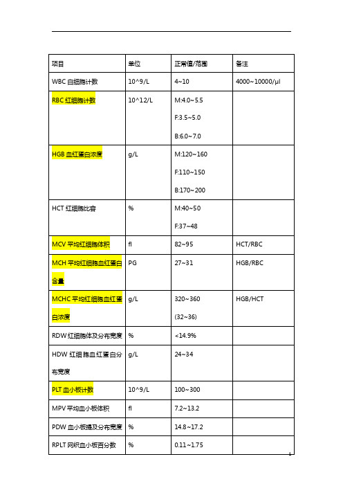
>50:肝纤维化
>130:肝硬化
##################################
###########################################
Ccr 肌酐清除率
ml/min
80~120
CREA 或 Scr 血肌酐
μmol/L
44~133
UA 血尿酸
μmol/L
%
65~140
FPS 游离蛋白 S 含量
%
70~140
TPS 总蛋白 S 含量
%
70~140
APC-SR 活化蛋白 C 敏感
>2.0
度比值
n- APC-SR 标 准化 活 化
>0.84
蛋白 C 敏感度比值
5
Plasminogen 纤 溶 酶 原 %
活性
Plasminogen 纤 溶 酶 原 g/L
固时间比患者 PPP 加正常 血浆
人 PRP 的时间延长≤5s PPP:不含血小板的
血浆
血小板代谢产物的测定
TXB2&DM-TXB2
&11-DH-TXB2 三 种代谢产物。。。略。。。
血小板膜糖蛋白的测定
略。。。
血小板自身抗体的测定
略!
FIB-C:Fibrinogen 纤 维 g/L
2~4
蛋白原定量
0.87~1.12
酶时间比值
TT 凝血酶时间
s
16~18,>3 有意义
备注 外源 内源
3
。。。。。。。。。。。。。。。。出凝血疾病的确诊,so 麻烦。。。我真后悔往上写。。。。。。。。。。。。。。。。。。。。。
vWF 含量或功能测定
TPS5420中文资料

TPS5420
SLVS642A – APRIL 2006 – REVISED AUGUST 2006
2-A, WIDE INPUT RANGE, STEP-DOWN SWIFT™ CONVERTER
FEATURES
• • • • • • • • • • • Wide Input Voltage Range: 5.5 V to 36 V Up to 2-A Continuous (3-A Peak) Output Current High Efficiency up to 95% Enabled by 110-mΩ Integrated MOSFET Switch Wide Output Voltage Range: Adjustable Down to 1.22 V with 1.5% Initial Accuracy Internal Compensation Minimizes External Parts Count Fixed 500-kHz Switching Frequency for Small Filter Size Improved Line Regulation and Transient Response by Input Voltage Feed Forward System Protected by Overcurrent Limiting and Thermal Shutdown –40°C to 125°C Operating Junction Temperature Range Available in Small 8-Pin SOIC Package For SWIFT Documentation, Application Notes and Design Software, See the TI Website at /swift
TPS61040中文资料
V O = 18 V200 µS/divFigure 12. Line Transient ResponseV O = 18 V200 µS/div Figure 13. Load Transient ResponseV O = 18 VFigure 14. Start-Up BehaviorIMPORTANT NOTICETexas Instruments Incorporated and its subsidiaries (TI) reserve the right to make corrections, modifications, enhancements, improvements, and other changes to its products and services at any time and to discontinue any product or service without notice. Customers should obtain the latest relevant information before placing orders and should verify that such information is current and complete. All products are sold subject to TI’s terms and conditions of sale supplied at the time of order acknowledgment.TI warrants performance of its hardware products to the specifications applicable at the time of sale in accordance with TI’s standard warranty. Testing and other quality control techniques are used to the extent TI deems necessary to support this warranty. Except where mandated by government requirements, testing of all parameters of each product is not necessarily performed.TI assumes no liability for applications assistance or customer product design. Customers are responsible for their products and applications using TI components. To minimize the risks associated with customer products and applications, customers should provide adequate design and operating safeguards.TI does not warrant or represent that any license, either express or implied, is granted under any TI patent right, copyright, mask work right, or other TI intellectual property right relating to any combination, machine, or process in which TI products or services are used. Information published by TI regarding third–party products or services does not constitute a license from TI to use such products or services or a warranty or endorsement thereof. Use of such information may require a license from a third party under the patents or other intellectual property of the third party, or a license from TI under the patents or other intellectual property of TI.Reproduction of information in TI data books or data sheets is permissible only if reproduction is without alteration and is accompanied by all associated warranties, conditions, limitations, and notices. Reproduction of this information with alteration is an unfair and deceptive business practice. TI is not responsible or liable for such altered documentation.Resale of TI products or services with statements different from or beyond the parameters stated by TI for that product or service voids all express and any implied warranties for the associated TI product or service and is an unfair and deceptive business practice. TI is not responsible or liable for any such statements.Mailing Address:Texas InstrumentsPost Office Box 655303Dallas, Texas 75265Copyright 2002, Texas Instruments Incorporated。
三显示器4K USB-C Dock(DK30CH2DPPD)商品说明说明书

Triple Monitor 4K USB-C Dock with 5x USB 3.0 PortsProduct ID: DK30CH2DPPDThis TAA compliant 4K USB-C™ dock for Mac and Windows® laptops takes productivity to a whole new level, with support for triple 4K monitors - a first in the market. The USB Type-C dock provides 60W charging power, and 5x USB 3.0 ports to connect your peripheral devices. It’s the perfect accessory for your Dell™ XPS 15, Chromebook Pixel™, or another USB-C enabled PC laptop.The dock also connects to USB 3.0 laptops with a USB-A port (using a USB-C to A cable such as theUSB315AC1M, sold separately).Note: Power Delivery to charge your laptop is not available through USB-A, and only dual display is supported.Enhance ProductivityThe 4K USB-C Dock for Mac and Windows lets you create a three-monitor Ultra HD workstation. Connect:2x 4K DisplayPort (DisplayLink) at 4096 x 2160 resolution / 3840 x 2160 @ 60Hz and1x 4K HDMI (DP Alt Mode) at 4096 x 2160 resolution @ 24Hz / 3840 x 2160 @ 30HzFor high-resolution applications, the universal laptop docking station can also connect to a 5K display (5120 x 2880 resolution) at 60Hz, by connecting the two DisplayPort ports to a single 5K display.Powerful ConnectionsThis triple-monitor docking station lets you connect your peripherals to transform your laptop into a full-sized workstation. With five USB 3.0 ports (1x USB Type-C and 4x USB Type-A incl 1x Fast-Charge port), a Gigabit Ethernet port, headset jack and separate 3.5 mm audio and microphone ports, you have all the connections you need for maximum performance.60W Power DeliveryUsing a single cable, the USB-C docking station with Power Delivery (up to 60W) will power and charge your laptop, and power your peripherals with its 120W power adapter.The DK30CH2DPPD is backed by a 3-year warranty and free lifetime technical support.Certifications, Reports and Compatibility Applications•Ideal for 4K video editing or working with high-resolution graphics•Work on multiple documents simultaneously in office applications •View multiple monitors at a glance, in financial or investment firms •Ideal for surveillance and monitoringFeatures•Dock your USB-C equipped Mac or Windows laptop with triple 4K monitors: 2x DisplayPort (DisplayLink) and 1x HDMI (DP Alt Mode)•Connect your USB devices with 5x USB 3.0 ports - 1x USB-C and 4xUSB-A (including Fast-Charge)•Power and charge your laptop with Power Delivery 2.0 (up to 60W)•Add wired network connectivity with the Gigabit Ethernet RJ45 port •Connect to a laptop’s USB-A port with a USB-C to A cable, sold separately (only dual display is supported and PD is not availablethrough USB-A)Warranty 3 YearsHardware4K Support YesBus Type USB-CChipset ID DisplayLink - DL-6950Genesys Logic - GL3523Texas Instruments - TPS65982Parade Technologies - PS176Displays Supported3Fast-Charge Port(s)YesIndustry Standards USB Power Delivery Specification Rev. 2.0USB Battery Charging Specification Rev. 1.2DisplayPort 1.2IEEE 802.3, IEEE 802.3u, IEEE 802.3abUSB 3.0 - Backward compatible with USB 2.0 and 1.1 Performance Auto MDIX YesCompatible Networks10/100/1000 MbpsFull Duplex Support YesMaximum Data Transfer Rate 5 Gbps (USB 3.0)2 Gbps (Ethernet; Full-Duplex)Maximum Digital Resolutions1x HDMI (DP Alt Mode) - 4096 x 2160p @24Hz / 3840 x2160p @30Hz2x DisplayPort (DisplayLink) - 4096 x 2160p @60Hz / 3840x 2160p @60Hz1x 5K DisplayPort using 2 DP video ports - 5120 x 2880@60HzLower resolutions are also supported. For example, if themax is 3840 x 2160p (4K), it also supports 2560 x 1600pand 2560 x 1440p.Type and Rate USB 3.0 - 5 Gbit/sUASP Support YesConnector(s)Connector Type(s) 2 - DisplayPort (20 pin) Female1 - HDMI (19 pin) Female2 - USB Type-C (24 pin) USB 3.0 (5Gbps) Female1 - USB 3.0 A (Fast-Charge, 9 pin) Female3 - USB Type-A (9 pin) USB 3.0 Female1 - RJ-45 Female1 - 3.5 mm Mini-Jack (4 Position) Female2 - 3.5 mm Mini-Jack (3 Position) Female1 - Security Lock Slot FemaleSoftware OS Compatibility Windows® 7, 8, 8.1, 10macOS 10.11 - 10.12, 10.14 - 10.15Chrome OS™ v55+Special Notes / Requirements Note Not all USB-C ports support the full functionality of the USBType-C standard. Ensure that your host USB-C port supportsUSB Power Delivery 2.0 and DP alt mode.4K resolution is supported on all 3 video ports. A 4K-capableDisplayPort display is required to achieve 4Kx2K resolutionsIf connected to a USB 2.0 host port, or if using a USB 2.0host connection cable, performance may be limited (USB 3.0host cable included)USB 3.0 is also known as USB 3.1 Gen 1; this connectivitystandard offers speeds up to 5Gbps5K resolution is supported by connecting the two DisplayPortvideo ports to a single 5K display. A 5K-capable display isrequired to achieve 5K (5120 x 2880 60Hz) resolutionsThe dock connects to the USB-C port on your laptop. Thedock can also be connected to the USB-A port on laptopsusing a USB-C to A cable, sold separately, but only dualdisplay is supported, and Power Delivery to charge yourlaptop is not available through USB-ASystem and Cable Requirements USB-C enabled computer with an available USB Type-C portPower Center Tip Polarity PositiveInput Current 2 AInput Voltage100 - 240 ACOutput Current 6 AOutput Voltage20V DCPlug Type NPower Delivery60WPower Source AC Adapter Included Environmental Humidity0~95% RHOperating Temperature0°C to 60°C (32°F to 140°F)Storage Temperature-20°C to 60°C (-4°F to 140°F) PhysicalCharacteristicsColor Black & SilverMaterial PlasticProduct Height 1.3 in [3.4 cm]Product Length10.6 in [27 cm]Product Width 3.2 in [82 mm]Weight of Product13.6 oz [385 g]Package Height 2.8 in [71 mm]PackagingInformationPackage Length11.7 in [29.6 cm]Package Width 6.3 in [16.1 cm]Shipping (Package) Weight 3.1 lb [1.4 kg]What's in the Box Included in Package 1 - docking station1 - USB-C cable1 - universal power adapter (NA/JP, ANZ)1 - instruction manual1 - add anti-slip rubber padsProduct appearance and specifications are subject to change without notice.。
EPC-2009

Chipset Power DDR Power
TPS51218
TPS51116 TPS51100 TPS6510x
3V-28V input controller + 3A LDO for DDRI/II/III 4.75V to 5.25V input 3A Termination LDO for DDRI/II/III Triple Output LCD Supply w/Linear Regulator & VCOM Buffer Triple Output LCD Supply With Linear Regulator & Power Good Low Input Voltage Compact LCD Bias IC With VCOM Buffer
Vcore
TPS51610 TPS51611 TPS51120
System Power (Dual Phase)
TPS51125 TPS51220
TPS51124
TPS51117
3.0V- 28V Input 0.76 to 5.5V output Synch Step-Down Controller
– TPS51218 D-CAP™ control
• 3V-28V input range • High efficiency
NB Index
LP Index
Hale Waihona Puke etbook Overview• Graphics Power/additional rail
– TPS51218 D-CAP™ control
LCD Bias
Matrix
8.9” ~10‟ LCD LVDS
Matrix Matrix
- 1、下载文档前请自行甄别文档内容的完整性,平台不提供额外的编辑、内容补充、找答案等附加服务。
- 2、"仅部分预览"的文档,不可在线预览部分如存在完整性等问题,可反馈申请退款(可完整预览的文档不适用该条件!)。
- 3、如文档侵犯您的权益,请联系客服反馈,我们会尽快为您处理(人工客服工作时间:9:00-18:30)。
FEATURES DESCRIPTIONAPPLICATIONSVin Vo1Vo3Power GoodVo2Vo43.3 VTPS65140/45Up to 15 V / 400 mAUp to 30 V / 20 mAUp to −12 V / 20 mA2.7 V to 5.8 VTPS65140TPS65145SLVS497B–SEPTEMBER2003–REVISED MARCH2004 TRIPLE OUTPUT LCD SUPPLY WITH LINEAR REGULATOR AND POWER GOOD• 2.7-V to5.8-V Input Voltage Range The TPS65140/145offers a compact and smallpower supply solution to provide all three voltages • 1.6-MHz Fixed Switching Frequencyrequired by thin film transistor(TFT)LCD displays.•3Independent Adjustable OutputsThe auxiliary linear regulator controller can be used •Main Output up to15V With<1%Typical to generate a 3.3-V logic power rail for systems Output Voltage Accuracy powered by a5-V supply rail only.•Negative Output Voltage Down to-12V/20mA The main output Vo1is a1.6-MHz fixed frequency •Positive Output Voltage up to30V/20mA PWM boost converter providing the source drivevoltage for the LCD display.The device is available in •Auxiliary3.3-V Linear Regulator Controllertwo versions with different internal switch current •Internal Soft Startlimits to allow the use of a smaller external inductor •Internal Power-On Sequencing when lower output power is required.The TPS65140has a typical switch current limit of 2.3A and the •Fault Detection of all OutputsTPS65145has a typical switch current limit of1.37A.•Thermal ShutdownA fully integrated adjustable charge pump •System Power Good doubler/tripler provides the positive LCD gate drivevoltage.An externally adjustable negative charge •Available in TSSOP-24and QFN-24pump provides the negative gate drive voltage.Due PowerPAD™Packagesto the high 1.6-MHz switching frequency of thecharge pumps,inexpensive and small220-nF capaci-tors can be used.•TFT LCD Displays for NotebooksAdditionally,the TPS65140/145has a system power •TFT LCD Displays for Monitorsgood output to indicate when all supply rails are •Portable DVD Playersacceptable.For LCD panels powered by5V,only the •Tablet PCs TPS65140/145has a linear regulator controller using •Car Navigation Systems an external transistor to provide a regulated 3.3Voutput for the digital circuits.For maximum safety,the •Industrial Displaysentire device goes into shutdown as soon as one ofthe outputs is out of regulation.The device can beenabled again by toggling the input or the enable(EN)pin to GND.Please be aware that an important notice concerning availability,standard warranty,and use in critical applications of TexasInstruments semiconductor products and disclaimers thereto appears at the end of this data sheet.PowerPAD is a trademark of Texas Instruments.Good V I L1µF3V O1 VTPS65140TPS65145SLVS497B–SEPTEMBER2003–REVISED MARCH2004These devices have limited built-in ESD protection.The leads should be shorted together or the device placed in conductive foam during storage or handling to prevent electrostatic damage to the MOS gates.TYPICAL APPLICATION CIRCUITORDERING INFORMATION(1)The PWP and RGE packages are available taped and reeled.Add an R suffix to the device type(TPS65100PWPR)to order the devicetaped and reeled.The PWPR package has quantities of2000devices per reel,and the the RGER package has3000devices per reel.Without the suffix,the PWP package only,is shipped in tubes with60devices per tube.ABSOLUTE MAXIMUM RATINGSDISSIPATION RATINGSRECOMMENDED OPERATING CONDITIONSELECTRICAL CHARACTERISTICSTPS65140TPS65145SLVS497B–SEPTEMBER 2003–REVISED MARCH 2004over operating free-air temperature range (unless otherwise noted)(1)(1)Stresses beyond those listed under “absolute maximum ratings”may cause permanent damage to the device.These are stressratings only,and functional operation of the device at these or any other conditions beyond those indicated under “recommended operating conditions”is not implied.Exposure to absolute-maximum-rated conditions for extended periods may affect device reliability.(2)All voltage values are with respect to network ground terminal.(1)Refer to the application information section for further information.V in =3.3V,EN =VIN,Vo1=10V,T A =-40°C to 85°C,typical values are at T A =25°C (unless otherwise noted)TPS65140TPS65145SLVS497B–SEPTEMBER 2003–REVISED MARCH 2004ELECTRICAL CHARACTERISTICS (continued)V in =3.3V,EN =VIN,Vo1=10V,T A =-40°C to 85°C,typical values are at T A =25°C (unless otherwise noted)DEVICE INFORMATIONENENR COMPFB2REFGNDDRVC1−C1+C2−/MODE C2+OUT3FB2REFGNDDRVC1−C1+VIS SPGNPGNSUPC2−/MODEC2+OUT3FB3GNDPGPWP PACKAGETOP VIEW RGE PACKAGETOP VIEW TPS65140 TPS65145SLVS497B–SEPTEMBER2003–REVISED MARCH2004 ELECTRICAL CHARACTERISTICS(continued)V in=3.3V,EN=VIN,Vo1=10V,T A=-40°C to85°C,typical values are at T A=25°C(unless otherwise noted)(1)With V in=supply voltage of the TPS65140,Vo4=output voltage of the regulator,V BE=basis emitter voltage of external transistor.(2)The power good goes high when all3outputs(Vo1,Vo2,Vo3)are above their threshold.The power good goes low as soon as one ofthe outputs is below their threshold.TPS65140TPS65145SLVS497B–SEPTEMBER 2003–REVISED MARCH 2004DEVICE INFORMATION (continued)Terminal FunctionsC1−C1+Vo3C2+C2−ENR BASE FB4REFFB2DRVCOMPFB1VINFB3PGGND GND PGND PGNDSUPENTPS65140TPS65145SLVS497B–SEPTEMBER 2003–REVISED MARCH 2004FUNCTIONAL BLOCK DIAGRAMTYPICAL CHARACTERISTICSTable of GraphsI L − Load Current − mA E f f i c i e n c y − %I L − Load Current − mA E f f i c i e n c y − %707580859095V I − Input Voltage − VE f f i c i e n c y − %TPS65140TPS65145SLVS497B–SEPTEMBER 2003–REVISED MARCH 2004EFFICIENCYEFFICIENCYEFFICIENCYvsvsvsLOAD CURRENTLOAD CURRENTINPUT VOLTAGEFigure 1.Figure 2.Figure 3.V SW 10 V/divV O50 mV/divV I = 3.3 VV O = 10 V/300 mAI L 1 A/div 250 ns/div− N −C h a n n e l M a i n S w i t c h −m ΩT A − Free-Air Temperature − °Cr D S (o n )−40−20020406080100T A − Free-Air Temperature − °CS w i t c h i n g F r e q u e n c y − M H zVo1200 mV/div V I = 3.3 VVo1 = 10 V, C O = 22 µF I O50 mA to 250 mA100 µs/divVo1100 mV/divV I = 3.3 VVo1 = 10 V, C O = 2*22 µFI O50 mA to 250 mA100 µs/divV SW 10 V/divV O50 mV/divV I = 3.3 VV O = 10 V/10 mAI L500 mA/div250 ns/divVo15 V/divV I = 3.3 V V O = 10 V,I O = 300 mA500 µs/divI I 500mA/divVo15 V/div V I = 3.3 V V O = 10 V,500 µs/divVo25 V/divVo310 V/divVo1 − Output Voltage − V− O u t p u t C u r r e n t − AI O TPS65140TPS65145SLVS497B–SEPTEMBER 2003–REVISED MARCH 2004TYPICAL CHARACTERISTICS (continued)SWITCHING FREQUENCYr DS(on)N-CHANNEL MAIN SWITCHvsvsPWM OPERATION CONTINUOUSFREE-AIR TEMPERATUREFREE-AIR TEMPERATUREMODEFigure 4.Figure 5.Figure 6.PWM OPERATION AT LIGHT LOADLOAD TRANSIENT RESPONSELOAD TRANSIENT RESPONSEFigure 7.Figure 8.Figure 9.POWER-UP SEQUENCINGSOFT START Vo1Vo2MAXIMUM LOAD CURRENTFigure 10.Figure 11.Figure 12.0.020.040.060.080.100.120.14Vo1 − Output Voltage − V − O u t p u t C u r r e n t − AI O 00.020.040.060.080.100.12101112131415Vo1 − Output Voltage − V− O u t p u t C u r r e n t − AI O DETAILED DESCRIPTIONMain Boost ConverterPower-Good OutputEnable and Power-On Sequencing (EN,ENR)TPS65140TPS65145SLVS497B–SEPTEMBER 2003–REVISED MARCH 2004TYPICAL CHARACTERISTICS (continued)Vo3MAXIMUM LOAD CURRENTVo3MAXIMUM LOAD CURRENTFigure 13.Figure 14.The TPS65140/45consists of a main boost converter operating with a fixed switching frequency of 1.6MHz to allow for small external components.The boost converter output voltage Vo1is also the input voltage,connected via the pin SUP,for the positive and negative charge pump.The linear regulator controller is independent from this system with its own enable pin.This allows the linear regulator controller to continue to operate while the other supply rails are disabled or in shutdown due to a fault condition on one of their outputs.Refer to the functional block diagram for more information.The main boost converter operates with PWM and a fixed switching frequency of 1.6MHz.The converter uses a unique fast response,voltage mode controller scheme with input voltage feedforward.This achieves excellent line and load regulation (0.2%A load regulation typical)and allows the use of small external components.To add higher flexibility to the selection of external component values,the device uses external loop compensation.Although the boost converter looks like a nonsynchronous boost converter topology operating in discontinuous mode at light load,the TPS65140/45maintains continuous conduction even at light load currents.This is achieved with a novel architecture using an external Schottky diode and an integrated MOSFET in parallel connected between SW and SUP (see the functional block diagram).The integrated MOSFET Q2allows the inductor current to become negative at light load conditions.For this purpose,a small integrated P-channel MOSFET with typically 10Ωr DS(on)is sufficient.When the inductor current is positive,the external Schottky diode with the lower forward voltage conducts the current.This causes the converter to operate with a fixed frequency in continuous conduction mode over the entire load current range.This avoids the ringing on the switch pin as seen with a standard nonsynchronous boost converter and allows a simpler compensation for the boost converter.The TPS65140/45has an open-drain power-good output with a maximum sink capability of 1mA.The power-good output goes high as soon as the main boost converter Vo1and the negative and the positive charge pumps are within regulation.The power-good output goes low as soon as one of the outputs is out of regulation.In this case,the device goes into shutdown at the same time.See the electrical characteristics table for the power-good thresholds.The device has two enable pins.These pins should be terminated and not left floating to prevent faulty operation.Pulling the enable pin (EN)high enables the device and starts the power-on sequencing with the main boost converter Vo1coming up first,then the negative and positive charge pumps.The linear regulator has an independent enable pin (ENR).Pulling this pin low disables the regulator,and pulling this pin high enables this regulator.Positive Charge Pump Negative Charge Pump Linear Regulator Controller Soft StartFault ProtectionThermal ShutdownTPS65140TPS65145 SLVS497B–SEPTEMBER2003–REVISED MARCH2004If the enable pin(EN)is pulled high,the device starts its power-on sequencing.The main boost converter starts up first with its soft start.If the output voltage has reached91.25%of its output voltage,the negative charge pump comes up next.The negative charge pump starts with a soft start and when the output voltage has reached91%of the nominal value,the positive charge pump comes up with the soft start.Pulling the enable pin low shuts down the device.Dependent on load current and output capacitance,each of the outputs comes down.The TPS65140/45has a fully regulated integrated positive charge pump generating Vo3.The input voltage for the charge pump is applied to the SUP pin that is equal to the output of the main boost converter Vo1.The charge pump is capable of supplying a minimum load current of20mA.Higher load currents are possible depending on the voltage difference between Vo1and Vo3.See Figure13and Figure14.The TPS65140/45has a regulated negative charge pump using two external Schottky diodes.The input voltage for the charge pump is applied to the SUP pin that is connected to the output of the main boost converter Vo1. The charge pump inverts the main boost converter output voltage and is capable of supplying a minimum load current of20mA.Higher load currents are possible depending on the voltage difference between Vo1and Vo2. See Figure12.The TPS65140/45includes a linear regulator controller to generate a3.3-V rail which is useful when the system is powered from a5-V supply.The regulator is independent from the other voltage rails of the device and has its own enable(ENR).The main boost converter as well as the charge pumps and linear regulator have an internal soft start.This avoids heavy voltage drops at the input voltage rail or at the output of the main boost converter Vo1during start-up caused by high inrush currents.See Figure10and Figure11.All of the outputs of the TPS65140/45have short-circuit detection and cause the device to go into shutdown.The main boost converter has overvoltage and undervoltage protection.If the output voltage Vo1rises above the overvoltage protection threshold of typically5%of Vo1,then the device stops switching,but remains operational. When the output voltage falls below this threshold,the converter continues operation.When the output voltage falls below the undervoltage protection threshold of typically8.75%of Vo1,because of a short-circuit condition, the TPS65140/45goes into shutdown.Because there is a direct pass from the input to the output through the diode,the short-circuit condition remains.If this condition needs to be avoided,a fuse at the input or an output disconnect using a single transistor and resistor is required.The negative and positive charge pumps have an undervoltage lockout(UVLO)to protect the LCD panel of possible latch-up conditions due to a short-circuit condition or faulty operation.When the negative output voltage is typically above9.5%of its output voltage (closer to ground),then the device enters shutdown.When the positive charge pump output voltage,Vo3,is below8%typical of its output voltage,the device goes into shutdown.See the fault protection thresholds in the electrical characteristics table.The device is enabled by toggling the enable pin(EN)below0.4V or by cycling the input voltage below the UVLO of1.7V.The linear regulator reduces the output current to20mA typical under a short-circuit condition when the output voltage is typically<1V.See the functional block diagram.The linear regulator does not go into shutdown under a short-circuit condition.A thermal shutdown is implemented to prevent damage due to excessive heat and power dissipation.Typically, the thermal shutdown threshold is160°C.If this temperature is reached,the device goes into shutdown.The device can be enabled by toggling the enable pin to low and back to high or by cycling the input voltage to GND and back to V I again.APPLICATION INFORMATIONBOOST CONVERTER DESIGN PROCEDURED +V out V D *Vin V out V D *V sw +10V 0.8V *3.3V 10V 0.8V *0.5V+0.73I L *Iout 1 D *300mA 1 0.73*1.11A p i L+ƪV in *V sw Ť Df s L+(3.3V *0.5V) 0.731.6MHz 4.2m H+304mAI swpeak *I L p iL 2*1.11A 304mA 2*1.26A Inductor SelectionTPS65140TPS65145SLVS497B–SEPTEMBER 2003–REVISED MARCH 2004The first step in the design procedure is to calculate the maximum possible output current of the main boost converter under certain input and output voltage conditions.Below is an example for a 3.3-V to 10-V conversion:V in =3.3V,V out =10V,Switch voltage drop V sw =0.5V,Schottky diode forward voltage V D =0.8V 1.Duty cycle:2.Average inductor current:3.Inductor peak-to-peak ripple current:4.Peak switch current:The integrated switch,the inductor,and the external Schottky diode must be able to handle the peak switch current.The calculated peak switch current has to be equal or lower to the minimum N-MOSFET switch current limit as specified in the electrical characteristics table (1.6A for the TPS65140and 0.96A for the TPS65145).If the peak switch current is higher,then the converter cannot support the required load current.This calculation must be done for the minimum input voltage where the peak switch current is highest.The calculation includes conduction losses like switch r DS(on)(0.5V)and diode forward drop voltage losses (0.8V).Additional switching losses,inductor core and winding losses,etc.,require a slightly higher peak switch current in the actual application.The above calculation still allows for a good design and component selection.Several inductors work with the TPS65140.Especially with the external compensation,the performance can be adjusted to the specific application requirements.The main parameter for the inductor selection is the saturation current of the inductor which should be higher than the peak switch current as calculated above with additional margin to cover for heavy load transients and extreme start-up conditions.Another method is to choose the inductor with a saturation current at least as high as the minimum switch current limit of 1.6A for the TPS65140and 0.96A for the TPS65145.The different switch current limits allow selection of a physically smaller inductor when less output current is required.The second important parameter is the inductor dc ually,the lower the dc resistance,the higher the efficiency.However,the inductor dc resistance is not the only parameter determining the efficiency.Especially for a boost converter where the inductor is the energy storage element,the type and material of the inductor influences the efficiency as well.Especially at high switching frequencies of 1.6MHz,inductor core losses,proximity effects,and skin effects become more ually,an inductor with a larger form factor yields higher efficiency.The efficiency difference between different inductors can vary between 2%to 10%.For the TPS65140,inductor values between 3.3µH and 6.8µH are a good choice but other values can be used as well.Possible inductors are shown in Table 1.Output Capacitor Selectionp V out ƪI outC out Ť1f s +I p LV out *V d +Vin*I p ESRI p = Peak current as described in the previous section peak current controlL = Selected inductor value I out = Nominal load current f s = Switching frequencyV d = Rectifier diode forward voltage (typically 0.3 V)C out = Selected output capacitor ESR = Output capacitor ESR valueInput Capacitor SelectionRectifier Diode SelectionTPS65140TPS65145SLVS497B–SEPTEMBER 2003–REVISED MARCH 2004APPLICATION INFORMATION (continued)Table 1.Inductor SelectionFor best output voltage filtering,a low ESR output capacitor is recommended.Ceramic capacitors have a low ESR value but depending on the application,tantalum capacitors can be used as well.A 22-µF ceramic output capacitor works for most of the applications.Higher capacitor values can be used to improve load transient regulation.See Table 2for the selection of the output capacitor.The output voltage ripple can be calculated as:with:For good input voltage filtering,low ESR ceramic capacitors are recommended.A 22-µF ceramic input capacitor is sufficient for most of applications.For better input voltage filtering,this value can be increased.See Table 2and the typical applications for input capacitor recommendations.Table 2.Input and Output Capacitors SelectionTo achieve high efficiency,a Schottky diode should be used.The voltage rating should be higher than the maximum output voltage of the converter.The average forward current should be equal to the average inductor current of the converter.The main parameter influencing the efficiency of the converter is the forward voltage and the reverse leakage current of the diode;both should be as low as possible.Possible diodes are:On Semiconductor MBRM120L,Microsemi UPS120E,and Fairchild Semiconductor MBRS130L.Converter Loop Design and StabilityDesign Procedure Quick StepsSetting the Output Voltage and Selecting the Feedforward Capacitor V out +1.146V ƪ1*R1R2ŤFV O 1Up to 10 V/150 mAC8*12 p f z R1*12 p 50kHz R1TPS65140TPS65145SLVS497B–SEPTEMBER 2003–REVISED MARCH 2004The TPS65140/45converter loop can be externally compensated and allows access to the internal transconductance error amplifier output at the COMP pin.A small feedforward capacitor across the upper feedback resistor divider speeds up the circuit as well.To test the converter stability and load transient performance of the converter,a load step from 50mA to 250mA is applied and the output voltage of the converter is monitored.Applying load steps to the converter output is a good tool to judge the stability of such a boost converter.1.Select the feedback resistor divider to set the output voltage.2.Select the feedforward capacitor to place a zero at 50kHz.3.Select the compensation capacitor on pin COMP.The smaller the value,the higher the low frequency gain.e a 50-k Ωpotentiometer in series to C c and monitor V out during load transients.Fine tune the load transient by adjusting the potentiometer.Select a resistor value that comes closest to the potentiometer resistor value.This needs to be done at the highest V in and highest load current because stability is most critical at these conditions.The output voltage is set by the external resistor divider and is calculated as:Across the upper resistor,a bypass capacitor is required to speed up the circuit during load transients as shown in Figure 15.Figure 15.Feedforward CapacitorTogether with R1the bypass capacitor C8sets a zero in the control loop at approximately 50kHz:A value closest to the calculated value should be rger feedforward capacitor values reduce the load regulation of the converter and cause load steps as shown in Figure 16.Load Step Compensationf z*12p Cc RcC C = 4.7 nFTPS65140TPS65145 SLVS497B–SEPTEMBER2003–REVISED MARCH2004Figure16.Load Step Caused By A Too Large Feedforward Capacitor ValueThe regulator loop can be compensated by adjusting the external components connected to the COMP pin.The COMP pin is connected to the output of the internal transconductance error amplifier.A typical compensation scheme is shown in Figure17.pensation NetworkThe compensation capacitor C c adjusts the low frequency gain,and the resistor value adjusts the high frequency gain.The following formula calculates at what frequency the resistor increases the high frequency gain.Lower input voltages require a higher gain and a lower compensation capacitor value.A good start is C c=1nF for a3.3-V input and C c=2.2nF for a5-V input.If the device operates over the entire input voltage range from 2.7V to5.8V,a larger compensation capacitor up to10nF is recommended.Figure18shows the load transient with a larger compensation capacitor,and Figure19shows a smaller compensation capacitor.Figure18.C C=4.7nFC C= 1 nFTPS65140TPS65145SLVS497B–SEPTEMBER 2003–REVISED MARCH 2004Figure 19.C C =1nFLastly,R c needs to be selected.A good practice is to use a 50-k Ωpotentiometer and adjust the potentiometer for the best load transient where no oscillations should occur.These tests have to be done at the highest V in and highest load current because the converter stability is most critical under these conditions.Figure 20,Figure 21,and Figure 22show the fine tuning of the loop with R c .Figure 20.Overcompensated (Damped Oscillation),R C Is Too LargeFigure 21.Undercompensated (Loop Is Too Slow),R C Is Too SmallV out ƪ+VREF Ť1*R3R4 *V REF ƪ+1.213V Ť1*R3R4*1.213V R3ƪR4 ȧȱȲŤV out Ť*V REF V REF +1ȧȳȴƪR4 ŤV out Ť*1.2131.213+1TPS65140TPS65145SLVS497B–SEPTEMBER 2003–REVISED MARCH 2004Figure 22.Optimum,R C Is IdealNegative Charge PumpThe negative charge pump provides a regulated output voltage by inverting the main output voltage,Vo1.The negative charge pump output voltage is set with external feedback resistors.The maximum load current of the negative charge pump depends on the voltage drop across the external Schottky diodes,the internal on resistance of the charge pump MOSFETS Q8and Q9,and the impedance of the flying capacitor,C12.When the voltage drop across these components is larger than the voltage difference from Vo1to Vo2,the charge pump is in drop out,providing the maximum possible output current.Therefore,the higher the voltage difference between Vo1and Vo2,the higher the possible load current.See Figure 12for the possible output current versus boost converter voltage Vo1and the calculations below.Vout min =-(Vo1-2V D -Io (2×r DS(on)Q8+2×r DS(on)Q9+X cfly ))Setting the output voltage:The lower feedback resistor value,R4,should be in a range between 40k Ωto 120k Ωor the overall feedbackresistance should be within 500k Ωto 1M Ω.Smaller values load the reference too heavy and larger values may cause stability problems.The negative charge pump requires two external Schottky diodes.The peak current rating of the Schottky diode has to be twice the load current of the output.For a 20mA output current,the dual Schottky diode BAT54or similar is a good choice.Positive Charge PumpThe positive charge pump can be operated in a voltage doubler mode or a voltage tripler mode depending on the configuration of the C2+and C2-/MODE pins.Leaving the C2+pin open and connecting C2-/MODE to GND forces the positive charge pump to operate in a voltage doubler mode.If higher output voltages are required the positive charge pump can be operated as a voltage tripler.To operate the charge pump in the voltage tripler mode,a flying capacitor needs to be connected to C2+and C2-/MODE.The maximum load current of the positive charge pump depends on the voltage drop across the internal Schottky diodes,the internal on-resistance of the charge pump MOSFETS,and the impedance of the flying capacitor.When the voltage drop across these components is larger than the voltage difference Vo1×2to Vo3(doubler mode)or Vo1×3to Vo3(tripler mode),then the charge pump is in dropout,providing the maximum possible output current.Therefore,the higher the voltage difference between Vo1×2(doubler)or Vo1×3(tripler)to Vo3,the higher the possible load current.See Figure 13and Figure 14for output current versus boost converter voltage,Vo1,and the following calculations.Voltage doubler:Vo3max =2×Vo1-(2V D +2×Io ×(2×r DS(on)Q5+r DS(on)Q3+r DS(on)Q4+X C1))V out +1.214 ƪ1*R5R6ŤR5+R6ƪV out V FB*1Ť+R6ƪV out 1.214*1ŤTPS65140TPS65145SLVS497B–SEPTEMBER 2003–REVISED MARCH 2004Voltage tripler:Vo3max =3×Vo1-(3×V D +2×Io ×(3×r DS(on)Q5+r DS(on)Q3+r DS(on)Q4+X C1+X C2))The output voltage is set by the external resistor divider and is calculated as:Linear Regulator ControllerThe TPS65100/05includes a linear regulator controller to generate a 3.3-V rail when the system is powered from a 5-V supply.Because an external npn transistor is required,the input voltage of the TPS65140/45applied to VIN needs to be higher than the output voltage of the regulator.To provide a minimum base drive current of 13.5mA,a minimum internal voltage drop of 500mV from V in to V base is required.This can be translated into a minimum input voltage on VIN for a certain output voltage as the following calculation shows:Vin min =Vo4+V BE +0.5VThe base drive current together with the h FE of the external transistor determines the possible output ing a standard npn transistor like the BCP68allows an output current of 1A and using the BCP54allows a load current of 337mA for an input voltage of 5V.Other transistors can be used as well,depending on the required output current,power dissipation,and PCB space.The device is stable with a 4.7-µF ceramic output rger output capacitor values can be used to improve the load transient response when higher load currents are required.Thermal InformationAn influential component of the thermal performance of a package is board design.To take full advantage of the heat dissipation abilities of the PowerPAD or QFN package with exposed thermal die,a board that acts similar to a heatsink and allows for the use of an exposed (and solderable)deep downset pad should be used.For further information.see Texas Instrumens application notes (SLMA002)PowerPAD Thermally Enhanced Package ,and (SLMA004)Power Pad Made Easy .For the QFN package,see the application report (SLUA271)QFN/SON PCB Attachement .Layout ConsiderationsFor all switching power supplies,the layout is an important step in the design,especially at high-peak currents and switching frequencies.If the layout is not carefully designed,the regulator might show stability and EMI problems.Therefore,the traces carrying high-switching currents should be routed first using wide and short traces.The input filter capacitor should be placed as close as possible to the input pin VIN of the IC.See the evaluation module (EVM)for a layout example.。