Temperature-dependent electroluminescence from InGaN_GaN green light-emitting diodes on silicon
在电场作用下迁移产生导电现象。本...
摘要L聚合物电致发光材料是近几年来取得突破性进展而倍受关注的新兴功能材料。
它们的电致发光薄膜器件激发电压低、发光效率高、易得到彩色显示,而且容易实现大屏幕平板化。
研究发现聚对苯乙炔类聚合物具有许多优异的性能,如柔性好、驱动电压低、能带结构可调、优良的溶解性及耐热性等。
人们已经制备出发红光、黄光、绿光的性能优异的聚对苯乙炔类聚合物制成的电致发光器件;而能发蓝色光的该类聚合物材料则很少,性能也差,限制了该类材料在全色显示方面的应用。
『『本文制备出一种新型的、能发蓝色光的聚对苯乙炔类聚合物材料聚【(2,5.二亚甲基.1,3,4.嗯二唑)二氧代.1,4.亚苯基.1,2一亚乙烯基.1,4.亚苯基.1,2.亚乙烯基.1,4一亚苯基】,并对其进行了溶解性、电性能、光性能、热性能的研究。
实验结果说明它的荧光发射最大波长为472nm,属于蓝色发光范围。
电导率的测定结果说明它比传统的PPV类电致发光材料有更强的电子与空穴的复合几率。
它的能带宽度(Eg)为3.84eV。
荧光量子效率巾=o.995。
(该聚合物能溶解于氯仿及四氢呋喃等有机溶剂中。
其分解温度大于350‘C。
TGA的分析结果说明该聚合物具有优异的热稳定性。
上关键词:电致发光,聚对苯乙炔衍生物,蓝色光ABSTRACTInrecentyears,electroluminescenceofpolymerhasbeenmadewithanoutstandingprogress,andcloseattentionispaidonthesekindsofnewfunctionmaterials.Theadvantagesareasfollows:lowexcitingvoltage,highefficiencyofelectroluminescentcellsinthinfilms,easinessofcolorlightemission,andattractivematerialsforlarge·areavisiblelight-emittingdiodes.Poly(p·phenyleneVinylene)(PPV)isthefirstpolymermaterialfoundtohavetheelctroluminesencepropertiesandwasintensivelystudied.PPVderivativeshavedemonstratedvariouscolorswithimpressiveefficiency,brightness,flexibilityanduniformity.ThePPVderivatives,whichemitredlight,yellowlightandgreenlight,canbeeasilyobserved,exceptforbluelight.Forseveralreasons,apolymeremittingbluelightisparticularlydesirable.InthispapeLpoly[(2,5-dimethylene.I,3,4.oxadiazole)dioxy‘1,4。
温度对短链多烯生物分子β胡萝卜素拉曼光谱的影响

了研究 , 发现在不同溶剂中, 同溶液浓度下其拉曼散射强度( 不 散射截面) ] 不同 .其机理为 : 同环 不
境下 胡 萝 卜 素分 子结 构有 序性程 度不 同 ,其产 生 的相 干弱 阻尼 C C键 振 动强 度 不 同 , 拉 曼散 射截 — 其
面不 同 j .键状 多烯 分子 结构 有序 程度不 仅对 拉曼散 射截 面有很 大 影 响 ,对谱 线 宽度 及 频率 也有 着 重 要 影响 .很 多生 物过程 和化 学反应 在 液体 中进行 , 体 中生 物分 子结 构 与 性 能研 究 更有 实 际 意义 .多 液 烯 类线性 生 物分子 结构 有序 性 与 温度 密 切 相 关 ,在 一定 温 度 下 ,多 烯 类 线 性链 状 分 子结 构 有 序 程 度 高 ,『电子离域 扩展 , 分子 具有 特殊光 学性质 ,如拉 曼散射 截 面增大 , 阶非 线性 系数提 高. 7 使 三
王微微 , 亮。 李 占龙 孙成林 , 阳顺利 许 大鹏 李 , , 一 欧 , ,
曲冠男 ,里佐威 一,高淑琴 ,曹军胜。 郜峰 利 , ,周 强
( .吉林 大学超 硬材料 国家重点实验室 ,长春 102 ; .吉林大学物理学院 , I 301 2 长春 10 2 ; 3 0 3
联 系 人 简 介分 子 光谱 研 究 .Ema : h nl @j .d .n 孙 博 ・ i c egn l eu c l i u
N . o9
王 微 微 等 :温 度 对 短 链 多烯 生物 分子 / 萝 卜素拉 曼 光 谱 的 影 响 3胡
本 文研究 了温 度对 胡 萝 卜 素共振 拉曼光 谱 的影 响 , 究结 果对认 识 多烯类 线性 链 状分 子 的性 质 研
LCD英语缩写词汇
目前最全的液晶专业术语Backlight:背光。
CCFL(CCFT) (Cold Cathode Fluorescent Light/Tube):冷阴极荧光灯。
Composite vide复合视频。
Component vide分量视频。
COB(Chip On Board):IC裸片通过邦定固定于印刷线路板上。
COF(Chip On Film):将IC封装于柔性线路板上。
COG(Chip On Glass):将IC封装于玻璃上。
CRT(Cathode Radial Tube):阴极射线管。
DPI(Dot Per Inch):点每英寸。
Duty:占空比,高出点亮的阀值电压的部分在一个周期中所占的比率。
DVI(Digital Visual Interface):(VGA)数字接口。
ECB(Electrically Controlled Birefringence):电控双折射。
EL(Electro luminescence):电致发光。
EL层由高分子量薄片构成FSTN(Formulated STN):薄膜补偿型STN,用于黑白显示。
HTN(High Twisted Nematic):高扭曲向列的显示类型。
IC(Integrate Circuit):集成电路。
Inverter:逆变器。
ITO(Indium-Tin Oxide):氧化铟锡。
LCD(Liquid Crystal Display):液晶显示器。
LCM(Liquid Crystal Module): 液晶模块。
LED(Light Emitting Diode):发光二极管。
LVDS(Low Voltage Differential Signaling):低压差分信号。
NTSC(National Television Systems Committee):NTSC制式,全国电OSD(On Screen Display):在屏上显示。
PAL(Phase Alternating Line)AL制式(逐行倒相制式)。
纳米管制作皮肤感应器 翻译 中英
最后译文:纳米管弹性制作出皮肤般的感应器美国斯坦福大学的研究者发现了一种富有弹性且透明的导电性能非常好的薄膜,这种薄膜由极易感触的碳纳米管组成,可被作为电极材料用在轻微触压和拉伸方面的传感器上。
“这种装置也许有一天可以被用在被截肢者、受伤的士兵、烧伤方面接触和压迫的敏感性的恢复上,也可以被应用于机器人和触屏电脑方面”,这个小组如是说。
鲍哲南和他的同事们在他们的弹透薄膜的顶部和底部喷上一种碳纳米管的溶液形成平坦的硅板,覆盖之后,研究人员拉伸这个胶片,当胶片被放松后,纳米管很自然地形成波浪般的结构,这种结构作为电极可以精准的检测出作用在这个材料上的力量总数。
事实上,这种装配行为上很像一个电容器,用硅树脂层来存储电荷,像一个电池一样,当压力被作用到这个感应器上的时候,硅树脂层就收紧,并且不会改变它所储存的电荷总量。
这个电荷是被位于顶部和底部的硅树脂上的纳米碳管测量到的。
当这个复合膜被再次拉伸的时候,纳米管会自动理顺被拉伸的方向。
薄膜的导电性不会改变只要材料没有超出最初的拉伸量。
事实上,这种薄膜可以被拉伸到它原始长度的2.5倍,并且无论哪种方向不会使它受到损害的拉伸它都会重新回到原始的尺寸,甚至在多次被拉伸之后。
当被充分的拉伸后,它的导电性喂2200S/cm,能检测50KPA的压力,类似于一个“坚定的手指捏”的力度,研究者说。
“我们所制作的这个纳米管很可能是首次可被拉伸的,透明的,肤质般感应的,有或者没有碳的纳米管”小组成员之一Darren Lipomi.说。
这种薄膜也可在很多领域得到应用,包括移动设备的屏幕可以感应到一定范围的压力而不仅限于触摸;可拉伸和折叠的几乎不会毁坏的触屏感应器;太阳能电池的透明电极;可包裹而不会起皱的车辆或建筑物的曲面;机器人感应装置和人工智能系统。
其他应用程序“其他系统也可以从中受益—例如那种需要生物反馈的—举个例子,智能方向盘可以感应到,如果司机睡着了,”Lipomi补充说。
通常的化合物结晶是通过降温实现,但这篇钙钛矿的结晶是通过升温实现的,而且速度超快,还是单晶-2015-NC
of Physical Sciences and Engineering, Solar and Photovoltaics Engineering Research Center, King Abdullah University of Science and Technology (KAUST), Thuwal 23955-6900, Kingdom of Saudi Arabia. 2 Department of Chemistry, Faculty of Science, Mansoura University, Mansoura 35516, Egypt. 3 Mathematical Institute, University of Oxford, Woodstock Road, Oxford OX2 6GG, UK. 4 Materials Science and Engineering, King Abdullah University of Science and Technology (KAUST), Thuwal 23955-6900, Kingdom of Saudi Arabia. 5 Imaging and Characterization Lab, King Abdullah University of Science and Technology (KAUST), Thuwal 23955-6900, Kingdom of Saudi Arabia. * These authors contributed equally to this work. Correspondence and requests for materials should be addressed to O.M.B. (email: osman.bakr@.sa).
PbS胶质量子点太阳能电池的性能参数及主要结构
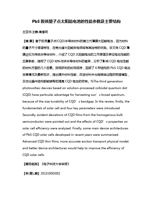
PbS胶质量子点太阳能电池的性能参数及主要结构王亚非;王静;高椿明【摘要】基于胶质量子点(CQD)半导体材料的第三代薄膜太阳能电池,因为材料的量子尺寸调谐特性,在宽光谱太阳能发电领域有其独特的优势。
该文将CQD薄膜近似为传统半导体材料,介绍了CQD太阳能电池的工作原理及表征电池性能的主要参数,指明了CQD材料与块半导体材料的差异,分析了影响CQD电池性能的材料方面的几个因素。
按照研究的时间顺序,回顾了6种结构的PbS CQD电池发展情况及最新现状,指出提升材料性能,改进材料中光电转换过程的物理模型,及优化器件结构都能够帮助提高CQD电池的效率。
%The third generation photovoltaic devices based on solution-processed colloidal quantum dot (CQD) have particular advantage for harvesting sun’s broad spectrum, because of the size tunability of CQD’s bandgap. In the review, firstly, the fundamentals of solar cell and four key parameters were introduced. Secondly, evident deviations of CQD films from the homogenous bulk semiconductor were pointed out and the effects of CQD’s properties on solar cell efficiency were analyzed. Finally, some main device architectures of PbS CQD solar cells developed in recent years were summarized. Advanced CQD thin films, more accurate exciton transport physical model, and better device architectures would help to improve the efficiency of CQD solar cells.【期刊名称】《电子科技大学学报》【年(卷),期】2015(000)002【总页数】7页(P299-305)【关键词】载流子输运;胶质量子点;P-N结;太阳能电池【作者】王亚非;王静;高椿明【作者单位】电子科技大学光电信息学院成都 610054;电子科技大学光电信息学院成都 610054;电子科技大学光电信息学院成都 610054【正文语种】中文【中图分类】TN2日趋严峻的能源紧缺、环境污染等问题,促使人们必须发展一种能够同时满足高效和低成本要求的光伏发电技术。
【精品】薄膜电池英文述语
薄膜电池材料及术语(中英文对照) AAcetone-丙酮Adjustment-调整,调节Aluminium(Al)-铝Arqon(Ar)-氩气Alternatingcurrent(AC)-交流电Ammonia(NH3)-氨气Amorphous-非晶的Anneal-退火Assembly-组装averagepower-平均功率BBackplane背板Backconductor-背电极Backelectrode-背电极balancegas-平衡气B2H6-硼烷Bouding-绑定Buffer-缓冲器built-involtage-内建电压BuildingIntegratedPhotovoltaic-建筑一体化CCable-电缆Carrier-运送者,搬运器Coverglass-覆盖玻璃ChemicalVaporDeposition(CVD)-化学气相沉积Commit-提交,答应负责Copper(Cu)-铜Contamination-污染,玷污Conversion-转换,转化Cumulate-adj.累积的;v.累积Cathode-阴极Crystalline-晶体的Crystallite-微晶Chamber-室,房间Curve-曲线DDenser-密集的,浓厚的Deviation-背离,偏离Diffusion-扩散,传播,漫射Diode-二极管Doublesidestickingtape-双边粘结带Deposition-沉积Drill-钻孔Dielectric-电介质,绝缘体Directcurrent(DC)-直流电Dilution-稀释driftcurrent-漂移电流EEdge-边缘,边EVA-乙烯-醋酸乙烯共聚物Evaporation-蒸发,蒸镀Etch-蚀刻efficiency-效率Encapsulation-封装Energy-能量FFastglue-快干胶Feature-特征,特色Flux-流量Foil-金属薄片Flaming-烧结Fabrication-制作,构成Furnace-熔炉,炉子GGlasswashingdetergent-玻璃清洗液Guarantee-保证,担保HHydrogen(H2)-氢气Helium(He)-氦气Ii-layer-i-层,本征层Infra-red(IR)-红外线I-V-电流-电压IncidenceWaves-入射波initial-初始的,最初的Installation-安装,装置JJunction-结KLLaser-Scribing-镭射分层,激光划线Layout-平面图Lamination-层压,迭片Laminators层压机Lift-升距Liquidnitroqen-液氮MMagnetron-磁电管Maintenance-维修,维护Maskingtape-包装带Maskingpaper-包装纸Methane(CH4)-甲烷Micromorph-微晶Module-模组Modify-更改,修改MetalorganicChemicalVaporDeposition(MOCVD)-金属有机化学气相沉积NNitrogen(N2)-氮气NF3-三氟化氮n-layer-n-层,含电子较多,掺N或POon-grid-并网organization-组织,机构,团体Oven-烤箱,烤炉Output-产量Outdoor-户外的PPattern-V.形成,图案化;n.模式,图案PBS-聚(丁二烯-苯乙烯)PBT-聚对苯二甲酸丁二酯peakwatt-峰瓦Plasma-等离子PlasmaEnhanceChemicalVaporDeposition(PECVD)-等离子增强化学气相沉积p-layer-p层,空穴较多,掺硼Pilot-试生产Phosipine(PH3)-膦烷Power-功率pottedcomponent-密封元件Preheat预热Preliminary-初步的Pressure-压力PVB-聚乙烯醇缩丁醛树脂PhysicalVaporDeposition(PVD)—物理气相沉积PESC电池-发射结钝化太阳电池QQualityassessment(QA)-质量评价Qualitycontrol(QC)-质量控制,质量管理Qualification-资格,资质RRadiofrequency(RF)-射频Recombination-复合Rise-升程Reliability-可靠性SSandblastingmaterial-喷沙材料Seal-密封Sealbelt-密封带Sealgum-密封胶Sealingarrangement-密封装置Semiconductor-半导体Silane(SiH4)-硅烷Siliconrubber-硅胶Silver(Ag)-银Singlejunction-单结Solar-太阳的,太阳能的Solarcell-太阳能电池Solarsimulator-太阳光模拟器Solder-焊料,焊接Sputter-溅射Sodiumbisulfide-硫化钠Sodiumcloride-氯化钠SF6-六氟化硫Substrate-底物,基板Specify-指定,详细说明TTandem-叠层Target-靶材Tedlar-聚乙烯氟化物薄膜TemperatureCoefficient-温度系数Thinfilm-薄膜TPT-太阳能背膜TPE-磷酸三苯酯,薄膜电池封装材料之一TransparentConductiveOxide(TCO)-透明导电氧化层Trap-诱捕Trimethylborate<B(CH3)3>-三甲基硼Trimmer-整理,清理Texturing-织构turn-keysolution-交钥匙工程UUV-紫外Ultravacuum-超中空Vgloves-手套Vacuum-真空,空间VeryHighFreqency(VHF)-甚高频Vertical-垂直的WWafer-晶片,圆片,硅片Wiring-配线ZZinc(Zn)-锌常用符号Js-反向饱和电流密度R-反射系数T-透射系数α-吸收系数λ-波长Voc-开路电压:在p-n开路情况下(R=∞),p-n结两端的电压。
Temperature dependence of density profiles for a cloud of non-interacting fermions moving i

I. INTRODUCTION
The achievement of Bose-Einstein condensation in ultracold gases of bosonic atoms has given great impulse to the study of dilute quantum gases inside magnetic or optical traps [1]. Similar cooling and trapping techniques are being used to drive gases of fermionic alkali atoms into the quantum degeneracy regime [2]. It is also possible to experimentally generate and study strongly anisotropic atomic fluids effectively approaching dimensionality D = 2 or D = 1, at very low temperature and with very high purity, inside magnetic traps where the transverse and the longitudinal confinement are vastly different [3]. In the relevant conditions of temperature and dilution the atomic interactions become negligible in a gas of fermions placed in a single Zeeman sublevel inside a magnetic trap [4]. One can obtain in this way a close laboratory realization of an inhomogeneous, non-interacting Fermi gas, which has special significance in regard to the foundations of density functional theory and to tests of the Thomas-Fermi approximation [5]. In the quasi-onedimensional (1D) case the ground state and the excitation spectrum of such an ideal gas of spin-polarized (or ”spinless”) fermions can be mapped into those of a gas of hard-core impenetrable bosons [6]. The latter is known as the Tonks gas, from the early work of Tonks [7] on the equation of state of hard-object adsorbates. Advances in atom waveguide technology, with potential applications to atom interferometry and integrated atom optics, especially motivate theoretical studies of dilute gases in a regime where the dynamics becomes essentially 1D [8]. The wave functions of a cloud of spinless fermions under harmonic confinement are, of course, Slater determinants of harmonic-oscillator single-particle orbitals. Their representation in terms of Hermite polynomials has, however, limited usefulness for numerical calculations on mesoscopic clouds [9]. Brack and van Zyl [10] have developed a more powerful method for non-interacting fermions occupying a set of closed shells under isotropic harmonic confinement in D dimensions, leading to analytical expressions for the particle and kinetic energy densities at temperature T = 0 in terms of Laguerre polynomials. These expressions are especially useful for numerical calculations on isotropic systems in D = 2 and D = 3. A Green’s function method, which altogether avoids the use of wave functions in favor of the matrix elements of the position and momentum operators, has been developed for similar purposes [11] and extended to calculations of the pair distribution function in the ground state for the 1D ideal Fermi gas [12]. This method has also been extended to the ground state of ideal Fermi gases under harmonic confinement of arbitrary anisotropy in higher dimensionalities [13]. The purpose of the present paper is to extend the Green’s function method to an inhomogeneous 1D cloud of noninteracting fermions at finite temperature and to illustrate its usefulness by numerical calculations of the particle and kinetic energy density profiles as functions of temperature in the case of harmonic confinement. Analytical expressions have been derived by Wang [14] for the same system at high temperature, where the chemical potential is lower than the single-particle ground-state energy. The case of non-interacting fermions under 3D harmonic confinement has been treated by Schneider and Wallis [15] through the use of Laguerre polynomials. The emphasis of our numerical calculations will be to illustrate how the characteristic quantum features of the fermion cloud, i.e. its shell structure and the spill-out of particles at the boundaries beyond the Thomas-Fermi radius, evolve with increasing temperature as a semiclassical regime is being approached.
- 1、下载文档前请自行甄别文档内容的完整性,平台不提供额外的编辑、内容补充、找答案等附加服务。
- 2、"仅部分预览"的文档,不可在线预览部分如存在完整性等问题,可反馈申请退款(可完整预览的文档不适用该条件!)。
- 3、如文档侵犯您的权益,请联系客服反馈,我们会尽快为您处理(人工客服工作时间:9:00-18:30)。
Temperature-dependent electroluminescence from InGaN/GaN green light-emitting diodes on silicon with different quantum-well structuresGuangxu Wang,Xixia Tao,Junlin Liu and Fengyi JiangNational Engineering Technology Research Center for LED on Si Substrate,Nanchang University,Nanchang330047,People’s Republic of ChinaE-mail:guangxuwang@Received10July2014,revised8November2014Accepted for publication11November2014Published15December2014AbstractTemperature-dependent electroluminescence from InGaN/GaN light-emitting diodes(LEDs)grown on Si(111)are investigated.With the increase of current density,internal quantumefficiencies(IQEs)firstly rise accompanied by full width at half maximum(FWHM)shrinkageand then IQEs droop combined with FWHM broadening are presented.With the decline oftemperature,both the maximum of IQEs accompanying the minimum of FWHM shift towardsthe direction of low current density.Moreover,the maximum of IQEs shift faster than theminimum of FWHM for single quantum well LED.Furthermore,it was found that the quantumwell close to n-GaN has priority to radiate in small current injection,especially at lowtemperature(100K)for multiple quantum wells LED.Keywords:electroluminescence,IQEs,FWHM,quantum wells,light-emitting diodes(Somefigures may appear in colour only in the online journal)1.IntroductionThe Nobel Prize in Physics2014was awarded for the invention of efficient blue light-emitting diodes,which has enabled bright and energy-saving white light sources.At the current stage of development,light-emitting diodes(LEDs) are discussed as an energy saving replacement for incandes-cent light bulbs,while their price needs to be reduced and light quality needs to be improved for LEDs to be introduced into the general illumination market.InGaN-based LEDs grown on Si substrates are certainly an excellent candidate for their low-cost materials,large substrate diameters and easy-to-operate manufacture process etc.However,there are also lots of challenges to get high efficient InGaN-based LEDs structures on Si for the large lattice constant mismatch and thermal coefficient mismatch between GaN and Si[1].In the past decade,great efforts have been made to grow InGaN-based blue and green LEDs on Si substrates[2].Light outputs in the magnitude of microwatt to milliwatt for LED on Si using different techniques have also been reported[3,4].In 2009,thefirst blue power LED on Si for commercial use was reported with output power of457mW at a driving current of 350mA emitting in453nm for LED die of1mm2after encapsulation[2,5].Zhu et al,fabricated blue and green LED structures on Si(111)substrates,and observed the light out-puts decreased dramatically as the emission wavelength increased from455nm to510nm[6].High efficient green LED on Si has not been reported yet,and the factors that affect the luminescence efficiency of LEDs on Si substrate have not been investigated clearly.The green quantum wells(QWs)have higher In-com-ponents with more serious piezoelectric polarization effect compared with blue QWs,which increases the band tilt of QWs.That affects carrier distribution,and determines the luminous efficiency of QWs[7].In addition,it was found that several peaks appeared in the emission spectrum of multiple quantum wells(MQWs)and varied with the change of current density[8,9],from which it was considered thatmultiple Semicond.Sci.Technol.30(2015)015018(6pp)doi:10.1088/0268-1242/30/1/015018peaks were emitted from different QWs.Therefore,identify-ing which well the light comes from is very important for improving the luminous efficiency of MQW LED.In this paper,we investigate the temperature-dependent electro-luminescence properties of single quantum well(SQW)and MQW green LEDs grown on Si substrate;dependences of internal quantum efficiencies(IQEs)and full width at half maximum(FWHM)on the injection current density are pre-sented.And we have experimentally confirmed that the quantum well close to n-GaN has priority to radiate in small current injection at low temperature(100K).Such experi-mental phenomena will play a guiding role in understanding the luminous mechanisms of LEDs.2.ExperimentsInGaN/GaN SQW and MQW LED,structures are grown on 0.2mm×0.2mm trenched Si(111)substrates in a7×2inch close-coupled showerhead MOCVD reactor.The epitaxial structure consists of a0.06μm thick AlN nucleation layer grown at900°C,and a0.5μm-thick GaN buffer layer grown at1100°C,followed by an0.05μm thick AlN/AlGaN inter-mediate layer grown at930°C,and a2.8μm thick Si-dopedGaN layer grown at1150°C,then an0.08μm-thick InGaN prepare-layer grown at1100°C,subsequently grown InGaN/ GaN QW region,and a0.015μm thick p-type AlGaN(20% Al)electron blocking layer(EBL)and a0.12μm thick p-type GaN layer grown at1000°C for the LED.Other details of the growth process can be found elsewhere[1,10–12].Three samples with different QWs structures have been grown: Sample I includes three cycles of InGaN/GaN(2nm/14nm) MQW,and subsequently grown an InGaN/GaN(2.2nm/ 5nm)structure,where the growth temperature of InGaN is 770°C.Sample II is the same as sample I,except that thefirst period of InGaN is grown at temperature of775°C.Sample III only includes one cycle of InGaN/GaN(2.2nm/5nm) structure,where the InGaN growth temperature is760°C. Schematicfigures of quantum-well structures of three samples are shown infigures1(b)–(d),Samples I,II and III are named MQW-LED,VWT(varied well-temperature)-LED and SQW-LED,respectively.For three samples,SQW-LED and MQW-LED can form a nice contrast in luminous efficiency and luminescence spectra.It is well known[9]that holes are injected and distributed predominantly in the QW close to the p-GaN layer when the LED is in working condition.There-fore,we designed the InGaN/GaN(2.2nm/5nm)structure after three QWs.One side,the thicker InGaN well layer can improve the carrier recombination rate.On the other side,the thickness of GaN-barrier close to p-type layer is thinner than other barriers,which can improve the efficiency of hole injection due to the low mobility of holes in p-GaN.And VWT-LED is designed for identifying which well the light comes from.In order to have the same wavelength,the growth temperature of InGaN in SQW-LED is lower,10°C, than MQW-LED.The grown wafers are processed to vertical N-side up chip structure by using a thin-film approach[13–16]and schematicfigure of chip struture was shown in figure1(a).Wafers were bonded to other p-type(100)silicon substrates by Au–Au diffusion,then N-polar n-type GaN on topside was obtained after removing Si(111)substrate by using HNO3:HF:C2H4O2=5:2:2solutions.After the removal of AlN buffer layer by inductively coupled plasma,SiO2 passivation layer was deposited by PECVD(plasma enhanced chemical vapor deposition)and Al(1500nm)/Ti(100nm)/Au (1500nm)electrode layers were deposited by electron beam evaporation.At last,the wafer was diced into0.2×0.2mm2 LED chips.In this study,electroluminescence(EL)properties of LEDs driven by a dc source are evaluated by using a Keithley2635Source Meter and a compact array spectro-meter(CAS)140CT.Temperature-dependent(100∼350K) EL properties are measured in a heating-cooling system(K-20,MMR Technology).3.Results and discussionsThe dependences of internal quantum efficiencies(IQEs)and full width at half maximum(FWHM)on current density under different temperatures are investigated.We assume the IQE at very small current density and low temperature is 100%.The light extraction efficiency for these type samples is determined to be∼20%(without the use of additional tech-niques to enhance the output coupling,such as surface roughness and Ag-based reflector etc)[17].The values of FWHM are obtained by Gaussfit on each emission spectrum [18].Figure2plots IQEs and FWHM as functions of injection current density for(a)–(c)SQW-LED and(d)–(f)MQW-LED at350K,200K and125K,respectively.With the increase of current density,IQEsfirstly rise and then droop,while FWHMfirstly shrinks and then broadens.We dividethe Figure1.(a)Schematicfigure of thin-film LED chip,(b)–(d) structure schematic of quantum wells for SQW-LED,MQW-LED and VWT-LED,respectively.curves of IQEs and FWHM into three regions marked by (I)–(III)in image (a).In region (I),the injection carrier concentration is low,the rise of IQEs accompanying the shrink of FWHM can be attributed to carrier screening effect.It is reported that the carrier screening effect can offset the polarization charge,level the energy band bending and weaken the carrier space separation [19].With the increase of current density,carrier screening effect gets saturated in region (II),where IQEs and FWHM are both close to their extreme value.In region (III),the carrier filling effect at high injection may contribute to the drop of IQEs,which can increase the rate of auger-like nonradiative recombination.Meanwhile,it is known that carrier filling can also broaden FWHM at high current injection level [20,21].Furthermore,another important rea-son for IQE droop is carrier leakage especially at low tem-perature [22,23].In figure 2,both the current densities corresponding to the minimum of FWHM (marked by the red dashed line)and the maximum of IQE decrease with the decline oftemperature.This is because the defect-related nonradiative centers become more and more inactive as the temperature decreases,which leads to a higher effective carrier con-centration at a lower temperature under the same current injection.Moreover,we also find that the maximum of IQEs and the minimum of FWHM both shift towards the direction of low current density with the decline of temperature.And the maximum of IQEs shifts faster than the minimum of FWHM for SQW-LED,which is because carrier localization in potential fluctuation of QW becomes more severe at a lower temperature [24].According to the literature,the luminous ef ficiency related to carrier localization in potential fluctuation is finer [25,26],and carrier filling in localized state can broaden the FWHM [27,28]at low injection currents.Different from the SQW-LED,there are two in flexions in curves of FWHM especially at low temperature for MQW-LED as shown in figures 2(d)–(f).We conclude that the in flexions are mainly caused by the change of the locations of dominant emitting QWs at different range of currentdensity.Figure 2.Dependences of FWHM and IQEs on the injection current density for (a)–(c)SQW-LED and (d)–(f)MQW-LED at 350K,200K and 125K,respectively.Both SQW and MQW LEDs are emitting in 522nm at 52A cm −2,300K.The curves of IQE and FWHM in image (a)are divided into three regions marked by (I)–(III).The inset of image (e)illustrates that the values of FWHM are obtained by the Gauss fit on the emission spectrum.The red dashed lines mark the minimum of FWHM curves.To demonstrate the above conclusion,the EL spectra of SQW-LED,MQW-LED and VWT-LED were measured.Before EL spectra test,a roughening process on the n-GaN surface was adopted to eliminate the Fabry –Perot interference oscillations [29].EL spectra at 100K of three samples are presented in figure 3.Inspection of the figure reveals that the spectra of SQW LED consist of one Gauss-like wave peak.Meanwhile,three Gauss-like wave peaks marked by W1,W2and W3can be extracted from spectra of VWT-LED.For VWT-LED,the first QW (close to n-GaN)was grown at a higher growth temperature,so the wavelength emitting from the first well is shorter than that from other wells.Thus,the peak marked by W1is emitted from the first well.With the increase of current density,carrier recombination in the last well (close to p-GaN)is dominant [30].For VWT-LED and MQW-LED,the last well is thicker than the other three wells.And by SIMS (secondary ion mass spectroscopy)test,we can know that the In-components of the last well are higher than in the other three wells.So the wavelength emitting from the last well is the longest.Thus,the peak marked by W2is identi fied as emitting from the last well.With the further increase of current density,carriers injected into the last well become gradually saturated,which enhances the rate of auger nonradiative recombination in the last well.In this case,the radiative recombination and emission of the middle wells may be dominant in region W3.Spectra of MQW-LED show the similar but inconspicuous peak evolution with VWT-LED.It seems that this is not consistent with the results reported in literature,which is that the last well would emit fist because of the small mobility of hole at low current injection [30].In our opinion,the inconsistency is probably due to the adjustment of the temperature on the stress,and in fluences the evolution of the band of quantum wells,which is signi ficant for electric injection recombination.However,it also has to be pointed out that the literature has not reported EL spectra at 100K temperature.Temperature-dependent EL spectra of VWT-LED at current density of 0.5A cm −2are shown in figure 4.It is found that peak marked by W1emitted from the first well is inconspicuous when the temperature is higher than 200K,which is due to the fact that the defect density of the first well would be frozen at low temperature.The effect of quantum wells band evolution adjusted by temperature on the recom-bination can also be illustrated in figure 4.4.ConclusionIn summary,InGaN/GaN green LEDs are fabricated on sili-con substrates and their temperature-dependent electro-luminescence properties are investigated.With the increase of current density,IQEs rise accompanied by FWHM shrinkage firstly and then IQEs droop combined with FWHM broad-ening are presented at any given temperatures in the paper.With the decline of temperature,the maximum of IQEs and the minimum of FWHM both shift towards the direction of low current density.Furthermore,the maximum of IQEs shift faster than the minimum of FWHM for SQW LEDs,whichFigure 3.EL spectra at 100K of (a)SQW-LED,(b)VWT-LED and (c)MQW-LED.Different wave peaks dominate in emission spectrumwith increasing current density in region W1,W2andW3.Figure 4.Temperature-dependent EL spectra of VWT-LED atcurrent density of 0.5A cm −2.Two peaks are marked by W1,W2.may be due to carrier localization in potentialfluctuation of QW becoming more severe at a lower temperature.It is found that oscillation-like behavior appearing in the current-depen-dent FWHM curves of MQW-LED can be attributed to that mulitple peaks in spectra emitted from different wells at dif-ferent current density.And we present that the quantum well close to n-GaN has priority to radiate in small current injec-tion at low temperature(100K),which does not conflict with the viewpoint that QWs near p-GaN have priority to emit at working conditions.This is a further understanding of lumi-nescence mechanism of MQWs LED.And the viewpoint of this paper and the point of the previously published paper[8] written by our group complement each other.However,a theoretical model should be set up to support the experimental phenomena of this work,and temperature-dependent photo-luminescence properties were not taken into account,which will be discussed in the future.AcknowledgmentsThis work was supported by the State Key Program of National Natural Science of China(Grant No.61334001),the National Science Foundation for Young Scientists of China (Grant No.21405076),the Fund for Less Developed Regions of the National Natural Science Foundation of China(Grant No.11364034)and the National Key Technology Research and Development Program of China(Grant No. 2011BAE32B01).References[1]Mo C L,Fang W Q,Pu Y,Liu H C and Jiang F Y2005Growth and characterization of InGaN blue LED structureon Si(1°1°1)by MOCVD J.Cryst.Growth285312–7 [2]Li T,Mastro M and Dadgar A2010III–V CompoundSemiconductors:Integration with Silicon-BasedMicroelectronics(Boca Raton,FL:CRC-Press)[3]Ishikawa H,Jimbo T and Egawa T2008GaInN light emittingdiodes with AlInN/GaN distributed Bragg reflector on SiPhys.Status Solidi c52086–8[4]Fenwick W E,Melton A,Xu T,Li N,Summers C,Jamil M andFerguson I T2009Metal organic chemical vapor depositionof crack-free GaN-based light emitting diodes on Si(111)using a thin Al2O3interlayer Appl.Phys.Lett.94222105 [5]Jiang F et al2009High power InGaN-based blue LEDs grownon Si substrate by MOCVD8th Int.conf.on NitrideSemiconductors(ICNS-8)((ICC Jeju,Korea)ICNS-8)p82 [6]Zhu D et al2010InGaN/GaN LEDs grown on Si(111):dependence of device performance on threading dislocationdensity and emission wavelength Phys.Status Solidi c72168–70[7]Chen D-Y,Wang L,Xiong C-B,Zheng C-D,Mo C-L andJiang F-Y2013Stress distribution in GaNfilms grown onpatterned Si(111)substrates and its effect on LEDperformance Chinese Phys.Lett.30098101[8]Wu X,Liu J,Xiong C,Zhang J,Quan Z,Mao Q and Jiang F2013The effect of silicon doping in the barrier on theelectroluminescence of InGaN/GaN multiple quantum welllight emitting diodes J.Appl.Phys.114103102[9]Liu J P,Ryou J-H,Dupuis R D,Han J,Shen G D andWang H B2008Barrier effect on hole transport and carrierdistribution in InGaN∕GaN multiple quantum well visiblelight-emitting diodes Appl.Phys.Lett.93021102[10]Liu J,zhang J,Mao Q,Wu X and Jiang F2013Effects of AlNinterlayer on growth of GaN-based LED on patterned siliconsubstrate CrystEngComm153372–6[11]Wang G X,Xiong C B,Liu J L and Jiang F Y2011Improvingp-type contact characteristics by Ni-assisted annealing andeffects on surface morphologic evolution of InGaN LEDfilms grown on Si(111)Appl.Surf.Sci.2578675–8 [12]Wang L,Huang F,Cui Z,Wu Q,Liu W,Zheng C,Mao Q,Xiong C and Jiang F2014Crystallographic tilting of AlN/GaN layers on miscut Si(111)substrates Mater.Lett.11589–91[13]Liu J,Feng F,Zhou Y,Zhang J and Jiang F2011Stability ofAl/Ti/Au contacts to N-polar n-GaN of GaN based verticallight emitting diode on silicon substrate Appl.Phys.Lett.99111112[14]Xiong C B,Jiang F Y,Fang W Q,Wang L,Liu H C andMo C l2006Different properties of GaN-based LED grownon Si(111)and transferred onto new substrate Sci.ChinaSer.E49313–21[15]Liu J,Feng F,Zhang J,Jiang L and Jiang F2012Thermalstability of N-polar n-type Ohmic contact for GaN-basedlight emitting diode on Si substrate Thin Solid Films5202155–7[16]Wang L,Cui Z-Y,Huang F-S,Wu Q,Liu W,Wang X-L,Mao Q-H,Zhang J-L and Jiang F-Y2014Influence ofmiscut angle of Si(111)substrates on the performance ofInGaN LEDs Appl.Phys.Express7012102[17]Tao X-X,Wang L,Liu Y-S,Wang G-X and Jiang F-Y2011Effects of reflector-induced interferences on light extractionof InGaN/GaN vertical light emitting diodes J.Lumin.1311836–9[18]Damilano B,Grandjean N,Dalmasso S and Massies J1999Room-temperature blue-green emission from InGaN/GaNquantum dots made by strain-induced islanding growthAppl.Phys.Lett.753751–3[19]Della Sala F,Di Carlo A,Lugli P,Bernardini F,Fiorentini V,Scholz R and Jancu J-M1999Free-carrier screening ofpolarizationfields in wurtzite GaN/InGaN laser structuresAppl.Phys.Lett.742002–4[20]Chang S P,Wang C H,Chiu C H,Li J C,Lu Y S,Li Z Y,Yang H C,Kuo H C,Lu T C and Wang S C2010Characteristics of efficiency droop in GaN-based lightemitting diodes with an insertion layer between the multiplequantum wells and n-GaN layer Appl.Phys.Lett.97251114 [21]Funato M,Ueda M,Kawakami Y,Narukawa Y,Kosugi T,Takahashi M and Mukai T2006Blue,green,and amberInGaN/GaN light-emitting diodes on semipolar{11–22}GaN bulk substrates Jpn.J.Appl.Phys.45L659–62 [22]Liu M L,Ye Z Q and Lei M S2012Efficiency droop in blueInGaN/GaN single-quantum-well light-emitting diodes onthe Si substrate Semicond.Sci.Tech.27045010[23]Wang C,Chen J,Chiu C,Kuo H,Li Y-L,Lu T and Wang S2010Temperature-dependent electroluminescence efficiencyin blue InGaN–GaN light-emitting diodes with different wellwidths IEEE Photonic.Tech.L.22236–8[24]Cho Y-H,Gainer G H,Fischer A J,Song J J,Keller S,Mishra U K and DenBaars S P1998‘S-shaped’temperature-dependent emission shift and carrier dynamics in InGaN/GaN multiple quantum wells Appl.Phys.Lett.731370–2 [25]Nakamura S1999InGaN-based violet laser diodes Semicond.Sci.Tech.14R27[26]Cho Y-H,Schmidt T J,Bidnyk S,Gainer G H,Song J J,Keller S,Mishra U K and DenBaars S P2000Linear andnonlinear optical properties of In x Ga1−x N/GaNheterostructures Phys.Rev.B617571[27]Yamamoto S,Zhao Y,Pan C-C,Chung R B,Fujito K,Sonoda J,DenBaars S P and Nakamura S2010High-efficiency single-quantum-well green and yellow-greenlight-emitting diodes on semipolar(2021)GaN substratesAppl.Phys.Express3122102[28]Qi Y D,Liang H,Wang D,Lu Z D,Tang W and Lau K M2005Comparison of blue and green InGaN/GaN multiple-quantum-well light-emitting diodes grown by metalorganicvapor phase epitaxy Appl.Phys.Lett.86101903[29]Schubert E F2006Light-Emitting Diodes(New York:Cambridge University Press)[30]Kuo Y-K,Wang T-H,Chang J-Y and Tsai M-C2011Advantages of InGaN light-emitting diodes with GaN-InGaN-GaN barriers Appl.Phys.Lett.99091107。