LTC4155
隔离电源模块常用芯片
隔离电源模块常用芯片
隔离电源模块是电子设备电路中常用的一种电源模块。
它能够有效地隔离输入输出之间的电气信号,防止电路中出现潜在的接地故障和电压干扰。
在隔离电源模块中,常用的芯片有以下几种:
1. LT8300:这是一种高效率隔离型DC/DC转换器芯片,能够在输入电压范围内实现高达92%的转换效率。
它支持多种输入电压和输出电压,并具有过热保护和短路保护功能。
2. ADuM3190:这是一种高速隔离型数字隔离器芯片,能够在高达1 Mbps的数据速率下实现高精度的信号隔离。
它支持多种输入电压和输出电压,并具有电磁干扰和电压浪涌保护功能。
3. CS8122:这是一种高精度隔离型电流传感器芯片,能够实现高达±200A的电流测量范围。
它支持多种输入电压和输出电压,并具有过载保护和短路保护功能。
4. ISO1540:这是一种高速隔离型数字隔离器芯片,能够在高达100 Mbps的数据速率下实现高精度的信号隔离。
它支持多种输入电压和输出电压,并具有电磁干扰和电压浪涌保护功能。
以上是隔离电源模块中常见的芯片,它们能够为电子设备提供高效、精确、可靠的隔离电源解决方案。
- 1 -。
LTC4151-1中文资料

ADR0 4
ADIN 5
TOP VIEW
10 SENSE– 9 GND 8 SDAO 7 SDAI 6 SCL
MS PACKAGE 10-LEAD PLASTIC MSOP
TJMAX = 125°C, θJA = 85°C/W
41511fa
2
元器件交易网
TOP VIEW
10 SENSE–
9 GND
11
8 SHDN
7 SDA
6 SCL
LTC4151-1
DD PACKAGE 10-LEAD (3mm s 3mm) PLASTIC DFN
TJMAX = 125°C, θJA = 45°C/W EXPOSED PAD (PIN 11) PCB GND CONNECTION OPTIONAL
0°C to 70°C
LTC4151IDD#PBF
LTC4151IDD#TRPBF
LCWZ
10-Lead (3mm x 3mm) Plastic DFN
–40°C to 85°C
LTC4151CDD-1#PBF
LTC4151CDD-1#TRPBF LCXC
10-Lead (3mm x 3mm) Plastic DFN
VIN = 48V, Normal Operation Mode VIN = 12V, Shutdown Mode VIN, SENSE+, SENSE– = 48V VIN, SENSE+, SENSE– = 48V
SHDN = 0V
l
7
80
V
l
1.2
1.7
mA
l
120
300
μA
LTC4365 LTC4365-1过压、欠压、反向供电保护控制器示例电路手册说明书
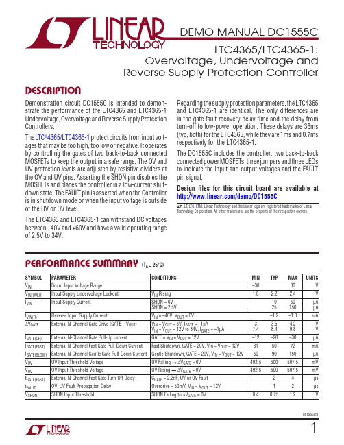
DescriptionOvervoltage, Undervoltage and Reverse Supply Protection ControllerDemonstration circuit DC1555C is intended to demon-strate the performance of the LTC4365 and LTC4365-1 Undervoltage, Overvoltage and Reverse Supply Protection Controllers.The L TC®4365/LTC4365-1 protect circuits from input volt-ages that may be too high, too low or negative. It operates by controlling the gates of two back-to-back connected MOSFETs to keep the output in a safe range. The OV and UV protection levels are adjusted by resistive dividers at the OV and UV pins. Asserting the SHDN pin disables the MOSFETs and places the controller in a low-current shut-down state. The FAUL T pin is asserted when the Controlleris in shutdown mode or when the input voltage is outside of the UV or OV level.The LTC4365 and LTC4365-1 can withstand DC voltages between –40V and +60V and have a valid operating range of 2.5V to 34V.L, L T, L TC, L TM, Linear Technology and the Linear logo are registered trademarks of Linear Technology Corporation. All other trademarks are the property of their respective owners.performance summary(T A = 25°C)Regarding the supply protection parameters, the LTC4365 and LTC4365-1 are identical. The only differences are in the gate fault recovery delay time and the delay from turn-off to low-power operation. These delays are 36ms (typ, both) for the LTC4365, while they are 1ms and 0.7ms respectively for the LTC4365-1.The DC1555C includes the controller, two back-to-back connected power MOSFETs, three jumpers and three LEDs to indicate the input and output voltages and the FAUL T pin signal.Design files for this circuit board are available at /demo/DC1555CSYMBOL PARAMETER CONDITIONS MIN TYP MAX UNITS V IN Board Input Voltage Range–3030V V IN(UVLO)Input Supply Undervoltage Lockout V IN Rising 1.8 2.2 2.4VI VIN Input Supply Current SHDN = 0VSHDN = 2.5V 102550150µAµAI VIN(R)Reverse Input Supply Current V IN = –40V, V OUT = 0V–1.2–1.8mAΔV GATE External N-Channel Gate Drive (GATE – V OUT)V IN = V OUT = 5V, I GATE = –1µAV IN = V OUT = 12V to 34V, I GATE = –1µA37.43.68.44.29.8VVI GATE(UP)External N-Channel Gate Pull-Up current GATE = V IN = V OUT = 12V–12–20–30µA I GATE(FAST)External N-Channel Fast Gate Pull-Down Current Fast Shutdown, GATE = 20V, V IN = V OUT = 12V315072mA I GATE(SLOW)External N-Channel Gentle Gate Pull-Down Current Gentle Shutdown, GATE = 20V, V IN = V OUT = 12V5090150µA V UV UV Input Threshold Voltage UV Falling → ΔV GATE = 0V492.5500507.5mV V OV OV Input Threshold Voltage OV Rising → ΔV GATE = 0V492.5500507.5mV t GATE(FAST)External N-Channel Fast Gate Turn-Off Delay C GATE = 2.2nF, UV or OV Fault24µs t FAUL T OV, UV Fault Propagation Delay Overdrive = 50mV, V IN = V OUT = 12V12µs V SHDN SHDN Input Threshold SHDN Falling to ΔV GATE = 0V0.40.75 1.2V1dc1555cfb2dc1555cfboperating principlesThe LTC4365/LTC4365-1 monitors the input rail voltage and disconnects downstream circuits when the input volt-age is too low, too high or negative. The LTC4365 provides accurate overvoltage and undervoltage comparators to ensure that power is applied to the system only if the input supply is within the allowable voltage window. ReverseDemonstration circuit 1555C is easy to set up to evaluate the performance of the LTC4365/LTC4365-1. Refer to Figures 1a and 1b for proper measurement equipment setup and follow the procedure below.Note that the circuit on the DC1555C is optimized for 12V operation. The Si4230 FET limits overvoltage and reverse voltage to 30V and –30V, respectively. Refer to the LTC4365 data sheet for applications optimized for other voltages.Reverse Voltage Tests (Figure 1a)1) Set JP1 to EN.2) Set JP2 and JP3 to CONNECT LED.3) Connect a power supply across V IN and GND in a nega-tive configuration (connect positive rail to GND and negative rail to V IN ).4) Connect voltmeters at the input and output and ammeter in series with supply.5) Ramp supply down to –30V (referenced to GND).6) Verify that the output voltage is between 0V and –0.5V, all LEDs are off, and the input current is <1.8mA. (FET leakage or other board leakage paths can pull V OUT slightly negative, but it will be clamped by the internal protection diode.)7) Ramp supply back to 0V.Quick start proceDuresupply protection circuit automatically isolates the load from negative input voltages.During normal operation, a high voltage charge pump enhances the gate of external N-channel power MOSFETs. The controller consumes 10µA during shutdown and 125µA while operating.Undervoltage/Overvoltage Test (Figure 1b)8) Reverse the polarity of power supply connection across V IN to GND (connect positive rail to V IN and negative rail to GND).9) Ramp supply up to 30V and verify green V IN LED, red FAUL T LED, green V OUT LED, and V OUT according to Table 1 within the various voltage ranges.10) Ramp supply down from 30V down to 0V and verify green V IN LED, red FAUL T LED, green V OUT LED, and V OUT according to Table 1.11) Repeat steps 9 and 10 with 8A load connected acrossV OUT and GND.Table 1V IN V OUT V IN LED V OUT LED FAUL T LED0V to 5.77V = 0V Off/Dim/OnOff On 6.56V to 13.51V = V IN On On Off 15.47V to 30V= 0VOnOffOnJumper Test12) Remove load and set supply to 9V.13) Move jumpers and verify LEDs according to Table 2.Table 2JP1JP2/JP3VIN LED VOUT LED EN CONNECT LED On On DIS CONNECT LEDOn Off ENOpenOffOffQuick start proceDureFigure 1a. Reverse Voltage MeasurementFigure 1b. Undervoltage/Overvoltage Measurement3dc1555cfbparts listITEM QUANTITY REFERENCE DESCRIPTION MANUFACTURERS PART NUMBER 13CLD1, CLD2, CLD3 Current Limiting, Diode SOD-80Central Semi. Corp. CCLM2000 TR 20C1 (OPT)Cap., X5R 4.7µF 50V 20% 1210Taiyo Yuden UMK325BJ475MM-T 30C2 (OPT)Cap., Alum 47µF 35V 10% SANYO 35CE47AX40C3 (OPT)Cap., X7R 1000pF 50V 10% 0805AVX 08055C102KAT1A52D1, D2 LED, GRN Rohm Semi. SML-010FTT86L61D3 LED, RED Rohm Semi. SML-010VTT86L71D4 Diode, 75V/200mW SOD-523Diodes Inc. 1N4148WT80D5 (OPT)Zener Diode, 15V SOD-523Diodes Inc. BZT52C15T #PBF90D6 (OPT)Zener Diode, 20V POWERDI-123Diodes Inc. DFLT20A #PBF100D7 (OPT)Zener Diode, 40V POWERDI-123Diodes Inc. DFLT40A #PBF114E1, E2, E6, E7 Turret, Testpoint Mill Max 2501-2-00-80-00-00-07-0 124E3, E4, E5, E8 Turret, Testpoint Mill Max 2308-2-00-80-00-00-07-0 133JP1, JP2, JP3 Headers, Single Row 3 Pins 2mm Ctrs.SULLINS NRPN031PAEN-RC141Q1 Dual N-Channel, 30V SO-8Vishay Si4214DY-T1-GE3(AL T) Vishay SI4230DY-T1-GE3 150Q2 (OPT)Dual N-Channel, Low Current SOT-563 Diodes Inc. 2N7002V-7161R1 Res., Chip 1M 0.1W 1% 0603Vishay CRCW06031M00FKEA171R2 Res., Chip 54.9K 0.1W 1% 0603Vishay CRCW060354K9FKEA181R3 Res., Chip 36.5K 0.1W 1% 0603Vishay CRCW060336K5FKEDA191R4 Res., Chip 510K 0.1W 5% 0603Vishay CRCW0603510KJNEA203XJP1, XJP2, XJP3 Shunt, 2mm Ctrs.Samtec 2SN-BK-G214Stand-Off, Nylon 0.25" Tall Keystone, 8831(Snap On)221U1I.C., Overvoltage, Undervoltage and Reverse SupplyLinear Technology Corp. LTC4365CTS8Protection Controller for DC1555C-ALinear Technology Corp. LTC4365CTS8-1 221U1I.C., Overvoltage, Undervoltage and Reverse SupplyProtection Controller for DC1555C-B4dc1555cfb5dc1555cfbInformation furnished by Linear Technology Corporation is believed to be accurate and reliable. However, no responsibility is assumed for its use. Linear Technology Corporation makes no representa-tion that the interconnection of its circuits as described herein will not infringe on existing patent rights.schematic Diagram6dc1555cfbLinear Technology Corporation1630 McCarthy Blvd., Milpitas, CA 95035-7417(408) 432-1900 ● FAX : (408) 434-0507 ● www.linear .comLINEAR TECHNOLOGY CORPORA TION 2011LT 0713 REV B • PRINTED IN USADEMONSTRATION BOARD IMPORTANT NOTICELinear Technology Corporation (L TC) provides the enclosed product(s) under the following AS IS conditions:This demonstration board (DEMO BOARD) kit being sold or provided by Linear Technology is intended for use for ENGINEERING DEVELOPMENT OR EVALUATION PURPOSES ONL Y and is not provided by L TC for commercial use. As such, the DEMO BOARD herein may not be complete in terms of required design-, marketing-, and/or manufacturing-related protective considerations, including but not limited to product safety measures typically found in finished commercial goods. As a prototype, this product does not fall within the scope of the European Union directive on electromagnetic compatibility and therefore may or may not meet the technical requirements of the directive, or other regulations.If this evaluation kit does not meet the specifications recited in the DEMO BOARD manual the kit may be returned within 30 days from the date of delivery for a full refund. THE FOREGOING WARRANTY IS THE EXCLUSIVE WARRANTY MADE BY THE SELLER TO BUYER AND IS IN LIEU OF ALL OTHER WARRANTIES, EXPRESSED, IMPLIED, OR STATUTORY, INCLUDING ANY WARRANTY OF MERCHANTABILITY OR FITNESS FOR ANY PARTICULAR PURPOSE. EXCEPT TO THE EXTENT OF THIS INDEMNITY, NEITHER PARTY SHALL BE LIABLE TO THE OTHER FOR ANY INDIRECT , SPECIAL, INCIDENTAL, OR CONSEQUENTIAL DAMAGES.The user assumes all responsibility and liability for proper and safe handling of the goods. Further , the user releases L TC from all claims arising from the handling or use of the goods. Due to the open construction of the product, it is the user’s responsibility to take any and all appropriate precautions with regard to electrostatic discharge. Also be aware that the products herein may not be regulatory compliant or agency certified (FCC, UL, CE, etc.).No License is granted under any patent right or other intellectual property whatsoever. L TC assumes no liability for applications assistance, customer product design, software performance, or infringement of patents or any other intellectual property rights of any kind.L TC currently services a variety of customers for products around the world, and therefore this transaction is not exclusive .Please read the DEMO BOARD manual prior to handling the product . Persons handling this product must have electronics training and observe good laboratory practice standards. Common sense is encouraged .This notice contains important safety information about temperatures and voltages. For further safety concerns, please contact a L TC applica-tion engineer .Mailing Address:Linear Technology 1630 McCarthy pitas, CA 95035Copyright © 2004, Linear Technology Corporation。
基于LTC4151的汽车过载监控电源接口设计

没启 动 的情 况 下 主要 依 靠 蓄 电 池供 电 的. 载 附 车 件 的功耗增 加 , 必 会 引起 过 载故 障频 发 . 种 不 势 这 确定 的 电压 下跌 或 浪 涌现 象 , 可 能 会 影 响 到 电 有 动助力 系统 ( P ) 汽车核 心 电气设备 的供 电 , E S等 从
而导致 更 为严 重 的行 车安 全 事 故 . 了保 证 汽 车 为
流 的专用 功 率 检 测 芯 片 L 4 5 TC 1 1作 为 功 率 监 控 的主要部 件 , 效 的解 决 了汽 车这 种 高 瞬 变 环 境 有
中的电源 功 率 检 测 , 化 了相 应 的 电压 和 电流 检 简
摘 要 : 绍 了 一款 具 备 输 出功 率 监 控 的汽 车 电源 接 口的 设 计 . 计 中采 用 了宽 范 围 、 直 流 电压 输 入 的专 用 介 设 高
功 率 检 测 芯 片 L C 11作 为 功 率 采 集 核 心 部 件 , 微 控 制 器 的 管 理 下 对 输 出 功 率 测 量 、 断 并 作 出 报 警 处 T 45 在 判
基于 L C 的汽车过载监控 电源接 口设计 T 4 11 5
刘 宋 罗 庚 , 元 礼华 , 俊杰 , 继 黄 峰。
(. 江丹江 口铝业 有 限责任公 司, 1汉 湖北 丹 江 口,4 7 0 42 0 ;
2 黄 石 市有 色机 电设备 制造 公 司 , 北 黄 石 4 5 0 ; . 湖 3 0 5 3 武汉 工程 大学 电气信 息学 院 , . 湖北 武 汉 4 0 电路 简洁 、 可靠.
的安 全运 行 , 有 必 要 对 其 扩 展 的 用 电附 件 的 功 就
LTC4156EUFD#TRPBF;LTC4156IUFD#TRPBF;LTC4156EUFD#PBF;LTC4156IUFD#PBF;中文规格书,Datasheet资料

Management n USB On-The-Go Power Delivery to the USB Port n Four Float Voltage Settings (3.45V, 3.55V, 3.6V, 3.8V) n 28-Lead 4mm × 5mm QFN Package
The LTC4156 is available in the low profile (0.75mm) 28-lead 4mm × 5mm QFN surface mount package.
TYPICAL ቤተ መጻሕፍቲ ባይዱPPLICATION
I2C Controlled High Power Battery Charger/USB Power Manager
4156 TA01b
4156f
1
LTC4156 TABLE OF CONTENTS
Features............................................................................................................................. 1 Applications........................................................................................................................ 1 Typical Application ................................................................................................................ 1 Description......................................................................................................................... 1 Absolute Maximum Ratings...................................................................................................... 3 Order Information.................................................................................................................. 3 Pin Configuration.................................................................................................................. 3 Electrical Characteristics......................................................................................................... 4 Typical Performance Characteristics........................................................................................... 9 Pin Functions......................................................................................................................12 Block Diagram.....................................................................................................................15 Timing Diagrams.................................................................................................................16 Operation.......................................................................................................................... 17
LTC4054
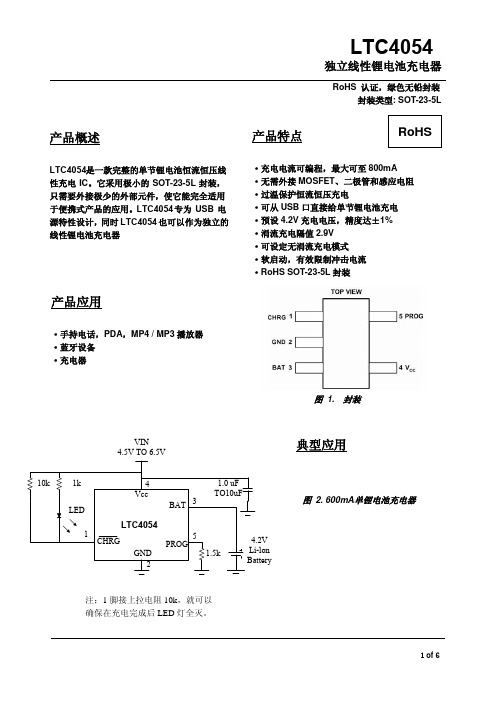
产品特点·充电电流可编程,最大可至800mA ·无需外接MOSFET 、二极管和感应电阻 ·过温保护恒流恒压充电·可从USB 口直接给单节锂电池充电 ·预设4.2V 充电电压,精度达±1% ·涓流充电隔值2.9V ·可设定无涓流充电模式 ·软启动,有效限制冲击电流 ·RoHS SOT-23-5L 封装RoHS 认证,绿色无铅封装封装类型: SOT-23-5L产品应用·手持电话,PDA ,MP4 / MP3播放器 ·蓝牙设备 ·充电器图 1. 封装产品概述 典型应用图 2. 600mA 单锂电池充电器LTC4054是一款完整的单节锂电池恒流恒压线性充电IC 。
它采用极小的SOT-23-5L 封装,只需要外接极少的外部元件,使它能完全适用于便携式产品的应用。
专为USB 电源特性设计,同时 也可以作为独立的线性锂电池充电器 CHRGVIN 4.5V TO 6.5V注:1脚接上拉电阻10k ,就可以 确保在充电完成后LED 灯全灭。
LTC4054LTC4054LTC4054管脚描述CHRG(1):开漏极充电状态输出脚。
当对电池充电时,内部NMOS管将此引脚拉低,充电状态指示LED 亮;当充电完成时,内部NMOS管为高阻态,LED灭。
GND(2):电源地。
BAT(3):充电电流输出脚。
向电池提供充电电流,同时控制充电完成电压为4.2V。
内部精确电阻分压器从改脚引出,控制输出电压。
关断模式下,此电阻分压器从改脚断开连接。
VCC(4):电源输入正极。
向充电器供电,电压范围4.5V至6.5V。
接1μF对地电容以减少纹波。
PROG(5):充电电流编程器脚,充电电流监测与充电开关。
可通过此脚与地之间链接的1%电阻来设定充电电流。
当芯片处于恒流充电状态时,此脚上的电平定义为1V。
所有工作状态下,充电电流的大小可按下式计算:I BAT = 900V PROG / R PROG此脚也可作为充电开关脚,将此脚和地断开,充电器进入关断模式,充电停止,芯片的输入电流降至25μA以下。
锂电池线性充电管理芯片LTC4065及其应用
锂电池线性充电管理芯片LTC4065及其应用随着移动计算技术和无线通信技术的发展,微型移动终端设备在移动数据采集、传输、处理及个人信息服务等领域得到越来越多的应用。
锂电池因其体积小、能量密度高、无记忆效应、循环寿命高、高电压电池和自放电率低等优点,近年来已经成为微型移动终端设备的首选电源。
锂电池的特性以及应用环境的需求,对微型移动终端设备充电方案的设计提出了更高的要求。
因此在充电方案的设计中需要综合考虑成本、体积、噪声、效率等因素。
[1] LTC4065是一款用于单节锂电池的完整恒定电流/恒定电压线性充电管理芯片,可提供高达750 mA且准确度为5%的可设置的充电电流,并支持直接使用USB端口对单节锂电池进行充电。
同时其热反馈功能可调节充电电流,以便在大功率工作或高环境温度条件下对芯片温度加以限制,确保安全工作。
由于采用了内部MOSFET架构,因此无需使用外部检测电阻器或隔离二极管。
很少的外部元件数目加上其2 mm×2 mm DFN封装,使得LTC4065尤其适合无线PDA、蜂窝电话、无线传感器终端等应用。
功能齐全的LTC4065还包括自动再充电、低电池电量充电调节、软启动等丰富功能。
图1 LTC4065芯片引脚排列1 LTC4065的引脚功能LTC4065采用了热处理能力较强的6引脚小外形封装(DFN),且实现产品无铅化,底部采用裸露衬垫,直接焊接至PCB以实现电接触和额定散热性能。
引脚排列如图1所示。
各引脚功能如下:引脚1,GND,接地端。
引脚2,CHRG,漏极开路充电状态输出。
充电状态指示引脚具有三种状态:下拉、2 Hz脉动和高阻抗状态。
该输出可以被用作一个逻辑接口或一个LED驱动器。
对电池进行充电时,有一个内部N沟道MOSFET将GHRG引脚拉至低电平。
当充电电流降至全标度电流的10%时,CHRG 引脚被强制为高阻抗状态。
如果电池电压处于2.9 V以下的持续时间达到充电时间的1/4,则认为电池失效,而且CHRG引脚将以2 Hz的频率脉动。
LTC4054USB锂电充电芯片

功能描述LTC4054(LTH7)是一款完整的单节锂电池恒流线性充电IC,只需要极少的外部元件,专为USB电源特性设计,同时4054也可以作为独立的线性锂电池充电器,LTC4054充电饱和灯是微灭的。
得益于内部的MOSFET 结构,在应用上不需要外部电阻和阻塞二极管。
在高能量运行和高外围温度时,热反馈可以控制充电电流以降低芯片温度。
LTC4054充电电压被限定在,充电电流通过外部电阻调节。
在达到目标充电电压后,当充电电流降低到设定值的1/10 时,LTC4054就会自动结束充电过程。
当输入端(插头或USB 提供电源)拔掉后,LTC4054 自动进入低电流状态,电池漏电流将降到2μA以下。
LTC4054还可被设置于停止工作状态,使电源供电电流降到25μA。
其余特性包括:充电电流监测,输入低电压闭锁,自动重新充电和充电已满及开始充电的标志。
LTC4054(LTH7)采用SOT23-5、SOT89-5以及客户订制的封装形式,广泛应用于手机、PDA、MP3及蓝牙产品方面。
LTC4054(LTH7)
产品特性可编程使充电电流可达800mA. 不需要MOSFET,传感电阻和阻塞二极管小的尺寸实现对锂离子电池的完全线形充电管理恒电流/恒电压运行和热度调节使得电池管理效力最高,没有热度过高的危险从USB 接口管理单片锂离子电池预设充电电压为±1% 充电电流输出监控充电状态指示标志1/10 充电电流终止停止工作时提供25μA 电流涓流充电阈值电压软启动限制浪涌电流电流。
- 1、下载文档前请自行甄别文档内容的完整性,平台不提供额外的编辑、内容补充、找答案等附加服务。
- 2、"仅部分预览"的文档,不可在线预览部分如存在完整性等问题,可反馈申请退款(可完整预览的文档不适用该条件!)。
- 3、如文档侵犯您的权益,请联系客服反馈,我们会尽快为您处理(人工客服工作时间:9:00-18:30)。
1.21k 499Ω
47nF
4155 TA01a
EFFICIENCY (%)
Switching Regulator Efficiency
100 90
80
70 60
50
40
30
20
10 VBAT = 3.9V
0 0 0.5 1.0 1.5 2.0 2.5 3.0 3.5
LOAD CURRENT (A)
I2C ........................................................................................................................................................................ 17 Applications Information .......................................................................................................40 Typical Applications .............................................................................................................47 Package Description ............................................................................................................51 Typical Application ..............................................................................................................52 Related Parts .....................................................................................................................52
n Monolithic Switching Regulator Makes Optimal Use of Limited Power and Thermal Budget
n Dual-Input Overvoltage Protection Controller n Priority Multiplexing for Multiple Inputs n I2C/SMBus Control and Status Feedback n NTC Thermistor ADC for Temperature Dependent
Four Float Voltage Settings n 28-Lead 4mm × 5mm QFN Package
APPLICATIONS
n Tablet PCs n Ultra Mobile PCs n Video Media Players n Digital Cameras, GPS, PDAs n Smart Phones n Portable Medical Devices
I2C adjustability of input current, charge current, battery float voltage, charge termination, and many other parameters allows maximum flexibility. I2C status reporting of key system and charge parameters facilitates intelligent control decisions. USB On-The-Go support provides 5V power back to the USB port without any additional components. A dual-input, priority multiplexing, overvoltage protection circuit guards the LTC4155 from high voltage damage on the VBUS pin.
DESCRIPTION
The LTC®4155 is a 15 watt I2C controlled power manager with PowerPath™ instant-on operation, high efficiency switching battery charging and USB compatibility. The LTC4155 seamlessly manages power distribution from two 5V sources, such as a USB port and a wall adapter, to a single-cell rechargeable Lithium-Ion/Polymer battery and a system load.
The LTC4155’s switching battery charger automatically limits its input current for USB compatibility, or may draw up to 3A from a high power wall adapter. The high efficiency step-down switching charger is designed to provide maximum power to the application and reduced heat in high power density applications.
WALLSNS WALLGT
1μH SW
VOUT
TO SYSTEM LOAD
VIN
VBUS
10μF
CHGSNS
LTC4155
BATGATE
22μF
USBGT
BATSNS
3.6k
100k
USBSNSNTCBFra bibliotekASID
NTC
3 I2C IRQ GND CLPROG2 CLPROG1 PROG VC OVGCAP
L, LT, LTC, LTM, Linear Technology and the Linear logo are registered trademarks and PowerPath and Bat-Track are trademarks of Linear Technology Corporation. All other trademarks are the property of their respective owners.
4155 TA01b
4155fc
1
LTC4155 TABLE OF CONTENTS
Features ............................................................................................................................ 1 Applications ....................................................................................................................... 1 Typical Application ............................................................................................................... 1 Description......................................................................................................................... 1 Absolute Maximum Ratings..................................................................................................... 3 Order Information................................................................................................................. 3 Pin Configuration ................................................................................................................. 3 Electrical Characteristics ........................................................................................................ 4 Typical Performance Characteristics .......................................................................................... 9 Pin Functions .....................................................................................................................12 Block Diagram....................................................................................................................15 Timing Diagrams ................................................................................................................16 Operation.......................................................................................................................... 17