TLE4921-5U pdf
SI4925中文资料

-0.73
-1.2
1. RθJA is the sum of the junction-to-case and case-to-ambient thermal resistance where the case thermal reference is defined as the solder mounting surface of the drain pins. RθJC is guaranteed by design while RθCA is determined by the user's board design.
ON CHARACTERISTICS
Gate Threshold Voltage Gate Threshold Voltage Temp. Coefficient Static Drain-Source On-Resistance
∆VGS(th)/∆TJ
RDS(ON)
Ω
ID(ON) gFS Ciss Coss Crss tD(on) tr tD(off) tf Qg Qgs Qgd IS VSD
1.4
I D= -6A VGS = -10V
I D = -3A
0.08
R DS(ON) , NORMALIZED
1.2
0.06
1
0.04
TA = 125°C 25° C
0.8
0.02
0.6 -50
-25
0
25
50
75
100
125
150
0
2
TJ , JUNCTION TEMPERATURE (° C)
SOT-23
SuperSOTTM-6
霍尔IC著名厂家产品功能特性汇总(MELEXIS, ALLEGRO, INFENION,AKM, HONEYWELL)

ALLEGRO品牌霍尔专区Allegro MicroSystems 公司在高性能电源和霍尔效应传感器集成电路的开发、制造及营销领域始终引领全球潮流。
Allegro 独具创新的解决方案服务于汽车市场中的高增长应用,此外也开发办公自动化、工业和消费通讯解决方案。
Allegro 主要为电动机控制、调节及磁场感测应用开发集成电路解决方案。
提供高度集成的混合信号IC,不仅元件数量日益增多,功能也更加强大。
A1201参数下载A1202参数下载A1203参数下载A1204参数下载A1205参数下载A1101参数下载A1102参数下载A1103参数下载A1104参数下载A1106参数下载A1321参数下载A1322资料下载A1323参数下载A1642参数下载A3121参数下载A3187参数下载A3212参数下载A3240参数下载A3280参数下载A3282参数下载A3955参数下载A3977参数下载A8904参数下载ACS712参数下载ACS712参数下载ACS712参数下载ATS616参数下载ATS674参数下载注:点击霍尔型号查看详细参数MELEXIS品牌霍尔专区来源: 发布时间: 2012-04-11 00:13 1579 次浏览大小: 16px 14px 12px MELEXIS公司是一家专业的集成电路公司,10多年来,Melexis公司已开发出世界一流的,创新的混合信号半导体,依靠优秀的技术,在霍尔IC的研发能力和速度在业内是屈指可数的,在降低系统成本和产品设计的灵活性和优越的霍尔质量可靠性方面具有很大的MELEXIS公司是一家专业的集成电路公司,10多年来,Melexis公司已开发出世界一流的,创新的混合信号半导体,依靠优秀的技术,在霍尔IC的研发能力和速度在业内是屈指可数的,在降低系统成本和产品设计的灵活性和优越的霍尔质量可靠性方面具有很大的竞争优势。
在全球的各种汽车品牌中基本上都有Melexis设计研发的霍尔集成电路。
HA469255U001版本4技术手册说明书
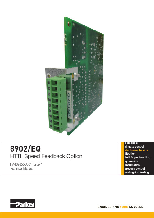
8902/EQHTTL Speed Feedback Option HA469255U001 Issue 4Technical Manual8902/EQHTTL Speed Feedback OptionTechnical ManualHA469255U001 Issue 4Compatible with Version 1.x Software© Copyright 2011 Parker SSD Drives, a division of Parker Hannifin Ltd.All rights strictly reserved. No part of this document may be stored in a retrieval system, or transmitted in any form or by any means to persons not employed by a Parker SSD Drives company without written permission from Parker SSD Drives, a division of Parker Hannifin Ltd . Although every effort has been taken to ensure the accuracy of this document it may be necessary, without notice, to make amendments or correct omissions.Parker SSD Drives cannot accept responsibility for damage, injury, or expenses resulting therefrom.WARRANTYParker SSD Drives warrants the goods against defects in design, materials and workmanship for the period of 12 months from the date of delivery on the terms detailed in Parker SSD Drives Standard Conditions of Sale IA500504.Parker SSD Drives reserves the right to change the content and product specification without notice.Cont.1WARNING!During commissioning, remove the fuses (or trip the circuit breaker) on your 3-phase supply.Make sure the power is OFF, and that it cannot be switched on accidentally whilst youare working.REFER TO YOUR MAIN PRODUCT MANUAL FOR SPECIFIC SAFETYINFORMATION ABOUT THE DEVICE YOU ARE CONTROLLING IMPORTANT:Please read this information BEFORE installing the equipment.Intended UsersThis manual is to be made available to all persons who are required to install, configure orservice equipment described herein, or any other associated operation.The information given is intended to highlight safety issues, EMC considerations, and to enablethe user to obtain maximum benefit from the equipment.Application AreaThe equipment described is intended for industrial motor speed control.PersonnelInstallation, operation and maintenance of the equipment should be carried out by qualifiedpersonnel. A qualified person is someone who is technically competent and familiar with allsafety information and established safety practices; with the installation process, operation andmaintenance of this equipment; and with all the hazards involved.SafetyAll control and signal terminals are SELV, i.e. protected by double insulation.EMCIn a domestic environment this product may cause radio interference in which case the user maybe required to take adequate counter-measures.This equipment contains electrostatic discharge (ESD) sensitive parts. Observe static controlprecautions when handling, installing and servicing this product.Cont.2CAUTION!At any time, there may be a loss of motor control and separate/independent application measures should be taken to ensure that such loss of motor control cannot present a safety hazard.RISK ASSESSMENTUnder fault conditions, power loss or unintended operating conditions, the drive may not operate as intended. In particular:•Stored energy might not discharge to safe levels as quickly as suggested, and can still be present even though the drive appears to be switched off •The motor's direction of rotation might not be controlled•The motor speed might not be controlled •The motor might be energisedA drive is a component within a drive system that may influence its operation or effects under a fault condition. Consideration must be given to:•Stored energy •Supply disconnects •Sequencing logic •UnintendedoperationCont.3ContentsContents PageCont.41 Description (1)•Features (1)•Part Number (1)•Used On (1)•Specifications (1)Recommended Spare Parts (1)DIP Switch Settings (2)Installation (3)Fitting the Option (3)Wiring the System (5)•X34 Connections (5)Initial Set-up (6)Configuring the 890 Drive (6)•ENCODER Function Block (6)Parker SSD Drives Approved Encoders (8)1DescriptionThe HTTL Speed Feedback Option allows incremental encoders to be connected directly to themotor controller to provide highly accurate speed feedback measurement.FeaturesThe option has the following features:•Contains three optically isolated differential inputs on channels A, B and M•Decoding logic to interface the encoder to the microprocessor•Supplies variable voltage, isolated encoder power supplyPart NumberThe part number for the HTTL Speed Feedback Option is:8902-EQ-00-008902-EQ-00-FF (indicates a factory-fitted option)Used OnThis option can be used on 890 drives with the following Product Codes:890SD-.. 890SD Standalone Drive890CD-.. 890CD Common Bus DriveRefer to the 890 Engineering Reference Manual, Appendix E for Product Code details.SpecificationsMaximum Pulse Rate 250kHz (differential)200kHz (single-ended)Receiver Current ≤10mA per channelInput Format Two differential channels in quadrature,clock/dir or clock onlyInput Voltage Range ±30V (differential)0-30V (single-ended)Input Voltage Threshold 3V ± 1V (differential)8V ± 1V (single-endedl)Encoder Supply Maximum load = 200mA or 2W, whicheveris smaller. Voltage adjustable 10-20V byfirmwareTerminal Wire Size (maximum) 16 AWGTerminal Tightening Torque 0.22 - 0.25Nm (1.9 - 2.2 pound-inches)Recommended Spare PartsWe recommend that you keep one option as a spare to reduce down-time.8902/EQ HTTL Speed Feedback Option28902/EQ HTTL Speed Feedback OptionDIP Switch SettingsThe switch settings control the following inputs:Usually the switches will be set to give a threshold of 3V when using a differential encoder, and to 8V when using a single-ended encoder. (Factory default is with all switches set in the ON position - 3V).DIP SWITCHInput ThresholdSwitch Number 1 2 3 4 Input ControlledABMnot used3V±1 On On On On 8V±1 Off Off Off Off Figure 1 Option board showingDIP Switch location38902/EQ HTTL Speed Feedback OptionFigure 3 Rear ofControl BoardFigure 2 Control board showing Option correctly mountedABBInstallationFitting the OptionIf the option is not factory-fitted, follow the procedure given below.WARNING!Disconnect all sources ofpower before attemptinginstallation.CautionThis option contains ESD(Electrostatic Discharge) sensitiveparts. Observe static controlprecautions when handling,installing and servicing this option.The Control Card assembly needs to beremoved from the drive as follows tofit the Option in “OPTION F” position.1.Undo the two screws securingOption A and Option B to the frontof the drive. If options are notfitted, completely remove theblank covers for the Option A andOption B slots.2.Undo the captive screws (A)located in the top and bottomhandles of the control board.Gently pull on the handles towithdraw the board from the drive,supporting any attached optionboards. Note that the boards aresliding in top and bottom slots.3.If fitted, remove Option A and/or B boards that aremounted on the control board by separating theconnector at the rear of the option board from thecontrol board.4.Remove the blanking plate from “OPTION F” location(2 screws).5.Remove the terminal block from the HTTL Option.6.Offer up the HTTL Option through the "OPTION F"cut-out as shown opposite. Fit the two locating pegs ofthe large connector on the rear edge of the optionboard into the locating holes on the control board, asshown opposite.7.Fit the two screws and crinkle washers (C) at the rearedge of the Option.DO NOT OVERTIGHTEN.Tightening torque : 0.2Nm (28 oz-in).Ensure locating pegs are correctly located visablythrough locating holes.48.Secure with the two screws (B) to the front of the control board.Ensure ‘C’ screws to option connector have been fully tightened before fitting ‘B’ screws.The front panel screws (B) are self-tapping and can be quite hard to turn. This turningtorque must not be transferred through the option board to the control board connector.To avoid this hold the option board with one hand, while tightening the front panel screwswith the other. DO NOT hold the control board while tightening these screws.9.Re-fit terminal block to the HTTL Option.10.Refit Options A and B: Press the assembly into the connector on the Control Board. Ensurethat the front panel of the TechCard overlaps the front of the Control Board. Ease theconnector at the TechCard so that the two PCB's are parallel when viewed on edge.11.Replace the control board (with attached options) into the drive. Tighten screws (A).12.Tighten the Option A and Option B screws; or importantly, fit the blank covers and securewith the screws. If Options are not fitted.8902/EQ HTTL Speed Feedback Option58902/EQ HTTL Speed Feedback OptionWiring the SystemWARNING!Disconnect all sources of power before attempting installation.CautionThis option contains ESD (Electrostatic Discharge) sensitive parts. Observe static controlprecautions when handling, installing and servicing this option.X34 ConnectionsFor correct operation, A, /A, B and /B must be connected as shown. If any is left unconnected, the HTTL speed feedback option will not operate.The M input is not normally connected - it is for use with future versions of the drive software.M: for connection to the once-per-revolution marker output from the encoder to verify correct operation of the encoder.Take special care wiring the encoders to the Option due to the low level of the signals. Use twisted-pair, screened cable, preferably with an overall screen and a screen over each individual pair. To ensure compliance with the EMC Directive the overall cable screen should be connected to the encoder body and to the cable clamp. Recommended cable:3 pairs individually screened, plus overall screen, characteristic impedance 100 to 120Ω, e.g. Belden 81631 GND2 -V3 +V4 /M5 M6 /B7 B8 /A9 AX34X34TerminalSingle-Ended Encoder OutputsDifferential Encoder OutputsFigure 4 Wiring Diagram68902/EQ HTTL Speed Feedback OptionInitial Set-upConfiguring the 890 DriveUse the DSE 890 Configuration Tool to configure the ENCODER function block, as detailed below.Note:The DSE 890 Configuration Tool is Parker SSD Drives’ Windows-based block programming software and is supplied with each drive.ENCODER Function BlockSETUP::MOTOR CONTROL::ENCODERThis block allows Speed Feedback to be measured using a quadrature pulse encoder. Parameter DescriptionsPULSE ENC VOLTSPREF: 71.01 Default: 10.0 V Range: 10.0 to 20.0 V Set this approximately to the supply voltage required by the pulse encoder.SINCOS ENC VOLTS PREF: 71.22Default: 5.0 V Range: See below Set the supply volts required by the sin/cos encoder. Enumerated Value : SinCos Encoder Volts0 : 5V 1 : 10VENCODER LINESPREF: 71.02 Default: 2048 Range: 250 to 262143 Set the number of lines to match the type of encoder being used. Incorrect setting of this parameter will result in an erroneous speed measurement.ENCODER INVERTPREF: 71.03 Default: FALSE Range: FALSE/TRUE Used to match the encoder direction to the motor direction. When TRUE, changes the sign of the measured speed and the direction of the position count. Setting the encoder direction should be done as part of the Autotune when running in Closed-loop Vector Mode.LOAD G'BOX RATIO PREF: 71.05Default: 1 Range: 1 to 64 This parameter can be used to configure absolute position control applications. It must be aninteger gear box ratio, e.g. 64:1. If there is a gearbox between the motor and the load, set the gearbox ratio via this parameter. “LOAD POSITION” i.e. the position of the load on the other side of the gearbox, will then be calculated.ENCODER MECHO/SPREF: 71.06 Default: 0.0000 deg Range: 0.0000 to 360.0000 deg (encoder mechanical offset)Use this parameter ro enter a mechanical offset of between 0 and 360 degrees to allow the output shaft position to be correctly zeroed. This value is subtracted from the LOAD POSITION which is reported by the encoder.To zero the shaft position: turn the shaft to the zero position; note the value of the LOAD POSITION parameter, and enter this value into the ENCODER MECH O/S parameter. LOAD POSITION will now read zero.Note that “load position” refers here to the shaft position on the other side of a gearbox which may be mounted on the motor output. It does not refer to the motor shaft position, unless the output gearbox ratio (LOAD G'BOX RATIO) is set to 1 (i.e. no gearbox fitted).ENCODER FBK %PREF: 71.08 Default: —.xx % Range: —.xx % This parameter shows the mechanical speed of the motor shaft, calculated from the encoderfeedback, as a percentage of the user maximum speed setting (MAX SPEED in the REFERENCE function block).SHAFT POSITIONPREF: 71.09Default: —.xx degRange: —.xx degThis diagnostic provides the motor shaft position (before the gear box).Ignore the setting for this parameter78902/EQ HTTL Speed Feedback OptionParameter DescriptionsLOAD POSITIONPREF: 71.10 Default: —.xx degRange: —.xx degThis is the position of a shaft on the other side of a gearbox attached to the motor. If a gearboxis not fitted, set LOAD G'BOX RATIO to 1. This variable is controlled by the position loop, i.e. the position loop will force the load position to equal the demanded position.ENCODER TYPEPREF: 71.04 Default: 0 Range: See below This parameter defines the type of encoder being used.A wrt /AB wrt /BQuadrature and Quadrature Diffdirection = forward direction = reverse(assumes ENCODER INVERT is FALSE)A wrt /AB wrt /BClock/Dir and Clock/Dir Diffdirection = forward direction = reverse(assumes ENCODER INVERT is FALSE)A wrt /AB wrt /B Clock and Clock Diffdirection = forward (assumes ENCODER INVERT is FALSE)direction = forward(ignored)Enumerated Value : Type0 : QUADRATURE single-ended pulse encoder 1 : CLOCK/DIR single-ended pulse encoder 2 : CLOCK single-ended pulse encoder 3 : QUADRATURE DIFF differential pulse encoder 4 : CLOCK/DIR DIFF differential pulse encoder 5 : CLOCK DIFF differential pulse encoder 6 : SINCOS INC sin/cos encoder 7 : ABS ENDAT STsingle turn endat absolute encoder 8 : ABS ENDAT MT multi-turn endat absolute encoderSave the ApplicationRemember to save your new configuration in DSE 890 and install it in the drive. In DSE 890, select "Command ÆInstall At Selected" to install the currently opened configuration into a drive.88902/EQ HTTL Speed Feedback OptionParker SSD Drives Approved EncodersHengstler: RI 58TD//2048ED.37IFRecommended Encoder (12mm bore)SSD Drives Part Number: DD464475U012BEI(HS35 series):924-01070-279, -283, -281 Recommended Encoder (North America)(Hollow Shaft, Various Bores) SSD Drives Part Number:Frame Designs: TENV, TEBC, TEFCDD470666, DD470667, DD471123Hengstler: RI 76TD/2048ED-4N20IF Alternative Encoders (20mm bore)SSD Drives Part Number:DD464475U020Encoders are available from Hengstler or BEI in other accuracies such as 500 lines/rev or 2000lines/rev to suit the application.05/03/09 CANADAParker Hannifi n CanadaMotion & Control Division160 Chisholm DriveMilton, Ontario L9T 3G9Tel: +1(905) 693-3000Fax: +1(905) 876-1958GERMANYParker Hannifi n GmbHVon-Humboldt-Strasse 1064646 HeppenheimTel: +49 (6252) 798200Fax: +49(6252) 798205CHINAParker Hannifi n Motion & Control(Shanghai) Co. Ltd.,280 Yunqiao RoadJinqiao Export Processing Zone,Pudong District, Shanghai 201206Tel: +86(21) 5031 2525Fax: +86(21) 5854 7599ITALYParker Hannifi n SPAVia C. Gounod, Cinisello Balsamo1-20092, MilanoTel: +39(0236) 1081Fax: +39(0236) 108400FRANCEParker SSD Parvex8 Avenue du LacB.P. 24921007 Dijon CedexTel: +33(0)3 80 42 41 40Fax: +33(0)3 80 42 41 23USAParker Hannifi n CorporationSSD Drives9225 Forsyth Park DriveCharlotteNorth Carolina 28273Tel: +1(704)588 3246Fax: +1(704)588 3249Argentina • Australia • Austria • Bangladesh • Belgium • Brazil • Chile • Columbia • Costa Rica • Cyprus • Czech Republic • Denmark • Ecuador • Egypt • Finland • Greece • Hong Kong • Hungary • India • Indonesia • Iran • Ireland • Israel • Japan • Jordan • Kenya • Korea • Kuwait • Lithuania • Malaysia • Netherlands • New Zealand • Nigeria • Norway • Peru • Philippines • Poland • Portugal • Quatar • Romania • Russia • Saudi Arabia • Singapore • Slovenia • Slovakia • South Africa • Spain • Sri Lanka • Sweden • Switzerland • Taiwan • Turkey • United Arab Emirates * Vietnam • ZimbabweLocal availability and service support also in:Parker Hannifi n Ltd., Automation Group, SSD Drives EuropeNew Courtwick Lane, Littlehampton, West Sussex BN17 7RZUnited Kingdom. Tel: +44(0)1903 737000 Fax: +44(0)903 737100*HA469255U001_04*。
SCI 高性能 NPN 双极性晶体管 2N4921G、2N4922G、2N4923G 数据手册说明书

2N4921G, 2N4922G,2N4923GMedium-Power PlasticNPN Silicon TransistorsThese high−performance plastic devices are designed for driver circuits, switching, and amplifier applications.Features•Low Saturation V oltage•Excellent Power Dissipation•Excellent Safe Operating Area•Complement to PNP 2N4920G•These Devices are Pb−Free and are RoHS Compliant** MAXIMUM RATINGSRating Symbol Value UnitCollector−Emitter Voltage 2N4921G2N4922G2N4923G V CEO406080VdcCollector−Emitter Voltage 2N4921G2N4922G2N4923G V CB406080VdcEmitter Base Voltage V EB 5.0VdcCollector Current − Continuous (Note 1)I C 1.0Adc Collector Current − Peak (Note 1)I CM 3.0Adc Base Current − Continuous I B 1.0AdcTotal Power Dissipation @ T C = 25_C Derate above 25_C PD300.24WmW/_COperating and Storage JunctionTemperature RangeT J, T stg–65 to +150_CStresses exceeding those listed in the Maximum Ratings table may damage the device. If any of these limits are exceeded, device functionality should not be assumed, damage may occur and reliability may be affected.1.The 1.0 A maximum I Cvalue is based upon JEDEC current gain requirements.The 3.0 A maximum value is based upon actual current handling capability of the device (see Figures 5 and 6).THERMAL CHARACTERISTICS (Note 2)Characteristic Symbol Max Unit Thermal Resistance, Junction−to−Case R q JC 4.16_C/W 2.Recommend use of thermal compound for lowest thermal resistance.*Indicates JEDEC Registered Data.*For additional information on our Pb−Free strategy and soldering details, please download the ON Semiconductor Soldering and Mounting Techniques Reference Manual, SOLDERRM/D.1.0 AMPEREGENERAL PURPOSEPOWER TRANSISTORS40−80 VOLTS, 30 WATTSMARKING DIAGRAMY=YearWW=Work Week2N492x=Device Codex = 1, 2, or 3G=Pb−Free PackageDevice Package Shipping ORDERING INFORMATION2N4921G TO−225(Pb−Free)500 Units / Box2N4922G TO−225(Pb−Free)500 Units / Box2N4923G TO−225(Pb−Free)500 Units / Box3EMITTERCOLLECTORTO−225CASE 77−09STYLE 13YWW2N492xGELECTRICAL CHARACTERISTICS (T C= 25_C unless otherwise noted)Characteristic Symbol Min Max Unit OFF CHARACTERISTICSCollector−Emitter Sustaining Voltage (Note 3) (I C = 0.1 Adc, I B = 0)2N4921G2N4922G2N4923G V CEO(sus)406080−−−VdcCollector Cutoff Current (V CE = 20 Vdc, I B = 0)2N4921G(V CE = 30 Vdc, I B = 0)2N4922G(V CE = 40 Vdc, I B = 0)2N4923G I CEO−−−0.50.50.5mAdcCollector Cutoff Current(V CE = Rated V CEO, V EB(off) = 1.5 Vdc)(V CE = Rated V CEO, V EB(off) = 1.5 Vdc, T C = 125_C I CEX−−0.10.5mAdcCollector Cutoff Current (V CB = Rated V CB, I E = 0)I CBO−0.1mAdcEmitter Cutoff Current (V EB = 5.0 Vdc, I C = 0)I EBO− 1.0mAdcON CHARACTERISTICSDC Current Gain (Note 3)(I C = 50 mAdc, V CE = 1.0 Vdc) (I C = 500 mAdc, V CE = 1.0 Vdc) (I C = 1.0 Adc, V CE = 1.0 Vdc)h FE403010−150−−Collector−Emitter Saturation Voltage (Note 3) (I C = 1.0 Adc, I B = 0.1 Adc)V CE(sat)−0.6VdcBase−Emitter Saturation Voltage (Note 3) (I C = 1.0 Adc, I B = 0.1 Adc)V BE(sat)− 1.3VdcBase−Emitter On Voltage (Note 3) (I C = 1.0 Adc, V CE = 1.0 Vdc)V BE(on)− 1.3VdcSMALL−SIGNAL CHARACTERISTICSCurrent−Gain − Bandwidth Product(I C = 250 mAdc, V CE = 10 Vdc, f = 1.0 MHz)f T3.0−MHzOutput Capacitance(V CB = 10 Vdc, I E = 0, f = 100 kHz)C ob−100pFSmall−Signal Current Gain(I C = 250 mAdc, V CE = 10 Vdc, f = 1.0 kHz)h fe25−−Product parametric performance is indicated in the Electrical Characteristics for the listed test conditions, unless otherwise noted. Product performance may not be indicated by the Electrical Characteristics if operated under different conditions.3.Pulse Test: PW ≈ 300 m s, Duty Cycle ≈ 2.0%.40302010255075100125150Figure 1. Power DeratingT C , CASE TEMPERATURE (°C)P D , P O W E R D I S S I P A T I O N (W A T T S )Safe Area Curves are indicated by Figure 5. All limits are applicable and must be observed.Figure 2. Switching Time Equivalent Circuit5.0Figure 3. Turn −On TimeI C , COLLECTOR CURRENT (mA)t , T I M E ( s )μ 2.01.00.70.50.30.20.10.052.0%0.073.0V BE(off)V in V TURN-OFF PULSEobtain desired current levelsFigure 4. Thermal Responset, TIME (ms)1.00.010.70.50.30.20.10.070.050.030.02r (t ), T R A N S I E N T T H E R M A LR E S I S T A N C E (N O R M A L I Z E D )10Figure 5. Active −Region Safe Operating AreaV CE , COLLECTOR-EMITTER VOLTAGE (VOLTS)5.02.01.00.50.10.2I C , C O L L E C T O R C U R R E N T (A M P )7.03.00.70.3There are two limitations on the power handling ability of a transistor: average junction temperature and second breakdown. Safe operating area curves indicate I C − V CE operation i.e., the transistor must not be subjected to greater dissipation than the curves indicate.The data of Figure 5 is based on T J(pk) = 150_C; T C is variable depending on conditions. Second breakdown pulse limits are valid for duty cycles to 10% provided T J(pk) ≤ 150_C. At high case temperatures, thermal limitations will reduce the power that can be handled to values less than the limitations imposed by second breakdown.t μs , S T O R A G E T I M E ( s )′5.0Figure6. Storage Time I C , COLLECTOR CURRENT (mA)2.01.00.50.30.20.10.050.073.00.75.0Figure 7. Fall TimeI C , COLLECTOR CURRENT (mA)2.01.00.50.30.20.10.050.073.00.7t μf , F A L L T I M E ( s )V C E , C O L L E C T O R -E M I T T E R V O L T A G E (V O L T S )R B E , E X T E R N A L B A S E -E M I T T E R R E S I S T A N C E (O H M S )1000Figure 8. Current GainI C , COLLECTOR CURRENT (mA)1050020010070Figure 9. Collector Saturation Region1.0I B , BASE CURRENT (mA)0.80.60.40.2700300h F E , D C C U R R E N T G A I N503020108Figure 10. Effects of Base −Emitter Resistance T J , JUNCTION TEMPERATURE (°C)1071051041031061.5I C , COLLECTOR CURRENT (mA)1.20.90.60.3V O L T A G E (V O L T S )Figure 11. “On” Voltage104Figure 12. Collector Cut −Off Region V BE , BASE-EMITTER VOLTAGE (VOLTS)10310210-1, C O L L E C T O R C U R R E N T ( A )μI C + 2.5Figure 13. Temperature CoefficientsI C , COLLECTOR CURRENT (mA)T E M P E R A T U R E C O E F F I C I E N T S (m V /C )°+ 2.0+ 1.5+ 0.50- 0.5- 1.0- 1.5- 2.0- 2.5+ 1.010110010- 2TO −225CASE 77−09ISSUE ADDATE 25 MAR 2015STYLE 1:PIN 1.EMITTER 2., 4.COLLECTOR 3.BASE STYLE 6:PIN 1.CATHODE 2., 4.GATE 3.ANODESTYLE 2:PIN 1.CATHODE 2., 4.ANODE 3.GATE STYLE 3:PIN 1.BASE2., 4.COLLECTOR3.EMITTER STYLE 4:PIN 1.ANODE 12., 4.ANODE 23.GATE STYLE 5:PIN 1.MT 12., 4.MT 23.GATE STYLE 7:PIN 1.MT 12., 4.GATE 3.MT 2STYLE 8:PIN 1.SOURCE 2., 4.GATE 3.DRAINSTYLE 9:PIN 1.GATE 2., 4.DRAIN 3.SOURCESTYLE 10:PIN 1.SOURCE 2., 4.DRAIN 3.GATEYWW XXXXXXXGY = Year WW = Work Week XXXXX = Device Code G = Pb −Free Package*This information is generic. Please refer to device data sheet for actual part marking.Pb −Free indicator, “G” or microdot “ G ”,may or may not be present.GENERICMARKING DIAGRAM*SCALE 1:1DIM MIN MAX MILLIMETERS D 10.6011.10E 7.407.80A 2.40 3.00b 0.600.90P 2.90 3.30L1 1.27 2.54c 0.390.63L 14.5016.63b20.510.88Q3.804.20A1 1.00 1.50e 2.04 2.54NOTES:1.DIMENSIONING AND TOLERANCING PER ASME Y14.5M, 1994.2.CONTROLLING DIMENSION: MILLIMETERS.3.NUMBER AND SHAPE OF LUGS OPTIONAL.FRONT VIEWBACK VIEWFRONT VIEWSIDE VIEW31MECHANICAL CASE OUTLINEPACKAGE DIMENSIONSON Semiconductor and are trademarks of Semiconductor Components Industries, LLC dba ON Semiconductor or its subsidiaries in the United States and/or other countries.ON Semiconductor reserves the right to make changes without further notice to any products herein. ON Semiconductor makes no warranty, representation or guarantee regarding the suitability of its products for any particular purpose, nor does ON Semiconductor assume any liability arising out of the application or use of any product or circuit, and specifically disclaims any and all liability, including without limitation special, consequential or incidental damages. ON Semiconductor does not convey any license under its patent rights nor theON Semiconductor and are trademarks of Semiconductor Components Industries, LLC dba ON Semiconductor or its subsidiaries in the United States and/or other countries.ON Semiconductor owns the rights to a number of patents, trademarks, copyrights, trade secrets, and other intellectual property. A listing of ON Semiconductor’s product/patent coverage may be accessed at ON Semiconductor makes no warranty, representation or guarantee regarding the suitability of its products for any particular purpose, nor does ON Semiconductor assume any liability arising out of the application or use of any product or circuit, and specifically disclaims any and all liability, including without limitation special, consequential or incidental damages.PUBLICATION ORDERING INFORMATIONTECHNICAL SUPPORTNorth American Technical Support:Voice Mail: 1 800−282−9855 Toll Free USA/Canada Phone: 011 421 33 790 2910LITERATURE FULFILLMENT :Email Requests to:*******************ON Semiconductor Website: Europe, Middle East and Africa Technical Support:Phone: 00421 33 790 2910For additional information, please contact your local Sales Representative。
44E单极霍尔元件

44E/A44E单极霍尔元件产品介绍规格型号:单极霍尔封装:TO-92极限参数:(T A=25℃)电源电压V CC·············4.5-28V输出负载电流I O···········25mA工作温度范围T A···············-40~125 ℃贮存温度范围T S ········-65~150℃霍尔44E的电特性:T A=25℃44E霍尔开关集成电路应用霍尔效应原理,采用半导体集成技术制造的磁敏电路,它是由电压调整器、霍尔电压发生器、差分放大器、史密特触发器,温度补偿电路和集电极开路的输出级组成的磁敏传感电路,其输入为磁感应强度,输出是一个数字电压讯号。
特点和优点一致性好、温度性能稳定、可靠性高、响应速度高,44E可和各种逻辑电路直接接口应用:44E 可实现功能:无触点开关、位置/速度检测与控制、流量检测44E霍尔芯片可实现功能:无触点开关、位置/速度检测与控制、流量检测霍尔元件44E典型应用领域:纺织机械、缝纫设备、家用电器、安全报警装置、汽车电子、直流无刷电机热卖霍尔元件:ALLEGRO霍尔:A1101 A1102 A1103 A1104 A1106 A1302 A3121 A3212 A3213 A3240 A3280 A3282 A3425 A3955 ACS712ELC(05B,30A,20A) ACS754LCB A TS616LSGTN-T A3992SB-T ATS674 A1642LKNTN-I2-T A3906SESTR-T A8904SLPTR-T ATS665LSGTN-TATS651LSHTN-T UDN2916LBTR-T A3967SLBTR-T霍尼韦尔霍尔:SS41G SS41 SS41F SS443F SS443A SS513AT SS491B SS541AT SS543ATSS496B SS411A SS513A T SS461A SS466A SS30AT SS361RT SS495A SS495A1 SS49F SS49E SS59ET SS50AT SS449A SS496A SS461R VF526MELEXIS 霍尔:US1881 US2881 US4881 M48 MLX90217 US5782 US79INFINEON霍尔:TLE4921-5U TLE4923 TLE4941C TLE4905L TDA5210 TLV4906KTLE6250G TLV4946-2K BTS443P。
TLE4945中文资料

AC/DC Characteristics
3.8 V ≤ VS ≤ 24 V; – 40 °C ≤ Tj ≤ 1bol Limit Values
Unit Test Condition
min. typ. max.
Supply current
ISHigh
–
ISLow
–
Output saturation VQSat
Threshold Generator
VS 1
3Q
Hall-
Generator
VS VRef
Figure 2 Block Diagram
Amplifier
2 GND
SchmittTrigger
Output Stage
AEB01243
Data Sheet
3
2000-07-01
TLE 4905 L; TLE 4935 L; TLE 4935-2 L; TLE 4945 L; TLE 4945-2L
+
Branded Side Ι
S
N
VQ
Figure 3 Sensor/Magnetic-Field Configuration
B
+
-
VS
AES01231
BOP BRP
0 VQ
VQH
VQL
Figure 4 Switching Characteristics Unipolar Type
Data Sheet
exceed the limits
Note: In the operating range the functions given in the circuit description are fulfilled.
IC datasheet pdf-TL3695,pdf(Differential Bus Transceiver)
D Designed for Multipoint Transmission on Long Bus Lines in Noisy Environments D Low Supply-Current Requirements ...30 mA MaxD Wide Positive and Negative Input/Output Bus-Voltage RangesD Driver Output Capacity ...±60 mA D Thermal-Shutdown ProtectionD Driver Positive and Negative Current LimitingD Receiver Input Impedances ...12 k Ω Min D Receiver Input Sensitivity ...±200 mV Max D Receiver Input Hysteresis ...120 mV Typ D Fail Safe ...High Receiver Output With Inputs OpenD Operates From a Single 5-V Supply D Glitch-Free Power-Up and Power-Down ProtectionDInterchangeable With National DS3695 and DS3695AdescriptionThe TL3695 differential bus transceiver is designed for bidirectional data communication on multipoint bus-transmission lines. It is designed for balanced transmission lines and meets TIA/EIA-422-B,TIA/EIA-485-A, and ITU Recommendation V.11.The TL3695 combines a 3-state differential line driver and a differential input line receiver, both of which operate from a single 5-V power supply. The driver and receiver have active-high and active-low enables, respectively,which can be externally connected together to function as a directional control. The driver differential outputs and the receiver differential inputs are connected internally to form a differential input/output (I/O) bus port that is designed to offer minimum loading to the bus when the driver is disabled or V CC = 0. This port features wide positive and negative common-mode voltage ranges, making the device suitable for party line applications.The TL3695 is characterized for operation from 0°C to 70°C.Copyright © 1999, Texas Instruments IncorporatedPRODUCTION DATA information is current as of pub ication date.Products conform to specifications per the terms of Texas Instruments standard warranty. Production processing does not necessarily include testing of all parameters.Please be aware that an important notice concerning availability, standard warranty, and use in critical applications of Texas Instruments semiconductor products and disclaimers thereto appears at the end of this data sheet.AVAILABLE OPTIONSPACKAGED DEVICEST A SMALL OUTLINE(D)PLASTIC DIP(P)0°C to 70°CTL3695DTL3695PThe D package is available taped and reeled. Add the suffix R to device type (e.g., TL3695DR).Function TablesDRIVERENABLE OUTPUTS INPUT D DEA B H H H L L H L H XLZZH = high level, L = low level, ? = indeterminate, X = irrelevant, Z = high impedance (off)RECEIVERENABLE OUTPUTDIFFERENTIAL INPUTSA − BRERV ID ≥ 0.2 V L H −0.2 V < V ID < 0.2 VL ?V ID ≤ −0.2 VL L X H Z Inputs openLHH = high level, L = low level, ? = indeterminate, X = irrelevant, Z = high impedance (off)logic symbol ††This symbol is in accordance with ANSI/IEEE Std 91-1984 and IEC Publication 617-12.DE A BRDRElogic diagram (positive logic)BARDE DBus REschematic of inputs and outputsabsolute maximum ratings over operating free-air temperature range (unless otherwise noted)†Supply voltage, V CC (see Note 1) 7 V. . . . . . . . . . . . . . . . . . . . . . . . . . . . . . . . . . . . . . . . . . . . . . . . . . . . . . . . . . . . .. . . . . . . . . . . . . . . . . . . . . . . . . . . . . . . . . . . . . . . . . . . . . . . . . . . .Voltage range at any bus terminal −10 V to 15 V Enable input voltage, V I 5.5 V. . . . . . . . . . . . . . . . . . . . . . . . . . . . . . . . . . . . . . . . . . . . . . . . . . . . . . . . . . . . . . . . . . . .. . . . . . . . . . . . . . . . . . . . . . . . . . . . . . . . . . . . . . . . . . . . . . .Operating free-air temperature range, T A0°C to 70°C Package thermal impedance, θJA (see Note 2):D package 97°C/W. . . . . . . . . . . . . . . . . . . . . . . . . . . . . . . . . . .. . . . . . . . . . . . . . . . . . . . . . . . . . . . . . . . .PW package 85°C/W. . . . . . . . . . . . . . . . . . . . . . . . . . . . . . .Lead temperature 1,6 mm (1/16 inch) from case for 10 seconds 260°C. . . . . . . . . . . . . . . . . . . . . . . . . . . . . . . . . . . . . . . . . . . . . . . . . . .Storage temperature range, T stg −65°C to 150°C †Stresses beyond those listed under “absolute maximum ratings” may cause permanent damage to the device. These are stress ratings only, and functional operation of the device at these or any other conditions beyond those indicated under “recommended operating conditions” is not implied. Exposure to absolute-maximum-rated conditions for extended periods may affect device reliability.NOTES: 1.All voltage values, except differential I/O bus voltage, are with respect to network ground terminal.2.The package thermal impedance is calculated in accordance with JESD 51.recommended operating conditionsMIN NOM MAX UNIT Supply voltage, V CC 4.755 5.25VVoltage at any bus terminal(separately or common mode)V or V 12Voltage at any bus terminal (separately or common mode), V I or V IC−7V High-level Input voltage, V IH D, DE, and RE2V Low-level Input voltage, V IL D, DE, and RE0.8V Differential input voltage, V ID (see Note 3)±12VHigh level output current I Driver−60mAHigh-level output current, I OHReceiver−400μALow level output current I Driver60Low-level output current, I OLReceiver8mA Operating free-air temperature, T A070°C NOTE 3:Differential input/output bus voltage is measured at the noninverting terminal A with respect to the inverting terminal B.DRIVER SECTIONelectrical characteristics over recommended ranges of supply voltage and operating free-air temperature (unless otherwise noted)PARAMETERTEST CONDITIONS †MIN TYP ‡MAX UNIT V IK Input clamp voltage I I = −18 mA −1.5V V O Output voltageI O = 006V |V OD1|Differential output voltage I O = 0 1.55V R 100See Figure 11/2V L = 100 Ω,See Figure 1OD1or 2§V|V OD2|Differential output voltage R L = 54 Ω,See Figure 1 1.5 2.55V V OD3Differential output voltageV test = −7 V to 12 V,See Figure 21.55V Δ |V OD |Change in magnitude of differential output voltage ¶±0.2V V OC Common-mode output voltage= 54 Ω,3V Δ |V OC |Change in magnitude of common-mode output voltage ¶R L 54 See Figure 1±0.2V Output current Output disabled,V O = 12 V 1I O Output current See Note 4V O = −7 V−0.8mA I IH High-level input current V I = 2.4 V 20μA I ILLow-level input currentV I = 0.4 V −200μAV O = −6 V−250Short circuit output current V O = 0−150I OSShort-circuit output current #V O = V CC 250mAV O = 8 V250Supply current No load Outputs enabled 2350I CCSupply current No loadOutputs disabled1935mA†The power-off measurement in TIA/EIA-422-B applies to disabled outputs only and is not applied to combined inputs and outputs.‡All typical values are at V CC = 5 V and T A = 25°C.§The minimum VOD2 with a 100-Ω load is either 1/2 V OD1 or 2 V, whichever is greater.¶Δ |V OD | and Δ |V OC | are the changes in magnitude of V OD and V OC , respectively, that occur when the input is changed from a high level to a lowlevel.#Duration of the short circuit should not exceed one second for this test.NOTE 4:This applies for power on and power off. Refer to TIA/EIA-485-A for exact conditions. The TIA/EIA-422-B limit does not apply for acombined driver and receiver terminal.switching characteristics over recommended ranges of supply voltage and operating free-air temperaturePARAMETERTEST CONDITIONSMINTYP ‡MAX UNIT t d(OD)Differential-output delay time 822ns Skew (|t d(ODH) − t d(ODL)|) = C = 100 pF, = 60 Ω,18ns t t(OD)Differential output transition time C L1 C L2 100 pF,R L 60 See Figure 3818ns t PZH Output enable time to high level C L = 100 pF,R L = 500 Ω,See Figure 450ns t PZL Output enable time to low level C L = 100 pF,R L = 500 Ω,See Figure 550ns t PHZ Output disable time from high level C L = 15 pF,R L = 500 Ω,See Figure 4830ns t PLZOutput disable time from low levelC L = 15 pF,R L = 500 Ω,See Figure 5830ns‡All typical values are at V CC = 5 V and T A = 25°C.SYMBOL EQUIVALENTSDATA-SHEET PARAMETER TIA/EIA-422-B TIA/EIA-485-A V O V oa, V ob V oa, V ob|V OD1|V o V o|V OD2|V t (R L = 100 Ω)V t (R L = 54 Ω)|V OD3|V t (test termination measurement 2)V test V tstΔ |V OD|| |V t| − |V t| || |V t| − |V t| |V OC|V os||V os|Δ |V OC|| V os − V os|| V os − V os|I OS| I sa|, | I sb |I O| I xa|, | I xb |I ia, I ibRECEIVER SECTIONelectrical characteristics over recommended ranges of common-mode input voltage, supply voltage, and operating free-air temperature range (unless otherwise noted)PARAMETER TEST CONDITIONS MIN TYP†MAX UNITV IT+Positive-going input threshold voltage V O = 2.7 V,I O = −0.4 mA0.2VV IT−Negative-going input threshold voltage V O = 0.5 V,I O = 8 mA−0.2‡VV hys Hysteresis voltage (V IT+−V IT−)V OC = 070mVV IK Enable-input clamp voltage I I = −18 mA−1.5VHigh level output voltage V24V OH High-level output voltage ID = 200 mV or inputs open,I OH = −400 μA,See Figure 62.4VLow level output voltage V = −200 mV,I OL = 16 mA0.5V OL Low-level output voltage ID = 200 mV,See Figure 6I OL = 8 mA0.45V I OZ High-impedance-state output current V O = 0.4 V to 2.4 V±20μALine input current Other input = 0,V I = 12 V1I I Line input currentSee Note 5V I = −7 V−0.8mA I IH High-level enable-input current V IH= 2.7 V20μA I IL Low-level enable-input current V IL= 0.4 V−100μA r I Input resistance12kΩI OS Short-circuit output current§V O= 0−15−85mASupply current No load Outputs enabled2350I CC Supply current No loadOutputs disabled1935mA†All typical values are at V CC = 5 V and T A = 25°C.‡The algebraic convention, in which the less positive (more negative) limit is designated minimum, is used in this data sheet for common-mode input voltage and threshold voltage levels only.§Duration of the short circuit should not exceed one second for this test.NOTE 5:This applies for power on and power off. Refer to TIA/EIA-485-A for exact conditions.switching characteristics over recommended ranges of supply voltage and operating free-air temperature range, C L = 15 pFPARAMETERTEST CONDITIONS MINTYP †MAX UNIT t PLH Propagation delay time, low- to high-level output V = −1.5 V to 1.5 V,1437ns t PHL Propagation delay time, high- to low-level output ID = 1.5 V to 1.5 V,See Figure 71437ns t PZH Output enable time to high level See Figure 8720ns t PZL Output enable time to low level See Figure 8720ns t PHZ Output disable time from high levelSee Figure 8716ns t PLZOutput disable time from low levelSee Figure 8816ns†All typical values are at V CC = 5 V and T A = 25°C.PARAMETER MEASUREMENT INFORMATIONFigure 1. Driver V OD and VOC375 ΩFigure 2. Driver VOD3OutputInputt t t(OD)−2.5 V TEST CIRCUITVOLTAGE WAVEFORMSNOTES: A.C L includes probe and jig capacitance.B.The input pulse is supplied by a generator having the following characteristics: PRR ≤ 1 MHz, 50% duty cycle, t r ≤ 6 ns, t f ≤ 6 ns,Z O = 50 Ω.Figure 3. Driver Differential-Output Test Circuit and Voltage WaveformsPARAMETER MEASUREMENT INFORMATIONOutput L = 500 ΩInputOutputV OH off ≈0 V TEST CIRCUITVOLTAGE WAVEFORMSNOTES: A.C L includes probe and jig capacitance.B.The input pulse is supplied by a generator having the following characteristics: PRR ≤ 1 MHz, 50% duty cycle, t r ≤ 10 ns,t f ≤ 10 ns, Z O = 50 Ω.Figure 4. Driver Test Circuit and Voltage WaveformsΩOutputOutputInput3 V0 V5 V V OL t NOTES: A.C L includes probe and jig capacitance.B.The input pulse is supplied by a generator having the following characteristics: PRR ≤ 1 MHz, 50% duty cycle, t r ≤ 10 ns,t f ≤ 10 ns, Z O = 50 Ω..Figure 5. Driver Test Circuit and Voltage WaveformsPARAMETER MEASUREMENT INFORMATIONFigure 6. Receiver V OH and VOL5 V Ω1N916orInputOutput2.5 V−2.5 V OHV OLt VOLTAGE WAVEFORMSNOTES: A.C L includes probe and jig capacitance.B.The input pulse is supplied by a generator having the following characteristics: PRR ≤ 1 MHz, 50% duty cycle, t r ≤ 10 ns,t f ≤ 10 ns, Z O = 50 Ω.OutputFigure 7. Receiver Test Circuit and Voltage WaveformsPARAMETER MEASUREMENT INFORMATION1.5 V0 VInputInputOutputOutputV OHS1 to 1.5 VS2 OpenS3 ClosedV OL≈4.5 V ≈1.3 V S1 to −1.5 VS2 ClosedS3 Open S1 to −1.5 V S2 Closed S3 Open3 V0 VS1 to 1.5 VS2 Open S3 ClosedV OH≈1.3 VV OLVOLTAGE WAVEFORMSNOTES: A.C L includes probe and jig capacitance.B.The input pulse is supplied by a generator having the following characteristics: PRR ≤ 1 MHz, 50% duty cycle, t r ≤ 10 ns,t f ≤ 10 ns, Z O = 50 Ω.OutputFigure 8. Receiver Test Circuit and Voltage WaveformsTL3695DIFFERENTIAL BUS TRANSCEIVER SLLS044D − NOVEMBER 1988 − REVISED DECEMBER 1999TYPICAL CHARACTERISTICS †Figure 9−201.510.5022.533.544.55DRIVER HIGH-LEVEL OUTPUT VOLTAGEvsHIGH-LEVEL OUTPUT CURRENTI OH − High-Level Output Current − mA V 0H− H i g h -L e v e l O u t p u t V o l t a g e − V V O H −40−60−80−100−120V O L − L o w -L e v e l O u t p u t V o l t a g e − V V OL 1.510.50020406022.53801001203.544.55DRIVERLOW-LEVEL OUTPUT VOLTAGE vs LOW-LEVEL OUTPUT CURRENT I OL − Low-Level Output Current − mAFigure 1021.50.53413.5 2.5I O − Output Current − mADRIVER DIFFERENTIAL OUTPUT VOLTAGEvsOUTPUT CURRENTV O D − D i f f e r e n t i a l O u t p u t V o l t a g e − VO D Figure 11†Operation of the device at these or any other conditions beyond those indicated under ‘‘recommended operating conditions” is not implied.TL3695DIFFERENTIAL BUS TRANSCEIVER SLLS044D − NOVEMBER 1988 − REVISED DECEMBER 1999TYPICAL CHARACTERISTICS †Figure 12−102100345RECEIVER HIGH-LEVEL OUTPUT VOLTAGEvsHIGH-LEVEL OUTPUT CURRENTI OH − High-Level Output Current − mA V 0H− H i g h -L e v e l O u t p u t V o l t a g e − VV O H −20−30−40−50205431RECEIVERHIGH-LEVEL OUTPUT VOLTAGE vs FREE-AIR TEMPERATURE V 0H− H i g h -L e v e l O u t p u t V o l t a g e − V V O H T A − Free-Air Temperature − °C −40−20Figure 13Figure 140.30.20.1005100.40.50.615202530RECEIVER LOW-LEVEL OUTPUT VOLTAGEvsLOW-LEVEL OUTPUT CURRENTI OL − Low-Level Output Current − mA V O L − L o w -L e v e l O u t p u t V o l t a g e − VV O L Figure 15−400.30.20.1002040600.40.50.680100120RECEIVERLOW-LEVEL OUTPUT VOLTAGE vs FREE-AIR TEMPERATURE V O L − L o w -L e v e l O u t p u t V o l t a g e − V V O L T A − Free-Air Temperature − °C −20†Operation of the device at these or any other conditions beyond those indicated under ‘‘recommended operating conditions” is not implied.TL3695DIFFERENTIAL BUS TRANSCEIVER SLLS044D − NOVEMBER 1988 − REVISED DECEMBER 1999TYPICAL CHARACTERISTICS †Figure 16100.51 1.5232 2.5345RECEIVER OUTPUT VOLTAGEvsENABLE VOLTAGE V ) − O u t p u t V o l t a g e − VV O V I − Enable Voltage − VFigure 17321000.51456 1.52 2.53RECEIVER OUTPUT VOLTAGE vs ENABLE VOLTAGE V ) − O u t p u t V o l t a g e − VV O V I− Enable Voltage − V †Operation of the device at these or any other conditions beyond those indicated under ‘‘recommended operating conditions” is not implied.TL3695TL3695NOTE A:The line should be terminated at both ends in its characteristic impedance (R T = Z O ). Stub lengths off the main line should be keptas short as possible.Figure 18. Typical Application CircuitPACKAGING INFORMATION Orderable DeviceStatus (1)Package Type Package Drawing Pins Package Qty Eco Plan (2)Lead/Ball Finish MSL Peak Temp (3)TL3695DACTIVE SOIC D 875Green (RoHS &no Sb/Br)CU NIPDAU Level-1-260C-UNLIM TL3695DE4ACTIVE SOIC D 875Green (RoHS &no Sb/Br)CU NIPDAU Level-1-260C-UNLIM TL3695DG4ACTIVE SOIC D 875Green (RoHS &no Sb/Br)CU NIPDAU Level-1-260C-UNLIM TL3695DRACTIVE SOIC D 82500Green (RoHS &no Sb/Br)CU NIPDAU Level-1-260C-UNLIM TL3695DRE4ACTIVE SOIC D 82500Green (RoHS &no Sb/Br)CU NIPDAU Level-1-260C-UNLIM TL3695DRG4ACTIVE SOIC D 82500Green (RoHS &no Sb/Br)CU NIPDAU Level-1-260C-UNLIM TL3695PACTIVE PDIP P 850Pb-Free (RoHS)CU NIPDAU N /A for Pkg Type TL3695PE4ACTIVE PDIP P 850Pb-Free (RoHS)CU NIPDAU N /A for Pkg Type (1)The marketing status values are defined as follows:ACTIVE:Product device recommended for new designs.LIFEBUY:TI has announced that the device will be discontinued,and a lifetime-buy period is in effect.NRND:Not recommended for new designs.Device is in production to support existing customers,but TI does not recommend using this part in a new design.PREVIEW:Device has been announced but is not in production.Samples may or may not be available.OBSOLETE:TI has discontinued the production of the device.(2)Eco Plan -The planned eco-friendly classification:Pb-Free (RoHS),Pb-Free (RoHS Exempt),or Green (RoHS &no Sb/Br)-please check /productcontent for the latest availability information and additional product content details.TBD:The Pb-Free/Green conversion plan has not been defined.Pb-Free (RoHS):TI's terms "Lead-Free"or "Pb-Free"mean semiconductor products that are compatible with the current RoHS requirements for all 6substances,including the requirement that lead not exceed 0.1%by weight in homogeneous materials.Where designed to be soldered at high temperatures,TI Pb-Free products are suitable for use in specified lead-free processes.Pb-Free (RoHS Exempt):This component has a RoHS exemption for either 1)lead-based flip-chip solder bumps used between the die and package,or 2)lead-based die adhesive used between the die and leadframe.The component is otherwiseconsidered Pb-Free (RoHS compatible)as defined above.Green (RoHS &no Sb/Br):TI defines "Green"to mean Pb-Free (RoHS compatible),and free of Bromine (Br)and Antimony (Sb)based flame retardants (Br or Sb do not exceed 0.1%by weight in homogeneous material)(3)MSL,Peak Temp.--The Moisture Sensitivity Level rating according to the JEDEC industry standard classifications,and peak solder temperature.Important Information and Disclaimer:The information provided on this page represents TI's knowledge and belief as of the date that it is provided.TI bases its knowledge and belief on information provided by third parties,and makes no representation or warranty as to the accuracy of such information.Efforts are underway to better integrate information from third parties.TI has taken and continues to take reasonable steps to provide representative and accurate information but may not have conducted destructive testing or chemical analysis on incoming materials and chemicals.TI and TI suppliers consider certain information to be proprietary,and thus CAS numbers and other limited information may not be available for release.In no event shall TI's liability arising out of such information exceed the total purchase price of the TI part(s)at issue in this document sold by TI to Customer on an annual basis.PACKAGE OPTION ADDENDUM 23-Apr-2007TAPE AND REEL INFORMATION*All dimensions are nominal Device Package Type Package DrawingPinsSPQ Reel Diameter (mm)Reel Width W1(mm)A0(mm)B0(mm)K0(mm)P1(mm)W (mm)Pin1Quadrant TL3695DR SOIC D 82500330.012.4 6.4 5.2 2.18.012.0Q1*All dimensions are nominalDevice Package Type Package Drawing Pins SPQ Length(mm)Width(mm)Height(mm) TL3695DR SOIC D8*******.5338.120.6IMPORTANT NOTICETexas Instruments Incorporated and its subsidiaries(TI)reserve the right to make corrections,modifications,enhancements,improvements, and other changes to its products and services at any time and to discontinue any product or service without notice.Customers should obtain the latest relevant information before placing orders and should verify that such information is current and complete.All products are sold subject to TI’s terms and conditions of sale supplied at the time of order acknowledgment.TI warrants performance of its hardware products to the specifications applicable at the time of sale in accordance with TI’s standard warranty.Testing and other quality control techniques are used to the extent TI deems necessary to support this warranty.Except where mandated by government requirements,testing of all parameters of each product is not necessarily performed.TI assumes no liability for applications assistance or customer product design.Customers are responsible for their products and applications using TI components.To minimize the risks associated with customer products and applications,customers should provide adequate design and operating safeguards.TI does not warrant or represent that any license,either express or implied,is granted under any TI patent right,copyright,mask work right, or other TI intellectual property right relating to any combination,machine,or process in which TI products or services are rmation published by TI regarding third-party products or services does not constitute a license from TI to use such products or services or a warranty or endorsement e of such information may require a license from a third party under the patents or other intellectual property of the third party,or a license from TI under the patents or other intellectual property of TI.Reproduction of TI information in TI data books or data sheets is permissible only if reproduction is without alteration and is accompanied by all associated warranties,conditions,limitations,and notices.Reproduction of this information with alteration is an unfair and deceptive business practice.TI is not responsible or liable for such altered rmation of third parties may be subject to additional restrictions.Resale of TI products or services with statements different from or beyond the parameters stated by TI for that product or service voids all express and any implied warranties for the associated TI product or service and is an unfair and deceptive business practice.TI is not responsible or liable for any such statements.TI products are not authorized for use in safety-critical applications(such as life support)where a failure of the TI product would reasonably be expected to cause severe personal injury or death,unless officers of the parties have executed an agreement specifically governing such use.Buyers represent that they have all necessary expertise in the safety and regulatory ramifications of their applications,and acknowledge and agree that they are solely responsible for all legal,regulatory and safety-related requirements concerning their products and any use of TI products in such safety-critical applications,notwithstanding any applications-related information or support that may be provided by TI.Further,Buyers must fully indemnify TI and its representatives against any damages arising out of the use of TI products in such safety-critical applications.TI products are neither designed nor intended for use in military/aerospace applications or environments unless the TI products are specifically designated by TI as military-grade or"enhanced plastic."Only products designated by TI as military-grade meet military specifications.Buyers acknowledge and agree that any such use of TI products which TI has not designated as military-grade is solely at the Buyer's risk,and that they are solely responsible for compliance with all legal and regulatory requirements in connection with such use. TI products are neither designed nor intended for use in automotive applications or environments unless the specific TI products are designated by TI as compliant with ISO/TS16949requirements.Buyers acknowledge and agree that,if they use any non-designated products in automotive applications,TI will not be responsible for any failure to meet such requirements.Following are URLs where you can obtain information on other Texas Instruments products and application solutions:Products ApplicationsAmplifiers Audio /audioData Converters Automotive /automotiveDLP®Products Communications and /communicationsTelecomDSP Computers and /computersPeripheralsClocks and Timers /clocks Consumer Electronics /consumer-appsInterface Energy /energyLogic Industrial /industrialPower Mgmt Medical /medicalMicrocontrollers Security /securityRFID Space,Avionics&/space-avionics-defenseDefenseRF/IF and ZigBee®Solutions /lprf Video and Imaging /videoWireless /wireless-appsMailing Address:Texas Instruments,Post Office Box655303,Dallas,Texas75265Copyright©2010,Texas Instruments Incorporated。
TLE4925中文资料

offset
offset correction
startup-mode
running-mode
Figure 3: Startup of the device At transition from startup-mode to running mode switching timing is moving from low-accuracy to high accuracy zero-crossing.
oscillator
GND
reset
Figure 2: Block Diagram of TLE4925/TLE4925C
Circuit Description The TLE4925/TLE4925C is comprised of a supply voltage regulator, a pair of hall probes, spaced at 2.5mm, differential amplifier, noise-shaping filter, comparator, advanced digital signal processor (DSP), A/D and D/A converter and an open drain output. Startup mode: The differential signal is digitized in the A/D converter and fed into the dsp part of the circuit. There a rising or falling transition is detected and the output stage is triggered accordingly. As the signal is not offset compensated at this time, the output does not neccessarily switch at zero-crossing of the magnetic signal. Signal peaks are also detected in the digital circuit and their arithmetic mean value can be calculated. The offset of this mean value is determined and fed into the offset cancellation DAC. This procedure can be repeated with increasing accuracy. After few increments the IC is switched into the high accuracy running mode.
- 1、下载文档前请自行甄别文档内容的完整性,平台不提供额外的编辑、内容补充、找答案等附加服务。
- 2、"仅部分预览"的文档,不可在线预览部分如存在完整性等问题,可反馈申请退款(可完整预览的文档不适用该条件!)。
- 3、如文档侵犯您的权益,请联系客服反馈,我们会尽快为您处理(人工客服工作时间:9:00-18:30)。
VS
– 351) 30
V
–
VQ
– 0.7 30
V
–
Output current
IQ
Output reverse current – IQ
Capacitor voltage
VC
Junction temperature Tj
Junction temperature Tj
Junction temperature Tj
VLD
Level IV 100 V B
VLD VLD VLD VLD
Level IV -150V C Level IV 100V C Level IV -7V C Level IV 86,5V C
1) Reverse current < 10mA
Note: Stresses above those listed here may cause permanent damage to the device. Exposure to absolute maximum rating conditions for extended periods may affect device reliability.
Data Sheet
1
2002-08-02
Pin Configuration (view on branded side of component)
Center of sensitive area ±0.15 2.67
2.5 1234
1.53
VS Q GND C
AEP01694
Figure 1
Pin Definitions and Functions
Circuit Description (see Figure 2)
The TLE 4921-5U is comprised of a supply voltage reference, a pair of Hall probes spaced at 2.5 mm, differential amplifier, filter for offset compensation, Schmitt trigger, and an open collector output.
Functional Description
The Differential Hall Sensor IC detects the motion and position of ferromagnetic and permanent magnet structures by measuring the differential flux density of the magnetic field. To detect ferromagnetic objects the magnetic field must be provided by a back biasing permanent magnet (south or north pole of the magnet attached to the rear unmarked side of the IC package).
Protection is provided at the input/supply (pin 1) for overvoltage and reverse polarity and against over-stress such as load dump, etc., in accordance with ISO-TR 7637 and DIN 40839. The output (pin 2) is protected against voltage peaks and electrical disturbances.
Pin No. 1 2 3 4
Symbol VS Q GND C
Function Supply Voltage Output Ground Capacitor
TLE4921-5U
Data Sheet
2
2002-08-02
TLE4921-5U
VS 1
Protection Device
Internal Reference and Supply Vreg (3V)
Hall-Probes Amplifier
HighpassFilter
SchmittTrigger
Open Protection Collector Device 2 Q
3 GND
Figure 2 Block Diagram
4 CF
AEB01695
Data Sheet
3
2002-08-02
TLE4921-5U
– 40
150 °C –
–
190 K/W –
Current through input- ISZ
–
200 mA t < 2 ms; v = 0.1
protection device
Current through output- IQZ
–
200 mA t < 2 ms; v = 0.1
protection device
Junction temperature Tj
–
50
mA –
–
50
mA
–
150 °C 5000 h
–
160 °C 2500 h
–
170 °C 1000 h
–
210 °C
40 h
Storage temperature
Thermal resistance P-SSO-4-1
TS Rth JA
The TLE 4921-5U can be exploited to detect toothed wheel rotation in a rough environment. Jolts against the toothed wheel and ripple have no influence on the output signal.
Furthermore, the TLE 4921-5U can be operated in a two-wire as well as in a threewire-configuration. The output is logic compatible by high/low levels regarding on and off.
P-SSO-4-1
Type TLE4921-5U
Marking 21C5U
Ordering Code Q62705-K664
Package PSSO4-1
The differential Hall Effect sensor TLE 4921-5U provides a high sensitivity and a superior stability over temperature and symmetrical thresholds in order to achieve a stable duty cycle. TLE 4921-5U is particularly suitable for rotational speed detection and timing applications of ferromagnetic toothed wheels such as anti-lock braking systems, transmissions, crankshafts, etc. The integrated circuit (based on Hall effect) provides a digital signal output with frequency proportional to the speed of rotation. Unlike other rotational sensors differential Hall ICs are not influenced by radial vibration within the effective airgap of the sensor and require no external signal processing.
Electro Magnetic Compatibility
ref. DIN 40839 part 1; test circuit 1
Testpulse 1 Testpulse 2 Testpulse 3a Testpulse 3b Testpulse 4 Testpulse 5
VLD
Level IV -100 V C
The TLE 4921-5U was designed to have a wide range of application parameter variations. Differential fields up to ± 80 mT can be detected without influence to the switching performance. The pre-induction field can either come from a magnetic south or north pole, whereby the field strength up to 500 mT or more will not influence the switching points. The improved temperature compensation enables a superior sensitivity and accuracy over the temperature range. Finally the optimised piezo compensation and the integrated dynamic offset compensation enable easy manufacturing and elimination of magnet offsets.