MIW1244中文资料
W144资料
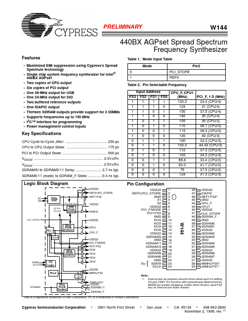
PRELIMINARY440BX AGPset Spread SpectrumFrequency SynthesizerW144Features•Maximized EMI suppression using Cypress’s Spread Spectrum technology•Single chip system frequency synthesizer for Intel ® 440BX AGPset•Two copies of CPU output •Six copies of PCI output •One 48-MHz output for USB •One 24-MHz output for SIO•Two buffered reference outputs •One IOAPIC output•Thirteen SDRAM outputs provide support for 3 DIMMs •Supports frequencies up to 150 MHz •I 2C™ interface for programming •Power management control inputsKey SpecificationsCPU Cycle-to-Cycle Jitter: .........................................250 ps CPU to CPU Output Skew: ........................................175 ps PCI to PCI Output Skew:............................................500 ps V DDQ3:....................................................................3.3V±5%V DDQ2:....................................................................2.5V±5%SDRAMIN to SDRAM0:11 Delay:..........................3.7 ns typ.SDRAM0:11 (leads) to SDRAM_F Skew:..............0.4 ns typ.Table 1.Mode Input TableModePin20PCI_STOP#1REF0Table 2.Pin Selectable FrequencyInput Address CPU_F, CPU1 (MHz)PCI_F, 1:5 (MHz)FS3FS2FS1FS01111133.333.3 (CPU/4)111012431 (CPU/4)110115037.5 (CPU/4)110014035 (CPU/4)101110535(CPU/3)101011036.7 (CPU/3)100111538.3 (CPU/3)100012040 (CPU/3)011110033.3 (CPU/3)0110133.344.43 (CPU/3)010111237.3 (CPU/3)010010334.3 (CPU/3)001166.833.4 (CPU/2)001083.341.7 (CPU/2)00017537.5 (CPU/2)000012441.3 (CPU/3)Intel is a registered trademark of Intel Corporation. I 2C is a trademark of Philips Corporation.Logic Block DiagramVDDQ3REF0/(PCI_STOP#)VDDQ2CPU1PCI_F/MODE XTAL PLL Ref FreqPLL 1X2X1REF1/FS2VDDQ3Stop Clock ControlStop Clock ControlPCI2PCI3PCI448MHz/FS024MHz/FS1PLL2÷2,3,4OSCVDDQ2CLK_STOP#VDDQ3IOAPIC PCI5I 2C SDA TA Logic SCLKI/O Pin ControlSDRAM0:11SDRAMIN12VDDQ3PCI1/FS3Stop Clock ControlStop Clock ControlCPU_F ÷2SDRAM_FPin ConfigurationVDDQ3REF0/(PCI_STOP#)GND X1X2VDDQ3PCI_F/MODEPCI1/FS3GND PCI2PCI3PCI4PCI5VDDQ3SDRAMINGND SDRAM11SDRAM10VDDQ3SDRAM9SDRAM8GNDSDA TA SCLKW144VDDQ2IOAPIC REF1/FS2*GND CPU_F CPU1VDDQ2CLK_STOP#SDRAM_F GND SDRAM0SDRAM1VDDQ3SDRAM2SDRAM3GND SDRAM4SDRAM5VDDQ3SDRAM6SDRAM7VDDQ348MHz/FS0*24MHz/FS1*484746454443424140393837363534333231302928272625123456789101112131415161718192021222324I 2C{Note:1.Internal pull-up resistors should not be relied upon for settingI/O pins HGH. Pin function with parentheses determined by MODE pin resistor strapping. Unlike other I/O pins, input FS3 has an internal pull down resistor.元器件交易网Pin DefinitionsPin Name Pin No.PinType Pin DescriptionCPU_F44O Free-running CPU Clock: Output voltage swing is controlled by the voltage applied toVDDQ2. See T ables 2 and 6 f or detailed frequency information.CPU143O CPU Clock Output 1: This CPU clock output is controlled by the CLK_STOP# controlpin. Output voltage swing is controlled by voltage applied to VDDQ2.PCI2:510, 11, 12,13O PCI Clock Outputs 2 through 5: These four PCI clock outputs are controlled by the PCI_STOP# control pin. Output voltage swing is controlled by voltage applied to VDDQ3.PCI1/FS38I/O Fixed PCI Clock Output: As an output. frequency is set by the FS0:3 inputs or throughserial input interface, see Tables 2 and 6. This output is affected by the PCI_STOP# input.When an input, latches data selecting the frequency of the CPU and PCI outputs.PCI_F/MODE7I/O Fixed PCI Clock Output: As an output, frequency is set by the FS0:3 inputs or throughserial input interface, see T ables 2 and 6. This output is not affected by the PCI_STOP#input. When an input, sets function of pin 2.CLK_STOP#41I CLK_STOP# input: When brought LOW, affected clock outputs are stopped LOW aftercompleting a full clock cycle (2–3 CPU clock latency). When brought HIGH, affected clockoutputs start, beginning with a full clock cycle (2–3 CPU clock latency).IOAPIC47O IOAPIC Clock Output: Provides 14.318-MHz fixed frequency. The output voltage swingis controlled by VDDQ2. This output is disabled when CLK_STOP# is set LOW.48MHz/FS026I/O48-MHz Output: 48 MHz is provided in normal operation. In standard systems, this outputcan be used as the reference for the Universal Serial Bus. Upon power-up FS0 input willbe latched, which will set clock frequencies as described in T able 2.24MHz/FS125I/O24-MHz Output:24 MHz is provided in normal operation. In standard systems, this outputcan be used as the clock input for a Super I/O chip. Upon power-up FS1 input will belatched, which will set clock frequencies as described in T able 2.REF1/FS246I/O I/O Dual-Function REF0 and FS2 pin: Upon power-up, FS2 input will be latched, whichwill set clock frequencies as described in Table 2. When an output, this pin provides afixed clock signal equal in frequency to the reference signal provided at the X1/X2 pins.REF0/(PCI_STOP#)2I/O Fixed 14.318-MHz Output 0 or PCI_STOP# Pin: Function determined by MODE pin.The PCI_STOP# input enables the PCI 1:5 outputs when HIGH and causes them toremain at logic 0 when LOW. The PCI_STOP signal is latched on the rising edge of PCI_F.Its effects take place on the next PCI_F clock cycle. When an output, this pin provides afixed clock signal equal in frequency to the reference signal provided at the X1/X2 pins.SDRAMIN15I Buffered Input Pin: The signal provided to this input pin is buffered to 13 outputs(SDRAM0:11, SDRAM_F).SDRAM0:1138, 37, 35,34, 32, 31,29, 28, 21,20, 18, 17O Buffered Outputs: These twelve dedicated outputs provide copies of the signal provided at the SDRAMIN input. The swing is set by VDDQ3, and they are deactivated whenCLK_STOP# input is set LOW.SDRAM_F40O Free-running Buffered Output: This dedicated output provides a copy of the SDRAMINinput which is not affected by the CLK_STOP# inputSCLK24I Clock pin for I2C CircuitrySDA TA23I/O Data pin for I2C CircuitryX14I Crystal Connection or External Reference Frequency Input: This pin has dual func-tions. It can be used as an external 14.318-MHz crystal connection or as an externalreference frequency input.X25I Crystal Connection:An input connection for an external 14.318-MHz crystal. If using anexternal reference, this pin must be left unconnected.VDDQ31, 6, 14,19, 27, 30,36P Power Connection: Power supply for core logic, PLL circuitry, SDRAM outputs, PCI outputs, reference outputs, 48-MHz output, and 24-MHz output. Connect to 3.3V supply.VDDQ242, 48P Power Connection: Power supply for IOAPIC, CPU_F, and CPU1 output buffers. Connectto 2.5V or 3.3V.GND3, 9, 16,22, 33, 39,45G Ground Connections: Connect all ground pins to the common system ground plane.OverviewThe W144 was developed as a single-chip device to meet the clocking needs of the Intel 440BX AGPset. In addition to the typical outputs provided by standard 100-MHz 440BX FTGs,the W144 adds a thirteen output buffer, supporting SDRAM DIMM modules in conjunction with the chipset.Cypress ’s proprietary spread spectrum frequency synthesis technique is a feature of the CPU and PCI outputs. When en-abled, this feature reduces the peak EMI measurements of not only the output signals and their harmonics, but also of any other clock signals that are properly synchronized to them.Functional DescriptionI/O Pin OperationPins 7, 8, 25, 26, and 46 are dual-purpose l/O pins. Upon pow-er-up these pins act as logic inputs, allowing the determination of assigned device functions. A short time after power-up, the logic state of each pin is latched and the pins become clock outputs. This feature reduces device pin count by combining clock outputs with input select pins.An external 10-k Ω “strapping ” resistor is connected between the l/O pin and ground or V DD . Connection to ground sets a latch to “0,” connection to V DD sets a latch to “1.” Figure 1 and Figure 2 show two suggested methods for strapping resistor connections.Upon W144 power up, the first 2 ms of operation is used for input logic selection. During this period, the five I/O pins (7, 8,25, 26, 46) are three-stated, allowing the output strapping re-sistor on the l/O pins to pull the pin and their associated ca-pacitive clock load to either a logic HIGH or LOW state. At the end of the 2ms period, the established logic “0” or “1” condition of the l/O pin is latched. Next the output buffer is enabled con-verting the l/O pins into operating clock outputs. The 2-ms tim-er starts when VDD reaches 2.0V . The input bits can only be reset by turning VDD off and then back on again.It should be noted that the strapping resistors have no signifi-cant effect on clock output signal integrity. The drive imped-ance of clock outputs are <40Ω (nominal) which is minimally affected by the 10-k Ω strap to ground or V DD . As with the se-ries termination resistor, the output strapping resistor should be placed as close to the l/O pin as possible in order to keep the interconnecting trace short. The trace from the resistor to ground or V DD should be kept less than two inches in length to prevent system noise coupling during input logic sampling.When the clock outputs are enabled following the 2-ms input period, the specified output frequency is delivered on the pin,assuming that V DD has stabilized. If V DD has not yet reached full value, output frequency initially may be below target but will increase to target once V DD voltage has stabilized. In either case, a short output clock cycle may be produced from the CPU clock outputs when the outputs are enabled.Power-on Reset TimerOutput Three-stateData LatchHold QDW144V DDClock Load10 k ΩOutput Buffer(Load Option 1)10 k Ω(Load Option 0)Output LowOutput Strapping R esistor Series Term ination ResistorFigure 1.Input Logic Selection Through Resistor Load OptionPower-on Reset TimerOutput Three-stateData LatchHold QDW144V DDClock LoadR10 k ΩOutput BufferOutput LowOutput Strapping Resistor Series Termination Resistor Jumper OptionsResistor Value RFigure 2.Input Logic Selection Through Jumper OptionSpread Spectrum FeatureThe device generates a clock that is frequency modulated in order to increase the bandwidth that it occupies. By increasing the bandwidth of the fundamental and its harmonics, the am-plitudes of the radiated electromagnetic emissions are re-duced. This effect is depicted in Figure 3.As shown in Figure 3, a harmonic of a modulated clock has a much lower amplitude than that of an unmodulated signal. The reduction in amplitude is dependent on the harmonic number and the frequency deviation or spread. The equation for the reduction isdB = 6.5 + 9*log10(P) + 9*log10(F)Where P is the percentage of deviation and F is the frequency in MHz where the reduction is measured.The output clock is modulated with a waveform depicted in Figure 4. This waveform, as discussed in “Spread Spectrum Clock Generation for the Reduction of Radiated Emissions ” by Bush, Fessler, and Hardin produces the maximum reduction in the amplitude of radiated electromagnetic emissions. The deviation selected for this chip is specified in Table 7. Figure 4details the Cypress spreading pattern. Cypress does offer op-tions with more spread and greater EMI reduction. Contact your local Sales representative for details on these devices.Spread Spectrum clocking is activated or deactivated by se-lecting the appropriate values for bits 1–0 in data byte 0 of the I 2C data stream. Refer to Table 7 for more details.Figure 3.Clock Harmonic with and without SSCGModulation Frequency Domain RepresentationSSFTGTypical ClockFrequency Span (M Hz)--SS%+SS%A m p l i t u d e (dB )5dB/divMAX (+0.5%)MIN (–0.5%)10%20%30%40%50%60%70%80%90%100%10%20%30%40%50%60%70%80%90%100%F R E Q U E N C YFigure 4.Typical Modulation ProfileSerial Data InterfaceThe W144 features a two-pin, serial data interface that can be used to configure internal register settings that control partic-ular device functions. Upon power-up, the W144 initializes with default register settings, therefore the use of this serial data interface is optional. The serial interface is write-only (to the clock chip) and is the dedicated function of device pins SDAT A and SCLOCK. In motherboard applications, SDA TA and SCLOCK are typically driven by two logic outputs of the chipset. Clock device register changes are normally made upon system initialization, if any are required. The interface can also be used during system operation for power manage-ment functions. T able 3 summarizes the control functions of the serial data interface. OperationData is written to the W144 in eleven bytes of eight bits each.Bytes are written in the order shown in T able 4.Table 3.Serial Data Interface Control Functions SummaryControl Function DescriptionCommon ApplicationClock Output DisableAny individual clock output(s) can be disabled. Disabled outputs are actively held LOW.Unused outputs are disabled to reduce EMI and system power. Examples are clock outputs to unused PCI slots.CPU Clock Frequency SelectionProvides CPU/PCI frequency selections through software. Frequency is changed in a smooth and controlled fashion.For alternate microprocessors and power management options. Smooth frequency transition allows CPU frequency change under normal system operation.Spread Spectrum EnablingEnables or disables spread spectrum clocking.For EMI reduction.Output Three-state Puts clock output into a high-impedance state.Production PCB testing.(Reserved)Reserved function for future device revision or production device testing.No user application. Register bit must be written as 0.Table 4.Byte Writing Sequence Byte SequenceByte Name Bit Sequence Byte Description1Slave Address11010010Commands the W144 to accept the bits in Data Bytes 0–6 for internal register configuration. Since other devices may exist on the same com-mon serial data bus, it is necessary to have a specific slave address for each potential receiver. The slave receiver address for the W144 is 11010010. Register setting will not be made if the Slave Address is not correct (or is for an alternate slave receiver).2Command Code Don ’t CareUnused by the W144, therefore bit values are ignored (“don ’t care ”). This byte must be included in the data write sequence to maintain proper byte allocation. The Command Code Byte is part of the standard serial communication protocol and may be used when writing to anoth-er addressed slave receiver on the serial data bus.3Byte Count Don ’t CareUnused by the W144, therefore bit values are ignored (“don ’t care ”). This byte must be included in the data write sequence to maintain proper byte allocation. The Byte Count Byte is part of the standard serial communication protocol and may be used when writing to anoth-er addressed slave receiver on the serial data bus.4Data Byte 0Refer to Table 5The data bits in Data Bytes 0–7 set internal W144 registers that control device operation. The data bits are only accepted when the Address Byte bit sequence is 11010010, as noted above. For description of bit control functions, refer to T able 5, Data Byte Serial Configuration Map.5Data Byte 16Data Byte 27Data Byte 38Data Byte 49Data Byte 510Data Byte 611Data Byte 7Writing Data BytesEach bit in Data Bytes 0–7 controls a particular device function except for the “reserved” bits, which must be written as a logic 0. Bits are written MSB (most significant bit) first, which is bit7. T able 5 gives the bit formats for registers located in Data Bytes 0–7. Table 6 details additional frequency selections that are avail-able through the serial data interface.Table 7 details the select functions for Byte 0, bits 1 and 0.Table 5.Data Bytes 0-7 Serial Configuration MapBit(s)Affected PinControl FunctionBit ControlDefault Pin No.Pin Name01Data Byte 07----(Reserved)----0 6----SEL_2See T able 60 5----SEL_1See T able 60 4----SEL_0See T able 60 3----Hardware/Software Frequency Select Hardware Software0 2----SEL_3See T able 60 1–0----Bit1Bit 0Function (See T able 7 for function details)00Normal Operation01(Reserved)10Spread Spectrum On11All Outputs Three-stated00Data Byte 17----(Reserved)----0 6----(Reserved)----0 5----(Reserved)----0 4----(Reserved)----0 340SDRAM_F Clock Output Disable Low Active1 2----(Reserved)----0 143CPU1Clock Output Disable Low Active1 044CPU_F Clock Output Disable Low Active1 Data Byte 27----(Reserved)----0 67PCI_F Clock Output Disable Low Active1 5----(Reserved)----0 413PCI5Clock Output Disable Low Active1 312PCI4Clock Output Disable Low Active1 211PCI3Clock Output Disable Low Active1 110PCI2Clock Output Disable Low Active1 08PCI1Clock Output Disable Low Active1 Data Byte 37----(Reserved)----0 6----(Reserved)----0 52648MHz Clock Output Disable Low Active1 42524MHz Clock Output Disable Low Active1 3----(Reserved)----0 221, 20,18, 17SDRAM8:11Clock Output Disable Low Active1132, 31, 29, 28SDRAM4:7Clock Output Disable Low Active 1038, 37, 35, 34SDRAM0:3Clock Output DisableLowActive1Data Byte 47----(Reserved)----06----(Reserved)----05----(Reserved)----04----(Reserved)----03----(Reserved)----02----(Reserved)----01----(Reserved)----00----(Reserved)----0Data Byte 57----(Reserved)----06----(Reserved)----05----(Reserved)----0447IOAPIC Clock Output Disable Low Active 13----(Reserved)----02----(Reserved)----0146REF1Clock Output Disable Low Active 102REF0Clock Output DisableLowActive1Data Byte 67----(Reserved)----06----(Reserved)----05----(Reserved)----04----(Reserved)----03----(Reserved)----02----(Reserved)----01----(Reserved)----00----(Reserved)----0Data Byte 77----(Reserved)----06----(Reserved)----05----(Reserved)----04----(Reserved)----03----(Reserved)----02----(Reserved)----01----(Reserved)----00----(Reserved)----0Table 5.Data Bytes 0-7 Serial Configuration Map (continued)Bit(s)Affected PinControl FunctionBit ControlDefault Pin No.Pin Name 01Table 6.Additional Frequency Selections through Serial Data Interface Data BytesInput Conditions Output FrequencyData Byte 0, Bit 3 = 1CPU, SDRAM Clocks(MHz)PCI Clocks (MHz)Bit 2 SEL_3Bit 6SEL_2Bit 5SEL_1Bit 4SEL_01111133.333.3 (CPU/4) 111012431 (CPU/4) 110115037.5 (CPU/4) 110014035 (CPU/4) 101110535 (CPU/3) 101011036.7 (CPU/3) 100111539.3 (CPU/3) 100012040 (CPU/3) 011110033.3 (CPU/3) 011013344.3 (CPU/3) 010111237.3 (CPU/3) 010010334.3 (CPU/3) 001166.833.4 (CPU/2) 001083.341.7 (CPU/2) 00017537.5 (CPU/2) 000012441.3 (CPU/3)Table 7.Select Function for Data Byte 0, Bits 0:1Function Input Conditions Output ConditionsData Byte 0CPU_F,CPU1PCI_F,PCI1:5REF0:1,IOAPIC48MHZ24MHZ Bit 1Bit 0Normal Operation00Note 1Note 114.318 MHz48 MHz24 MHz Spread Spectrum10±0.5%±0.5%14.318 MHz48 MHz24 MHz Three-state11Hi-Z Hi-Z Hi-Z Hi-Z Hi-Z Note:2.CPU and PCI frequency selections are listed in T able 2 and T able 6.Absolute Maximum RatingsStresses greater than those listed in this table may cause per-manent damage to the device. These represent a stress rating only. Operation of the device at these or any other conditions above those specified in the operating sections of this specifi-cation is not implied. Maximum conditions for extended peri-ods may affect reliabilityParameter Description Rating UnitV DD, V IN Voltage on any pin with respect to GND–0.5 to +7.0VT STG Storage T emperature–65 to +150°CT B Ambient T emperature under Bias–55 to +125°CT A Operating Temperature0 to +70°CESD PROT Input ESD Protection 2 (min)kVDC Electrical Characteristics:T A = 0°C to +70°C; V DDQ3 = 3.3V±5%; V DDQ2 = 2.5V±5%Parameter Description Test Condition Min.Typ.Max.Unit Supply CurrentI DD 3.3V Supply Current CPU_F, CPU1 = 100 MHzOutputs Loaded[3]260mAI DD 2.5V Supply Current CPU_F, CPU1 = 100 MHzOutputs Loaded[3]25mA Logic InputsV IL Input Low Voltage GND –0.30.8VV IH Input High Voltage 2.0V DDQ3 +0.3V I IL Input Low Current[4]–25µA I IH Input High Current[4]10µA I IL Input Low Current (SEL100/66#) –5µA I IH Input High Current (SEL100/66#)+5µA Clock OutputsV OL Output Low Voltage I OL = 1 mA50mV V OH Output High Voltage I OH = 1 mA 3.1V V OH Output High Voltage CPU_F,1,IOAPICI OH = –1 mA 2.2V I OL Output Low Current CPU_F, CPU1V OL = 1.25V275797mAPCI_F, PCI1:5V OL = 1.5V20.553139mAIOAPIC V OL = 1.25V4085140mAREF0:1V OL = 1.5V253776mA48MHz V OL = 1.5V253776mA24MHz V OL = 1.5V253776mA I OH Output High Current CPU_F, CPU1V OH = 1.25V255597mAPCI_F, PCI1:5V OH = 1.5V3155139mAIOAPIC V OH = 1.25V4087155mAREF0:1V OH = 1.5V274494mA48MHz V OH = 1.5V274494mA24MHz V OH = 1.5V253776mAAC Electrical CharacteristicsT A = 0°C to +70°C; V DDQ3 = 3.3V±5%; V DDQ2 = 2.5V±5%; f XTL = 14.31818 MHzAC clock parameters are tested and guaranteed over stated operating conditions using the stated lump capacitive load at the clock output; Spread Spectrum clocking is disabled.Crystal Oscillator V TH X1 Input threshold Voltage [5]V DDQ3 = 3.3V1.65V C LOAD Load Capacitance, Imposed on External Crystal [6]14pF C IN,X1X1 Input Capacitance [7]Pin X2 unconnected 28pF Pin Capacitance/InductanceC IN Input Pin Capacitance Except X1 and X25pF C OUT Output Pin Capacitance 6pF L INInput Pin Inductance7nHNotes:3.All clock outputs loaded with 6" 60Ω traces with 22-pF capacitors.4.W144 logic inputs (except FS3) have internal pull-up devices (pull-ups not full CMOS level). Logic input FS3 has an internal pull-down device.5.X1 input threshold voltage (typical) is V DDQ3/2.6.The W144 contains an internal crystal load capacitor between pin X1 and ground and another between pin X2 and ground. Total load placed on crystal is14pF; this includes typical stray capacitance of short PCB traces to crystal.7.X1 input capacitance is applicable when driving X1 with an external clock source (X2 is left unconnected).DC Electrical Characteristics: (continued)T A = 0°C to +70°C; V DDQ3 = 3.3V±5%; V DDQ2 = 2.5V±5%Parameter DescriptionTest ConditionMin.Typ.Max.Unit CPU Clock Outputs, CPU_F, CPU1 (Lump Capacitance Test Load = 20 pF)Parameter Description Test Condition/Comments CPU = 66.6 MHzCPU = 100 MHz UnitMin.Typ.Max.Min.Typ.Max.t P Period Measured on rising edge at 1.251515.51010.5ns t H High Time Duration of clock cycle above 2.0V 5.6 3.3ns t L Low TimeDuration of clock cycle below 0.4V 5.3 3.1ns t R Output Rise Edge Rate Measured from 0.4V to 2.0V1.54 1.54V/ns t F Output Fall Edge Rate Measured from2.0V to 0.4V1.54 1.54V/ns t D Duty CycleMeasured on rising and falling edge at 1.25V45554555%t JCJitter, Cycle-to-CycleMeasured on rising edge at 1.25V. Max-imum difference of cycle time between two adjacent cycles.200200pst SK Output Skew Measured on rising edge at 1.25V 250250ps f STFrequency Stabiliza-tion from Power-up (cold start)Assumes full supply voltage reached within 1 ms from power-up. Short cycles exist prior to frequency stabilization.33msZ oAC Output ImpedanceAverage value during switching transi-tion. Used for determining series termi-nation value.2020ΩSDRAM Clock Outputs, SDRAM, SDRAM0:11 (Lump Capacitance Test Load = 30 pF)Parameter Description Test Condition/CommentsCPU = 66.6 MHz CPU = 100 MHzUnit Min.Typ.Max.Min.Typ.Max.t P Period Measured on rising edge at 1.5V3030ns t H High Time Duration of clock cycle above 2.4V,at min. edge rate (1.5V/ns)5.6 3.3nst L Low Time Duration of clock cycle below 0.4V,at min. edge rate (1.5V/ns)5.3 3.1nst R Output Rise EdgeRateMeasured from 0.4V to 2.4V 1.54 1.54V/nst F Output Fall EdgeRateMeasured from 2.4V to 0.4V 1.54 1.54V/ns t PLH Prop Delay LH Input edge rate faster than 1V/ns1515ns t PHL Prop Delay HL Input edge rate faster than 1V/ns1515ns t D Duty Cycle Measured on rising and fallingedge at 1.5V,at min. sdge rate(1.5V/ns)45554555%t JC Jitter, Cycle-to-Cycle Measured on rising edge at 1.5V.Maximum difference of cycle timebetween two adjacent cycles.250250ps t SK Output Skew Measured on rising edge at 1.5V250250pst O CPU to PCI ClockSkew Covers all CPU/PCI outputs. Mea-sured on rising edge at 1.5V. CPUleads PCI output.1.54 1.54nsf ST FrequencyStabilization fromPower-up (cold start)Assumes full supply voltagereached within 1 ms from power-up. Short cycles exist prior to fre-quency stabilization.33msZ o AC OutputImpedance Average value during switchingtransition. Used for determiningseries termination value.3030ΩPCI Clock Outputs, PCI_F and PCI1:5 (Lump Capacitance Test Load = 30 pF)Parameter Description Test Condition/CommentsCPU = 66.6/100 MHzUnit Min.Typ.Max.t P Period Measured on rising edge at 1.5V30ns t H High Time Duration of clock cycle above 2.4V 12.0ns t L Low Time Duration of clock cycle below 0.4V12.0ns t R Output Rise Edge Rate Measured from 0.4V to 2.4V14V/ns t F Output Fall Edge Rate Measured from 2.4V to 0.4V 14V/ns t D Duty Cycle Measured on rising and falling edge at 1.5V4555% t JC Jitter, Cycle-to-Cycle Measured on rising edge at 1.5V. Maximumdifference of cycle time between two adja-cent cycles.250pst SK Output Skew Measured on rising edge at 1.5V500ps t O CPU to PCI Clock Skew Covers all CPU/PCI outputs. Measured onrising edge at 1.5V. CPU leads PCI output.1.5 4.0nsf ST Frequency Stabilizationfrom Power-up (cold start)Assumes full supply voltage reached within1ms from power-up. Short cycles exist pri-or to frequency stabilization.3.0msZ o AC Output Impedance Average value during switching transition.Used for determining series terminationvalue.30ΩIOAPIC Clock Output (Lump Capacitance Test Load = 20 pF)Parameter Description Test Condition/CommentsCPU = 66.6/100 MHzUnit Min.Typ.Max.f Frequency, Actual Frequency generated by crystal oscillator14.31818MHz t R Output Rise Edge Rate Measured from 0.4V to 2.0V14V/ns t F Output Fall Edge Rate Measured from 2.0V to 0.4V14V/ns t D Duty Cycle Measured on rising and falling edge at 1.25V4555%f ST Frequency Stabilizationfrom Power-up (cold start)Assumes full supply voltage reached within1ms from power-up. Short cycles exist priorto frequency stabilization.1.5msZ o AC Output Impedance Average value during switching transition.Used for determining series termination value.15ΩREF0:1 Clock Output (Lump Capacitance Test Load = 20 pF)Parameter Description Test Condition/Comments CPU = 66.6/100 MHzUnit Min.Typ.Max.f Frequency, Actual Frequency generated by crystal oscillator14.318MHz t R Output Rise Edge Rate Measured from 0.4V to 2.4V0.52V/ns t F Output Fall Edge Rate Measured from 2.4V to 0.4V0.52V/ns t D Duty Cycle Measured on rising and falling edge at 1.5V4555%f ST Frequency Stabilizationfrom Power-up (coldstart)Assumes full supply voltage reached within 1 ms frompower-up. Short cycles exist prior to frequency stabili-zation.3msZ o AC Output Impedance Average value during switching transition. Used for de-termining series termination value.40Ω。
Miwell-Combi XSL微波炉使用说明书
感谢您选择购买我们的产品。
您的设备满足高标准的要求,并且操作简便。
但仍请您抽出时间阅读本操作说明书。
这样您可以了解您的设备,并且在其最佳状态、无故障地使用该设备。
请您遵守安全提示。
更改文字、图片和数据均相应于本操作说明书排印时的设备当前技术水平。
保留因继续研发而更改的权利。
有效范围产品系列号(型号编码)与型号铭牌上的前几位相对应。
此操作说明书适用于:规格差异在文本中进行了描述。
可访问网址 下载彩色版操作说明书。
© V-ZUG Ltd, CH-6301 Zug, 20152目录1安全提示 61.1使用的符号 (6)1.2一般性安全提示 (6)1.3设备特有的安全提示 (7)1.4使用说明 (8)1.5配件 (10)2废弃处理 12 3首次使用 13 4设备说明 144.1结构 (14)4.2操作和显示元件 (14)4.3烤箱 (15)4.4配件 (16)4.5通风 (17)4.6安装 (18)5运行方式 195.1运行方式概览 (19)5.2常用设置 (19)5.3微波 (20)5.4CombiCrunch (22)5.5热空气 (23)5.6热空气组合运行 (23)5.7快速加热 (24)5.8烧烤 (24)5.9烧烤组合运行 (25)5.10热风循环烧烤 (26)5.11热风循环烧烤组合运行 (27)6操作 286.1选择和启动运行方式 (29)6.2更改微波功率/温度 (30)6.3更改运行方式 (30)6.4更改持续时间 (30)6.5定时器 (31)36.6中断 (32)6.7继续 (32)6.8取消运行 (32)6.9运行结束 (33)6.10关闭设备 (34)7AutomaticPlus 357.1概览 (35)7.2选择和启动自动程序 (38)8技巧和窍门 398.1对烹饪结果不满意 (39)8.2省电 (40)9用户设置 419.1选择用户设置 (41)9.2调整用户设置 (41)9.3语言 (41)9.4儿童安全锁 (42)9.5时钟功能 (42)9.6灯 (43)9.7叮响声 (43)9.8温度单位 (43)9.9时间格式 (43)9.10对比度 (44)9.11出厂设置 (44)10维护和保养 4510.1外部清洁 (45)10.2清洁设备门 (45)10.3清洁门密封件 (45)10.4清洁烤箱 (46)10.5清洁配件 (46)10.6更换卤素灯 (46)11自行排除故障 4711.1发生以下情况时应采取的措施 (47)11.2断电后 (48)12配件和备件 49 413技术数据 5113.1温度测量 (51)13.2待机节能程序 (51)14索引 52 15服务 & 技术支持 5551 安全提示1.1 使用的符号标记所有对安全来说非常重要的指令。
LT1244资料

BLOCK DIAGRA
RT/CT 4
COMP 1
FB 2
–
2.5V
+
ISENSE 3
OSCILLATOR
5.6V 1mA
2R
1V
–
R
+
5V REF MAIN BIAS
REFERENCE ENABLE REFERENCE PULL-DOWN
UV LOCKOUT
OUTPUT PULL-DOWN
T
S R
CONDITIONS
IO = 1mA, TJ = 25°C
12V < VCC < 25V
q
1mA < IVREF < 20mA
q
Line, Load, Temp
q
10Hz < F < 10kHz, TJ = 25°C TA = 125°C, 1000 Hrs.
q
RT = 10k, CT = 3.3nF, TJ = 25°C RT = 13.0k, CT = 500pF, TJ = 25°C 12V < VCC < 25V, TJ = 25°C TMIN < TJ < TMAX TJ = 25°C (Pin 4) VOSC (Pin 4) = 2V, TJ = 25°C
Output High Level
Rise Time Fall Time Output Clamp Voltage Undervoltage Lockout Start-Up Threshold
LT1241 LT1242/LT1244 LT1243/LT1245 Minimum Operating Voltage LT1241/LT1243/LT1245 LT1242/LT1244 Hysteresis LT1241 LT1242/LT1244 LT1243/LT1245 PWM Maximum Duty Cycle LT1241/LT1244/LT1245 LT1242/LT1243 Minimum Duty Cycle Total Device Start-Up Current Operating Current
2SA1244中文资料
V
―
60
― MHz
― 170 ―
pF
Turn-on time Switching time Storage time
ton
OUTPUT ―
0.1
―
20 μs INPUT IB2
IB1 10 Ω
tstg
IB2
IB1
―
1.0
―
μs
VCC = −30 V
Fall time
tf
−IB1 = IB2 = 0.15 A,
50 × 50 × 0.8 mm (3) No heat sink
16
12
8
4 (2) (3)
0 0 20 40 60 80 100 120 140 160
Ambient temperature Ta (°C)
Collector current IC (A)
4
2006-11-09
2SA1244
RESTRICTIONS ON PRODUCT USE
−20 −40
−80
−150
−200
−0.6
−100
−300 −0.4
−400
−500 −0.2
0
0
−1
−2
−3
−4
−5
−6
−7
Collector current IC (A)
Collector-emitter voltage VCE (V)
DC current gain hFE
1000 500 300
DUTY CYCLE ≤ 1%
Note: hFE (1) classification O: 70 to 140, Y: 120 to 240
微尔赛米集团2013年产品说明书
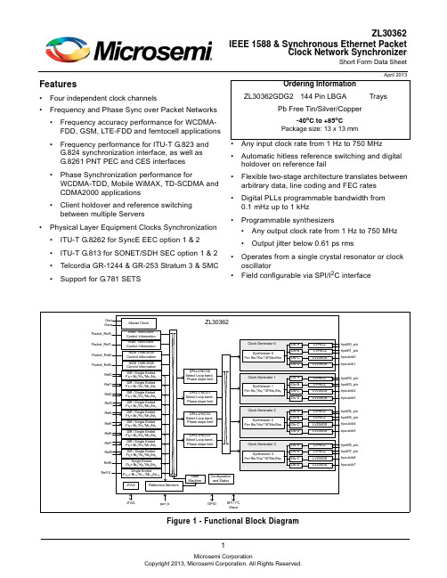
1Features•Four independent clock channels•Frequency and Phase Sync over Packet Networks •Frequency accuracy performance for WCDMA-FDD, GSM, LTE-FDD and femtocell applications •Frequency performance for ITU-T G.823 and G.824 synchronization interface, as well as G.8261 PNT PEC and CES interfaces•Phase Synchronization performance forWCDMA-TDD, Mobile WiMAX, TD-SCDMA and CDMA2000 applications•Client holdover and reference switching between multiple Servers•Physical Layer Equipment Clocks Synchronization •ITU-T G.8262 for SyncE EEC option 1 & 2•ITU-T G.813 for SONET/SDH SEC option 1 & 2•Telcordia GR-1244 & GR-253 Stratum 3 & SMC •Support for G.781 SETS•Any input clock rate from 1Hz to 750MHz •Automatic hitless reference switching and digital holdover on reference fail•Flexible two-stage architecture translates between arbitrary data, line coding and FEC rates •Digital PLLs programmable bandwidth from 0.1mHz up to 1kHz•Programmable synthesizers•Any output clock rate from 1 Hz to 750 MHz •Output jitter below 0.61 ps rms•Operates from a single crystal resonator or clock oscillator•Field configurable via SPI/I 2C interfaceApril 2013Figure 1 - Functional Block DiagramZL30362IEEE 1588 & Synchronous Ethernet PacketClock Network SynchronizerShort Form Data SheetOrdering InformationZL30362GDG2144 Pin LBGATraysPb Free Tin/Silver/Copper-40o C to +85o CPackage size: 13 x 13 mmDetailed FeaturesGeneral•Four independent clock channels•Operates from a single crystal resonator or clock oscillator•Configurable its SPI/I2C interfaceTime Synchronization Algorithm•External algorithm controls software digital PLL to adjust frequency & phase alignment•Frequency, Phase and Time Synchronization over IP, MPLS and Ethernet Packet Networks•Frequency accuracy performance for WCDMA-FDD, GSM, LTE-FDD and femtocell applications, with target performance less than ± 15 ppb.•Frequency performance for ITU-T G.823 and G.824 synchronization interface, as well as G.8261 PNT EEC, PNT PEC and CES interface specifications.•Phase Synchronization performance for WCDMA-TDD, Mobile WiMAX, TD-SCDMA and CDMA2000 applications with target performance less than ± 1 s phase alignment.•Time Synchronization for UTC-traceability and GPS replacement.•Client reference switching between multiple Servers•Client holdover when Server packet connectivity is lostElectrical Clock Inputs•Nine input references configurable as single ended or differential and two single ended input references •Synchronize to any clock rate from 1 Hz to 750 MHz on differential inputs•Synchronize to any clock rate from 1 Hz to 177.75 MHz on singled-ended inputs•Any input reference can be fed with sync (frame pulse) or clock.•Synchronize to sync pulse and sync pulse/clock pair.•Flexible input reference monitoring automatically disqualifies references based on frequency and phase irregularities•LOS•Single cycle monitor•Precise frequency monitor•Coarse frequency monitor•Guard soak timer•Per input clock delay compensationElectrical Clock Engine•Digital PLLs filter jitter from 0.1 mHz up to 1 kHz•Flexible two-stage architecture translates between arbitrary data rates, line coding rates and FEC rates •Internal state machine automatically controls mode of operation (free-run, locked, holdover)•Automatic hitless reference switching and digital holdover on reference fail•Physical-to-physical reference switching•Physical-to-packet reference switching•Packet-to-physical reference switching•Packet-to-packet reference switching•Support for wide variety of Equipment Clock specifications•SyncE•ITU-T G.8262 option 1 EEC (Europe/China)•ITU-T G.8262 option 2 (USA)•SONET/SDH•ITU-T G.813 option 1 SEC (Europe/China)•ITU-T G.813 option 2 (USA)•ANSI T1.105/Telcordia GR-253 Stratum 3 for SONET•Telcordia GR-253 SMC•PDH•ITU-T G.812 Type I SSU•ITU-T G.812 Type III, ANSI T1.101/Telcordia GR-1244 Stratum 3E, including phase build out•ANSI T1.101/Telcordia GR-1244 Stratum 3•ANSI T1.101/Telcordia GR-1244 Stratum 4E/4•Selectable phase slope limiting•Holdover better than 1 ppb (when using < 0.1 Hz filter)•Supports ITU-T G.823, G.824 and G.8261 for 2048kbit/s and 1544kbit/s interfaces•Supports G.781 SETSElectrical Clock Generation•Four programmable synthesizers•Eight LVPECL outputs•Two LVPECL outputs per synthesizer•Generate any clock rate from 1 Hz to 750 MHz•Maximum jitter below 0.61 ps RMS•Meets OC-192, STM-64, 1 GbE & 10 GbE interface jitter requirements•Eight LVCMOS outputs•Two LVCMOS outputs per synthesizer•Generate any clock rate from 1 Hz to 177.75 MHz•Maximum jitter below 1 ps rms•Programmable output advancement/delay to accommodate trace delays or compensate for system routing paths•Outputs may be disabled to save powerAPI Software•Interfaces to 1588-capable PHY and switches with integrated timestamping•Abstraction layer for independence from OS and CPU, from embedded SoC to home-grown•Fits into centralized, highly integrated pizza box architectures as well as distributed architectures with multiple line cards and timing cardsApplications•ITU-T G.8262 System Timing Cards which support 1GbE and 10GbE interfaces•Telcordia GR-253 Carrier Grade SONET/SDH Stratum 3 System Timing Cards•System Timing Cards which supports ITU-T G.781 SETS (SDH Equipment Timing Source)•Integrated basestation reference clock for air interface for GSM, WCDMA, LTE and WiMAX macro, micro or femtocells•Mobile Backhaul NID, edge router or access aggregation node•EPON/GE-PON & GPON OLT•EPON/GE-PON & GPON ONU/OLT•DSLAM and RT-DSLAM•10Gigabit line cards•Synchronous Ethernet, 10GBASE-R and 10GBASE-W•SONET/SDH, Fibre Channel, XAUIInformation relating to products and services furnished herein by Microsemi Corporation or its subsidiaries (collectively “Microsemi”) is believed to be reliable. However, Microsemi assumes no liability for errors that may appear in this publication, or for liability otherwise arising from the application or use of any suchinformation, product or service or for any infringement of patents or other intellectual property rights owned by third parties which may result from such application or use. Neither the supply of such information or purchase of product or service conveys any license, either express or implied, under patents or other intellectual property rights owned by Microsemi or licensed from third parties by Microsemi, whatsoever. Purchasers of products are also hereby notified that the use of product in certain ways or in combination with Microsemi, or non-Microsemi furnished goods or services may infringe patents or other intellectual property rights owned by Microsemi.This publication is issued to provide information only and (unless agreed by Microsemi in writing) may not be used, applied or reproduced for any purpose nor form part of any order or contract nor to be regarded as a representation relating to the products or services concerned. The products, their specifications, services and other information appearing in this publication are subject to change by Microsemi without notice. No warranty or guarantee express or implied is made regarding the capability, performance or suitability of any product or service. Information concerning possible methods of use is provided as a guide only and does not constitute any guarantee that such methods of use will be satisfactory in a specific piece of equipment. It is the user’s responsibility to fully determine the performance and suitability of any equipment using such information and to ensure that any publication or data used is up to date and has not been superseded.Manufacturing does not necessarily include testing of all functions or parameters. These products are not suitable for use in any medical and other products whose failure to perform may result in significant injury or death to the user. All products and materials are sold and services provided subject to Microsemi’s conditions of sale which are available on request.Purchase of Microsemi’s I 2C components conveys a license under the Philips I 2C Patent rights to use these components in an I 2C System, provided that the system conforms to the I 2C Standard Specification as defined by Philips.Microsemi, ZL, and combinations thereof, VoiceEdge, VoicePort, SLAC, ISLIC, ISLAC and VoicePath are trademarks of Microsemi Corporation.TECHNICAL DOCUMENTATION - NOT FOR RESALEFor more information about all Microsemi productsvisit our Web Site at/timing-and-synchronization。
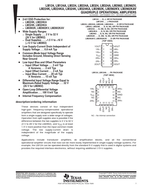
LM124DR中文资料
元器件交易网元器件交易网IMPORTANT NOTICETexas Instruments Incorporated and its subsidiaries (TI) reserve the right to make corrections, modifications,enhancements, improvements, and other changes to its products and services at any time and to discontinueany product or service without notice. Customers should obtain the latest relevant information before placingorders and should verify that such information is current and complete. All products are sold subject to TI’s termsand conditions of sale supplied at the time of order acknowledgment.TI warrants performance of its hardware products to the specifications applicable at the time of sale inaccordance with TI’s standard warranty. T esting and other quality control techniques are used to the extent TIdeems necessary to support this warranty. Except where mandated by government requirements, testing of allparameters of each product is not necessarily performed.TI assumes no liability for applications assistance or customer product design. Customers are responsible fortheir products and applications using TI components. T o minimize the risks associated with customer productsand applications, customers should provide adequate design and operating safeguards.TI does not warrant or represent that any license, either express or implied, is granted under any TI patent right,copyright, mask work right, or other TI intellectual property right relating to any combination, machine, or processin which TI products or services are used. Information published by TI regarding third-party products or servicesdoes not constitute a license from TI to use such products or services or a warranty or endorsement thereof.Use of such information may require a license from a third party under the patents or other intellectual propertyof the third party, or a license from TI under the patents or other intellectual property of TI.Reproduction of information in TI data books or data sheets is permissible only if reproduction is withoutalteration and is accompanied by all associated warranties, conditions, limitations, and notices. Reproductionof this information with alteration is an unfair and deceptive business practice. TI is not responsible or liable forsuch altered documentation.Resale of TI products or services with statements different from or beyond the parameters stated by TI for thatproduct or service voids all express and any implied warranties for the associated TI product or service andis an unfair and deceptive business practice. TI is not responsible or liable for any such statements.Following are URLs where you can obtain information on other Texas Instruments products and applicationsolutions:Products ApplicationsAmplifiers Audio /audioData Converters Automotive /automotiveDSP Broadband /broadbandInterface Digital Control /digitalcontrolLogic Military /militaryPower Mgmt Optical Networking /opticalnetworkMicrocontrollers Security /securityTelephony /telephonyVideo & Imaging /videoWireless /wirelessMailing Address:Texas InstrumentsPost Office Box 655303 Dallas, Texas 75265Copyright 2005, Texas Instruments Incorporated。
AN-1244中文资料
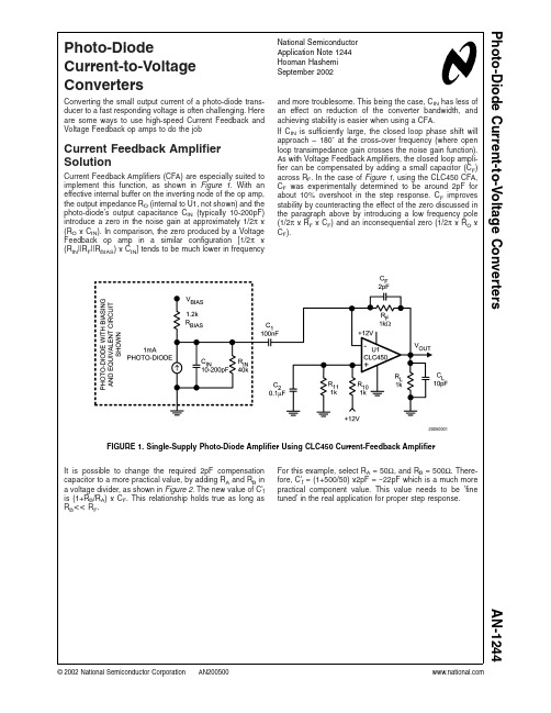
Photo-DiodeCurrent-to-Voltage ConvertersConverting the small output current of a photo-diode trans-ducer to a fast responding voltage is often challenging.Here are some ways to use high-speed Current Feedback and Voltage Feedback op amps to do the jobCurrent Feedback Amplifier SolutionCurrent Feedback Amplifiers (CFA)are especially suited to implement this function,as shown in Figure 1.With an effective internal buffer on the inverting node of the op amp,the output impedance R O (internal to U1,not shown)and the photo-diode’s output capacitance C IN (typically 10-200pF)introduce a zero in the noise gain at approximately 1/2πx (R O x C IN ).In comparison,the zero produced by a Voltage Feedback op amp in a similar configuration [1/2πx (R IN ||R F ||R BIAS )x C IN ]tends to be much lower in frequencyand more troublesome.This being the case,C IN has less of an effect on reduction of the converter bandwidth,and achieving stability is easier when using a CFA.If C IN is sufficiently large,the closed loop phase shift will approach –180˚at the cross-over frequency (where open loop transimpedance gain crosses the noise gain function).As with Voltage Feedback Amplifiers,the closed loop ampli-fier can be compensated by adding a small capacitor (C F )across R F .In the case of Figure 1,using the CLC450CFA,C F was experimentally determined to be around 2pF for about 10%overshoot in the step response.C F improves stability by counteracting the effect of the zero discussed in the paragraph above by introducing a low frequency pole (1/2πx R F x C F )and an inconsequential zero (1/2πx R O x C F ).It is possible to change the required 2pF compensation capacitor to a more practical value,by adding R A and R B in a voltage divider,as shown in Figure 2.The new value of C'f is (1+R B /R A )x C F .This relationship holds true as long as R B <<R F .For this example,select R A =50Ω,and R B =500Ω.There-fore,C'f =(1+500/50)x2pF =~22pF which is a much more practical component value.This value needs to be ’fine tuned’in the real application for proper step response.20050001FIGURE 1.Single-Supply Photo-Diode Amplifier Using CLC450Current-Feedback AmplifierNational Semiconductor Application Note 1244Hooman Hashemi September 2002Photo-Diode Current-to-Voltage ConvertersAN-1244©2002National Semiconductor Corporation Current Feedback Amplifier Solution (Continued)Voltage Feedback Amplifier SolutionIt’s more difficult to design a good current-to-voltage con-verter using a Voltage Feedback Amplifier (VFA).As dis-cussed above,phase shift caused by photo-diode capaci-tance is often a source of instability.Furthermore,wide bandwidth usually comes at the expense of supply currents and higher supply voltage.However,the new LMH6642high-speed low-voltage VFA op amp has excellent perfor-mance in a transimpedance gain block,as shown in Figure 3.This device can operate down to 2.7V single supply and its −3dB BW (A V =+1)is more than 100MHz (with a supply current of only 2.7mA)!Because of the ’Dielectric Isolation’process this device is based on,the traditional supply volt-age vs.speed trade-off has been alleviated to a great extent allowing low power consumption and operation at lower supply voltages.In addition,the device has Rail-to-Rail out-put swing capability to maximize the output swing,and is capable of driving ±50mA into the load.With 5V single supply,the device common mode voltage is shifted to near half-supply using R 10-R 11as a voltage divider from V CC .The common-base transistor stage (Q1)isolates the photo-diode’s capacitance from the inverting terminal,allowing wider bandwidth and easing the compensation re-quired.Note that the collector of Q1does not have any voltage swing,so the Miller effect is minimized.The diode on the base of Q1is for temperature compensation of its bias point.Q1bias current was set to be large enough to handle the peak-to-peak photo-diode excitation,yet not too large as to shift the U1output too far from mid-supply.The overall circuit draws about 4.5mA from the +5V power supply and achieves about 35MHz of closed loop bandwidth @1V PP .Figure 4shows the output large signal step response.C F can be increased to reduce the overshoot,at the expense of bandwidth.20050002FIGURE 2.R A -R B Resistor Divider Allows Use ofPractical Value for C'f20050003FIGURE 3.Single-Supply Photo-Diode Amplifier Using LMH6642Voltage-Feedback Op AmpA N -1244 2Voltage Feedback Amplifier Solution(Continued)LIFE SUPPORT POLICYNATIONAL’S PRODUCTS ARE NOT AUTHORIZED FOR USE AS CRITICAL COMPONENTS IN LIFE SUPPORT DEVICES OR SYSTEMS WITHOUT THE EXPRESS WRITTEN APPROVAL OF THE PRESIDENT AND GENERAL COUNSEL OF NATIONAL SEMICONDUCTOR CORPORATION.As used herein:1.Life support devices or systems are devices orsystems which,(a)are intended for surgical implantinto the body,or(b)support or sustain life,andwhose failure to perform when properly used inaccordance with instructions for use provided in thelabeling,can be reasonably expected to result in asignificant injury to the user.2.A critical component is any component of a lifesupport device or system whose failure to performcan be reasonably expected to cause the failure ofthe life support device or system,or to affect itssafety or effectiveness.National SemiconductorCorporationAmericasEmail:support@National SemiconductorEuropeFax:+49(0)180-5308586Email:europe.support@Deutsch Tel:+49(0)6995086208English Tel:+44(0)8702402171Français Tel:+33(0)141918790National SemiconductorAsia Pacific CustomerResponse GroupTel:65-2544466Fax:65-2504466Email:ap.support@National SemiconductorJapan Ltd.Tel:81-3-5639-7560Fax:81-3-5639-7507 20050004FIGURE4.Output Step Response20ns/div,0.2V/divPhoto-DiodeCurrent-to-VoltageConvertersAN-1244 National does not assume any responsibility for use of any circuitry described,no circuit patent licenses are implied and National reserves the right at any time without notice to change said circuitry and specifications.。
GMW14124-2012中文版
汽车环境周期1范围注:在本标准中没有将取代适用的法律和法规。
注:在英语和本国语言之间的冲突时,以英文为准。
1.1目的。
此程序文件各种环境周期以及可以在测试之前或作为一个完整的测试进行老化条件。
本规范不包括用于测试或测试前预处理标准条件。
这些要求既可以在材料规格或在GMW3221找到。
1.2前言。
此程序文件已在有关材料规格的全球商定几个周期。
只有那些周期应选择创建GMW材料规格要求。
根据有关材料规格的周期全球公认的有:循环M,Q,R,S,T,U,V和W对于测试周期用途,见4.1.2。
1.3适用性。
请参阅表1的适用性。
注意:某些在本说明书中的测试周期的,最好用作质量控制测试,并且不意味着以验证势场的性能。
更多详情参见平台的材料工程师。
2参考注:除非另有规定,只有最新批准的标准都适用。
2.1外部标准/规范。
ISO9227VDA621-4152.2 GM标准/规范。
GMW3221GMW14444GMW15288GMW3286GMW147293资源3.1设施。
不适用。
3.2设备。
3.2.1机械对流烤箱能够保持从材料规范所要求的温度,以±3℃的公差。
3.2.2恒温恒湿箱能够保持从材料规格所需湿度的±3%的公差的。
3.2.3盐雾柜组成的雾室,盐溶液贮存器,适当地调节压缩空气的供给,一个或多个雾化喷嘴,试样支架,用于加热腔室和控制的必要手段的规定。
是可选的设置大小和盐雾机柜详细结构得到的条件符合该方法的要求。
合适的设备,在ISO 9227中描述。
3.2.4冷室或冷室与能够维持从材料规范要求的温度在±3℃的公差的端口孔。
3.2.5机架或夹具需要支持从垂直位置15和30度之间的试验样品以这样的方式,以防止试验样品或能够创建电偶的任何金属材料之间的接触。
3.2.6蒸汽高压灭菌能够维持所需的温度在±2℃,并能够承受高于大气压(即,2.5巴绝对)高达1.5巴(150千帕)的压力。
将高压釜必须能够在试验完成放空,以防止水过分起泡在打开腔室。
- 1、下载文档前请自行甄别文档内容的完整性,平台不提供额外的编辑、内容补充、找答案等附加服务。
- 2、"仅部分预览"的文档,不可在线预览部分如存在完整性等问题,可反馈申请退款(可完整预览的文档不适用该条件!)。
- 3、如文档侵犯您的权益,请联系客服反馈,我们会尽快为您处理(人工客服工作时间:9:00-18:30)。
Dual OutputSingle OutputBlock DiagramMIW1200-Series power modules are low-profiledc-dc converters that operate over input voltage ranges of 9-18VDC, 18-36VDC and 36-75VDC and provide precisely regulated output voltages of 5V, 12V, 15V, {12V and {15V.The -25] to +71] operating temperature range makes it ideal for data communication equipments, mobile battery driven equipments, distributed power systems, telecommunicationequipments, mixed analog/digital subsystems, process/machinecontrol equipments, computer peripheral systems and industrial robot systems.The modules have a maximum power rating of 3W and a typical full-load efficiency of 86%, continuous short circuit, 60mA output ripple, EN55022 level A conducted noise compliance minimizedesign-in time, cost and eliminate the need for external components.y MTBF > 1,000,000 Hoursy EMI Complies With EN55022 Class A y Short Circuit Protectiony SMT Technologyy Industry Standard Pinout y I/O Isolation 1500VDC y 2:1 Input Rangey High Efficiency up to 86%Key Features2 〜3 Watts 2 :1 Wide Input Range DC/DC ConvertersMIW1200 Series8375{10{100{15MIW12478474{12.5{125{12MIW12468065{25{250{5MIW124586732020015MIW124485742525012MIW12438264505005MIW12427815453606003.348( 36 ~ 75 )MIW124182152{10{100{15MIW123782152{12.5{125{12MIW123678134{25{250{5MIW1235841492020015MIW1234831502525012MIW123380*********MIW123276158109606003.324( 18 ~ 36 )MIW123178321{10{100{15MIW122780313{12.5{125{12MIW122676274{25{250{5MIW1225813092020015MIW1224823052525012MIW122378267505005MIW1222751530220606003.312( 9 ~ 18 )MIW1221% (Typ.)mA (Typ.)mA (Typ.)mA (Typ.)mA mA VDC VDC@Max. Load @No Load @Max. Load Min.Max.EfficiencyReflected Ripple Current Input CurrentOutput CurrentOutput VoltageInput VoltageModel NumberModel Selection GuideEN55022 Class AConducted EMIFree-Air Convection Cooling%95---Humidity ]+125-40Storage Temperature ]+90-40CaseOperating Temperature ]+71-25Ambient Operating Temperature Unit Max.Min.Conditions ParameterEnvironmental SpecificationsExceeding these values can damage the module. These are not continuous operating ratings.mW2,500---Internal Power Dissipation]260---Lead Temperature (1.5mm from case for 10 Sec.)VDC 100-0.748VDC Input ModelsVDC 50-0.724VDC Input ModelsVDC 25-0.712VDC Input ModelsInput Surge Voltage( 1000 mS )Unit Max.Min.ParameterNote :1. Specifications typical at Ta=+25], resistive load,nominal input voltage, rated output current unless otherwise noted.2. Transient recovery time is measured to within 1%error band for a step change in output load of 50%to 100%.3. Ripple & Noise measurement bandwidth is 0-20MHz.4. These power converters require a minimum output loading to maintain specified regulation.5. Operation under no-load conditions will not damage these devices; however they may not meet all listed specifications.6. All DC/DC converters should be externally fused at the front end for protection.7. Other input and output voltage may be available,please contact factory.8. Specifications subject to change without notice.Absolute Maximum RatingsMIW1200 SeriesK Hours------1000MIL-HDBK-217F @ 25], Ground BenignMTBFKHz 450300200Switching Frequency pF 500350---100KHz,1VIsolation Capacitance M[------1000500VDC Isolation Resistance VDC ------1650Flash Tested for 1 SecondIsolation Test Voltage VDC ------150060 SecondsIsolation Voltage Unit Max.Typ.Min.Conditions ParameterGeneral SpecificationsContinuousOutput Short Circuit%/]{0.02{0.01---Temperature Coefficient %{6{3---Transient Response Deviation uS 500300---50% Load Step Change Transient Recovery Time %------120Over Power Protection mV rms.15------Ripple & Noise (20MHz)mV P-P 75------Over Line,Load & Temp Ripple & Noise (20MHz)mV P-P 5025---Ripple & Noise (20MHz)%{0.5{0.2---Io=10% to 100%Load Regulation %{0.5{0.2---Vin=Min. to Max.Line Regulation %{2.0{0.5---Dual Output Balance LoadOutput Voltage Balance %{1.0{0.5---Output Voltage Accuracy Unit Max.Typ.Min.ConditionsParameterOutput SpecificationsPi FilterInput FiltermW 20001000---Short Circuit Input Power A 1------All ModelsReverse Polarity Input Current 3422---48V Input Models1711---24V Input Models 8.56.5---12V Input Models Under Voltage Shortdown36241648V Input Models1812824V Input Models VDC 974.512V Input Models Start VoltageUnitMax.Typ.Min.Model ParameterInput SpecificationsNote: # For each output .uF1000100010004000400040004000Maximum Capacitive Load Unit {15V #{12V #{5V #15V 12V 5V 3.3V Models by VoutCapacitive LoadMIW1200 Series135mA Slow - Blow Type350mA Slow - Blow Type700mA Slow - Blow Type48V Input Models 24V Input Models 12V Input Models Input Fuse Selection GuideInput Voltage Transient RatingMIW1200 SeriesMIW1200 SeriesTest ConfigurationsInput Reflected-Ripple Current Test SetupLin (4.7uH) and Cin (220uF, ESR < 1.0[ at 100 KHz) to simulate source impedance.Capacitor Cin, offsets possible battery impedance.Current ripple is measured at the input terminals of the module, measurement bandwidth is 0-500 KHz.Peak-to-Peak Output Noise Measurement TestUse a Cout 0.47uF ceramic capacitor.Scope measurement should be made by using a BNC socket, measurement bandwidth is 0-20 MHz. Position the load between 50 mm and 75 mm from the DC/DC Converter.Design & Feature ConsiderationsMaximum Capacitive LoadThe MIW1200 series has limitation of maximum connected capacitance at the output.The power module may be operated in current limiting mode during start-up, affecting the ramp-up and the startup time.For optimum performance we recommend 1000uF maximum capacitive load for dual outputs and 4000u F capacitive load for single outputs.The maximum capacitance can be found in the data .Overcurrent ProtectionTo provide protection in a fault (output overload) condition,the unit is equipped with internal current limiting circuitry and can endure current limiting for an unlimited duration. At the point of current-limit inception, the unit shifts from voltage control to current control. The unit operates normally once the output current is brought back into its specified range.Input Source ImpedanceThe power module should be connected to a low ac-impedance input source. Highly inductive source impedances can affect the stability of the power module.In applications where power is supplied over long lines and output loading is high, it may be necessary to use a capacitor at the input to ensure startup.Capacitor mounted close to the power module helps ensure stability of the unit, it is recommended to use a good quality low Equivalent Series Resistance (ESR < 1.0[ at 100KHz) capacitor of a 3.3uF for the 12V input devices and a 1.5uF for the 24V and 48V devices.A good quality low ESR capacitor placed as close as practicable across the load will give the best ripple and noise performance.To reduce output ripple, it is recommended to use 3.3uF capacitors at the output.MIW1200 SeriesMIW1200 Series Thermal ConsiderationsMany conditions affect the thermal performance of the power module, such as orientation, airflow over the module and board spacing. To avoid exceeding the maximum temperature rating of the components inside the power module, the case temperature must be kept below 90°C.The derating curves are determined from measurements obtained in an experimental apparatus.Units are encapsulated in a low thermal resistance molding compound which has excellent chemical resistance and electrical properties in high humidity environment and over a wide operating temperature range.The encapsulant and outer shell of the unit have UL94V-0 ratings. The leads are golden plated for better soldering.NC: No Connection+Vin+Vin23UL94V-0:Flammability+Vin +Vin 22Common -Vout 1612.2g :Weight +Vout +Vout 14-Vout NC 11Non-Conductive Black Plastic :Case Material Common No Pin 9-Vin -Vin 3 1.25*0.8*0.4 inches-Vin -Vin 231.8*20.3*10.2 mm :Case Size Dual OutputSingle OutputPin Physical CharacteristicsPin ConnectionsConnecting Pin PatternsTop View ( 2.54 mm / 0.1 inch grids )Mechanical DataMIW1200 Series。