NR4210TK-AZ中文资料
ASL-410、412 数字式线路保护测控装置说明书V4.10

重要提示感谢您使用北京安通尼电子技术有限公司的产品。
为了安全、正确、高效地使用本装置,请您务必注意以下重要提示:1)本说明书仅适用于:ASL-410数字线路保护测控装置V4.21及以上版本的保护程序。
2)请仔细阅读本说明书,并按照说明书的规定调整、测试和操作。
如有随机资料,请以随机资料为准。
3)为防止装置损坏,严禁带电插拔装置各插件、触摸印制电路板上的芯片和器件。
4)请使用合格的测试仪器和设备对装置进行试验和检测。
5)装置B22端子要求可靠接大地。
6)本装置读写保护数据的操作密码是:1000。
7)本装置有四组定值,只有当前组定值投入使用,修改定值时一定要注意是否为正在使用的当前组定值。
8)装置出厂前通道系数已整定好,未经许可请勿随意调整。
目录1概述---------------------------------------------------------------------------- 1 2通用技术数据---------------------------------------------------------------- 3 3主要功能数据---------------------------------------------------------------- 5 4结构原理---------------------------------------------------------------------- 7 5装置保护及监控功能原理------------------------------------------------- 8 6贮存-------------------------------------------------------------------------- 12 7安装-------------------------------------------------------------------------- 12 8操作说明-------------------------------------------------------------------- 17 9订货须知-------------------------------------------------------------------- 28附录A:机械安装尺寸图----------------------------------------------------- 29附录B:定值整定表----------------------------------------------------------- 30附录C:配置数据说明-------------------------------------------------------- 32附录D:通道系数定义-------------------------------------------------------- 33附录E:上送报文说明-------------------------------------------------------- 33附录F:ASL-411二次接线图 ------------------------------------------------ 381概述1.1适用范围ASL-411数字线路保护测控装置适用于66kV及以下电压等级的小电流接地系统或配电流电压保护的110kV线路,是线路单元的间隔层设备。
k210芯片技术手册

k210芯片技术手册 摘要: 1.requestAnimationFrame 的概述
2.requestAnimationFrame 的用法 3.requestAnimationFrame 的优点与缺点 4.requestAnimationFrame 的实例 正文:
一、requestAnimationFrame 的概述 requestAnimationFrame 是一个在浏览器中实现动画效果的 JavaScript 函数,它的主要作用是让浏览器在下一次屏幕重绘之前执行指定的回调函数。这对于实现流畅的动画效果至关重要,因为它确保了动画的更新与屏幕重绘同步进行,避免了因屏幕重绘导致的动画卡顿。
二、requestAnimationFrame 的用法 requestAnimationFrame 的用法非常简单,只需在回调函数中传入一个参数,这个参数是一个由浏览器生成的独特标识符。当浏览器需要进行屏幕重绘时,它会将这个标识符与对应的回调函数关联起来,然后执行该函数。
下面是一个简单的 requestAnimationFrame 用法示例: ```javascript function animate() { // 更新动画状态 //... // 请求下一帧动画 requestAnimationFrame(animate); } // 开始动画 animate(); ``` 三、requestAnimationFrame 的优点与缺点 1.优点: - 确保动画更新与屏幕重绘同步进行,提高动画流畅度。 - 在浏览器中具有良好的兼容性,即使是较旧的浏览器也支持该功能。 2.缺点: - 在一些特殊场景下,如当屏幕重绘频率较低时,可能会导致动画效果不流畅。
- 如果回调函数执行时间较长,可能会影响到浏览器的性能。 四、requestAnimationFrame 的实例 下面是一个使用 requestAnimationFrame 实现的简单动画效果: ```javascript function animate() { // 清空画布 ctx.clearRect(0, 0, canvas.width, canvas.height); // 更新小球的位置 x += dx; y += dy; // 绘制小球 ctx.beginPath(); ctx.arc(x, y, 10, 0, Math.PI * 2); ctx.fillStyle = "red"; ctx.fill(); // 请求下一帧动画 requestAnimationFrame(animate); } // 启动动画 animate(); ``` 通过上述示例,我们可以看到 requestAnimationFrame 在实现动画效果方面的强大功能。
盈创信通-IntGate工业智能网关产品选型手册

规约 ModbusASCII ModbusRTU ModbusTCP ModbusRTUEx OPCClient CDT91 DLT645 DNP3.0 IEC101 IEC102 IEC103 IEC104 IEC61850 BACnetIP BACnetMSIP MeterBus BA_KT_PAIGU BA_UPS_EMERSON SNMP BA_UPS_KESHIDA RELAY_NR103 RELAY_ABB_REF RELAY_DVP600N RELAY_MLNR101 RELAY_ML1000 RELAY_SWL101 RELAY_HL_SV RELAY_TH_LW RELAY_TK_MPS RELAY_NZ_NET103 RELAY_SIEMENS_103 PLC_SIEMENS_S7200_PPI PLC_SIEMENS_S7200 PLC_SIEMENS_S7300_MPI PLC_SIEMENS_S7300_TCP PLC_AB_PLC2 PLC_AB_PLC5_DF PLC_AB_PLC500_DF PLC_ABB_AC500 PLC_MITSUBISHI_FX PLC_LG_XGT PLC_MODICON PLC_OMRON_HOSTLINK PLC_OMRON_TOOLBUS PLC_FUJI PLC_DELTA
产品规格
硬件规格 芯片架构 CPU RAM Flash SD 存储卡 10/100Mbps 隔离保护 RS232/485 光电隔离保护 防雷击浪涌保护 CAN 总线端口 GPRS WCDMA/CDMA2000 DI/DO
输入电源
功耗(瓦) 外壳 重量(KG) 尺寸(长 X 宽 X 高 cm) 存储温度 工作温度
IntGate TD-X6000
应用结构
紫光恒越UNIS R3900 R5900综合业务网关接口模块手册说明书

UNIS R3900/R5900综合业务网关接口模块手册紫光恒越技术有限公司资料版本:6W113-20221130Copyright © 2022 紫光恒越技术有限公司及其许可者版权所有,保留一切权利。
未经本公司书面许可,任何单位和个人不得擅自摘抄、复制本书内容的部分或全部,并不得以任何形式传播。
UNIS为紫光恒越技术有限公司的商标。
对于本手册中出现的其它公司的商标、产品标识及商品名称,由各自权利人拥有。
由于产品版本升级或其他原因,本手册内容有可能变更。
紫光恒越保留在没有任何通知或者提示的情况下对本手册的内容进行修改的权利。
本手册仅作为使用指导,紫光恒越尽全力在本手册中提供准确的信息,但是紫光恒越并不确保手册内容完全没有错误,本手册中的所有陈述、信息和建议也不构成任何明示或暗示的担保。
前言UNIS R3900/R5900综合业务网关接口模块手册主要介绍了设备支持的接口类型、线缆连接和适配关系等内容。
前言部分包含如下内容:•读者对象•本书约定•产品配套资料•资料意见反馈读者对象本手册主要适用于如下工程师:•网络规划人员•现场技术支持与维护人员•负责网络配置和维护的网络管理员本书约定1. 命令行格式约定格式意义粗体命令行关键字(命令中保持不变、必须照输的部分)采用加粗字体表示。
斜体命令行参数(命令中必须由实际值进行替代的部分)采用斜体表示。
[ ] 表示用“[ ]”括起来的部分在命令配置时是可选的。
{ x | y | ... }表示从多个选项中仅选取一个。
[ x | y | ... ]表示从多个选项中选取一个或者不选。
{ x | y | ... } *表示从多个选项中至少选取一个。
[ x | y | ... ] *表示从多个选项中选取一个、多个或者不选。
&<1-n>表示符号&前面的参数可以重复输入1~n次。
# 由“#”号开始的行表示为注释行。
2. 图形界面格式约定格式意义< > 带尖括号“< >”表示按钮名,如“单击<确定>按钮”。
普瑞信4510系列产品手册说明书
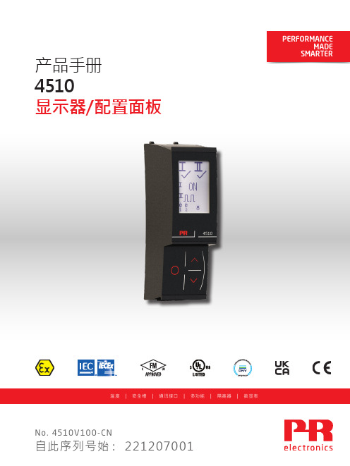
产品手册4510显示器/配置面板温度 | 安全栅 | 通讯接口 | 多功能 | 隔离器 | 数显表No. 4510V100-CN自此序列号始: 2212070016 大特色产品 满足您的一切需求采用创新型专利技术,信号调节更加简单智能。
产品组合由六大类别组成,具备多种模拟量和数字量模块,涵盖上千种工业自动化应用。
所有产品均符合甚至超越行业的最高标准。
这可确保产品即便在最恶劣的环境条件下仍能可靠运行。
5 年产品保修期,让您使用更安心。
单品出色,组合无敌温度变送器和温度传感器系列产品,提供从温度测量点到系统控制一站式信号解决方案,从而在最大程度上保证信号的完整性。
仅需一套点对点解决方案,您就可以在任何环境中将工业过程中的温度信号转换为模拟量信号、总线信号或数字通讯信号。
该方案具备响应时间短,自动校准,传感器故障检测,低漂移和卓越 EMC 性能等诸多优点。
单品为多功能系列产品,可兼容大量现场应用,可轻而易举按照您的现场标准进行配置。
此种单品可适应多种应用方式,既能节省安装和培训时间,又能大大简化库存备件管理。
该设备经过精心打造,其长期信号精度高、功耗低、抗电噪声优异、易于编程。
我们提供经济实惠、使用方便、面向未来的通讯接口,以便您能够访问所安装的 PR 产品。
所有接口均可拆卸,并带有屏幕和按钮,可以显示过程值/诊断值和对参数进行配置。
产品特定功能包括通过 Modbus 和蓝牙进行通讯,以及使用我们的 PR 过程主管 (PPS) 应用进行远程访问,可用于 iOS 和 Android 等终端。
数显表系列以其灵活性和稳定性著称。
该设备系列几乎满足过程信号读数显示的所有需求并具备通用型输入和供电能力。
无论哪种行业,无论环境条件何其苛刻,该设备均能实时测量过程值并提供用户友好型界面和值得信赖的继电器信号。
我们采用最严格的安全标准来检验产品,以期提供最安全的信号。
秉承创新精神,我们已经在 SIL 2 全面评估本质安全型接口方面取得了开创性成就,其既高效又经济,效果卓著,成效斐然。
NE5210中文手册

NE5210(280MHz)一、PIN配置二、描述NE5210是7 kΩ互阻抗宽频带,微分输出的低噪声放大器。
特别适合信号恢复光纤接收器。
一部分是适合很多其他射频程序作为一个通用获得块。
三、特性•低噪声:3.5 pa / /赫兹•单5 v电源•大带宽:280 mhz•微分输出•输入/输出阻抗低•高电源抑制比•高过载阈值电流•宽动态范围•7 kw微分互阻四、应用•光纤接收器,模拟计算机和数字计算机两种•电流电压转换器•宽带增益块•医学和科学仪器•传感器放大器•单端微分转换•低噪声射频放大器•射频信号处理五、应用信息0 到 +70 C六、绝对最大额定参数1、最大耗散是由操作环境温度和热阻决定的:qJA = 125°C / W。
2、建议使用一个上拉电阻VCC PIN二极管七、推荐的操作条件八、直流电特性最小和最大限制适用于工作温度范围在VCC = 5 v,除非另有说明。
典型的1.测试条件:输出静电压变化小于100 mv 3 mA负载电流。
R/V VCC=50.5V R/T TA=TA MAX-TA MIN %/ C f=10MHz, TA=25 C 测试电路2 pA/HzTA=25 C 测试电路2 f=100MHz f=200MHz f=300MHz f=100MHz f=200MHz f=300MHz(VCC1=VCC2) 直流测试,VCC=0.1V ,等效交流测试电路3直流测试,VCC=0.1V ,等效交流测试电路4直流测试,VCC=0.1V ,等效交流测试电路5九、交流电特性(连续的)1.寄生电容相当于约0.2 pf2.PSRR是依赖于输出引用和电路板布局在更高的频率。
最佳性能在VCC线使用射频滤波器3.保证了线性和过载测试。
4.tR上升时间定义为20 - 80%。
它保证了3 db带宽测试。
十、测试电路:测试电路2:测试电路3(连续的):测试电路4(连续的):测试电路5(连续的):测试电路6(连续的):测试电路7:十一、典型的差分输出电压和输入电流十二、NE5210测试条件:步骤1:RT在 60 A 测量RT = (VO1 – VO2)/(+60 A – (–60A))VO1在t IIN = +60A测量VO2在t IIN = –60A测量步骤2:线性度= 1 – ABS((VOA – VOB) / (VO3 – VO4))VO3 在 IIN = +120A测量VO4在 IIN = –120A测量VOA _ RT _ (_ 120_A) _ VOBVOB _ RT _ (_ 120_A) _ VOB步骤3:VOMAX = VO7 – VO8VO7 在 IIN = +260A测量VO8 在 IIN = –260A测量步骤4:IIN 测试条件VO7 – VO5 > 20mV and V06 – VO5 > 20mVVO5 在 IIN = +160A测量VO6 在 IIN = –160A测量VO7在 IIN = +260A测量VO8 在 IIN = –260A测量十三、典型的性能特性NE5210电源电流和温度的关系如图:NE5210输出偏置电压和温度的关系如图:输出电压与输入电流的关系如图:NE5210输入偏置电压与温度的关系如图:NE5210输出偏置电压与温度的关系如图:微分输出电压和输入电流的关系如图:NE5210输出偏置电压与温度的关系如图:NE5210微分输出摆动与温度的关系如图:微分输出电压与输入电流的关系如图:增益与频率:NE5210微分互阻与温度:NE5210带宽与温度:增益和相位偏移与频率的关系:NE5210典型的带宽分布:NE5210输出电阻与温度:输出电阻与频率的关系如图:NE5210电源供应拒绝比例与温度的关系:群延时:输出阶跃响应:十四、工作原理阻抗放大器被广泛用作前置放大器光纤接收器。
tmc2210中文规格书

tmc2210中文规格书TMC2210中文规格书一、产品介绍TMC2210是一款先进的步进电机驱动器,具有高性能和高精度的特点。
该驱动器采用了最新的技术,为用户提供了更好的驱动体验。
TMC2210适用于各种领域,如工业自动化、机器人、3D打印等。
二、主要特点1. 高精度:TMC2210采用了先进的运动控制算法,能够实现高精度的步进电机驱动,确保运动的平稳和准确性。
2. 低噪音:该驱动器通过改进的电流控制和电机驱动技术,降低了噪音水平,提供了更加安静的工作环境。
3. 高效能:TMC2210的电源效率非常高,能够最大程度地利用电能,减少能源浪费。
4. 多种保护功能:该驱动器具有过流保护、过温保护、欠压保护等多种保护功能,可以有效保护电机和驱动器的安全运行。
5. 简化设计:TMC2210的设计紧凑,可以方便地集成到各种设备中,简化了系统的设计和安装。
三、技术参数1. 电源电压范围:5V-28V2. 驱动电流:最大2.5A3. 步进角度:1.8°4. 步进分辨率:最大256微步5. 控制接口:SPI、UART6. 工作温度范围:-40°C至+85°C7. 封装形式:QFN48四、应用领域TMC2210广泛应用于各种领域,包括:1. 工业自动化:TMC2210可以用于控制各种工业设备,如数控机床、印刷机、包装机等。
2. 机器人:该驱动器可以用于机器人的关节控制,提供高精度和高效能的驱动能力。
3. 3D打印:TMC2210可以用于3D打印机的各个轴的驱动,实现高精度和高速度的打印。
五、总结TMC2210是一款高性能的步进电机驱动器,具有高精度、低噪音和高效能的特点。
该驱动器适用于工业自动化、机器人和3D打印等领域。
它的多种保护功能和简化设计使其成为用户的首选。
希望通过本规格书的介绍,能够使用户更好地了解TMC2210的特点和应用。
NUP4202W1T2G中文资料

NUP4202W1Low Capacitance SC−88Diode−TVS Array for High Speed Data Lines ProtectionThe NUP4202W1 transient voltage suppressor is designed to protect high speed data lines from ESD, EFT, and lightning.Features:•Low Capacitance (3 pF Maximum Between I/O Lines)•ESD Rating of Class 3B (Exceeding 8 kV) per Human Body model and Class C (Exceeding 400 V) per Machine Model •Protection for the Following IEC Standards:IEC 61000−4−2 (ESD) 15 kV (air) 8 kV (contact)IEC 61000−4−4 (EFT) 40 A (5/50 ns)IEC 61000−4−5 (Lightning) 23 A (8/20 m s)•UL Flammability Rating of 94 V−0•This is a Pb−Free DeviceTypical Applications:•High Speed Communication Line Protection •USB 1.1 and 2.0 Power and Data Line Protection •Digital Video Interface (DVI) and HDMI •Monitors and Flat Panel Displays •MP3MAXIMUM RATINGS (T J = 25°C unless otherwise noted)RatingSymbol Value Unit Peak Power Dissipation8 x 20 m S @ T A = 25°C (Note 1)P pk 500W Operating Junction Temperature Range T J −40 to +125°C Storage Temperature Range T stg −55 to +150°C Lead Solder Temperature −Maximum (10 Seconds)TL 260°C Human Body Model (HBM)Machine Model (MM)IEC 61000−4−2 Air (ESD)IEC 61000−4−2 Contact (ESD)ESD160004002000020000VStresses exceeding Maximum Ratings may damage the device. Maximum Ratings are stress ratings only. Functional operation above the Recommended Operating Conditions is not implied. Extended exposure to stresses above the Recommended Operating Conditions may affect device reliability.1.Nonrepetitive current pulse per Figure 1 (Pin 5 to Pin 2)Device PackageShippingORDERING INFORMATIONNUP4202W1T2GSC−88(Pb−Free)3000/Tape & Reel †For information on tape and reel specifications,including part orientation and tape sizes, please refer to our Tape and Reel Packaging Specification Brochure, BRD8011/D.ELECTRICAL CHARACTERISTICS (T J =25°C unless otherwise specified)ParameterSymbol ConditionsMinTypMax Unit Reverse Working Voltage V RWM (Note 2)5.0V Breakdown Voltage V BR I T = 1 mA, (Note 3) 6.0V Reverse Leakage Current I R V RWM = 5 V 5.0m A Clamping Voltage V C I PP = 5 A (Note 4)8.512.5V Clamping VoltageV C I PP = 8 A (Note 4)8.920V Maximum Peak Pulse Current IPP 8x20 m s Waveform28A Junction Capacitance C J V R = 0 V, f = 1 MHz between I/O Pins and GND 3.0 5.0pF Junction CapacitanceC JV R = 0 V, f = 1 MHz between I/O Pins1.5 3.0pFS devices are normally selected according to the working peak reverse voltage (V RWM ), which should be equal or greater than the DC or continuous peak operating voltage level.3.V BRis measured at pulse test current I T .4.Nonrepetitive current pulse per Figure 1 (Pin 5 to Pin 2)TYPICAL PERFORMANCE CURVES(T J = 25°C unless otherwise noted)Figure 1. Pulse Derating Curve1009080706050403020100T A , AMBIENT TEMPERATURE (°C)Figure 2. 8 × 20 m s Pulse Waveform1009080706050403020100t, TIME (m s)% O F P E A K P U L S E C U R R E N TFigure 3. Junction Capacitance vs Reverse Voltage5.02.50.0V BR , REVERSE VOLTAGE (V)J U N C T I O N C A P A C I T A N C E (p F )P E A K P O W E R D I S S I P A T I O N (%)4.52.04.01.53.51.03.00.5Figure 4. Clamping Voltage vs. Peak Pulse Current(8 x 20 m s Waveform)20100010PEAK PULSE CURRENT (A)C L A M P I N G V O L T A G E (V )20304050188166144122APPLICATIONS INFORMATIONThe new NUP4202W1 is a low capacitance TVS diode array designed to protect sensitive electronics such as communications systems, computers, and computer peripherals against damage due to ESD events or transient overvoltage conditions. Because of its low capacitance, it can be used in high speed I/O data lines. The integrated design of the NUP4202W1 offers surge rated, low capacitance steering diodes and a TVS diode integrated in a single package (SC−88). If a transient condition occurs, the steering diodes will drive the transient to the positive rail of the power supply or to ground. The TVS device protects the power line against overvoltage conditions to avoid damage to the power supply and any downstream components.NUP4202W1 Configuration OptionsThe NUP4202W1 is able to protect up to four data lines against transient overvoltage conditions by driving them to a fixed reference point for clamping purposes. The steering diodes will be forward biased whenever the voltage on the protected line exceeds the reference voltage (Vf or Vcc+Vf).The diodes will force the transient current to bypass the sensitive circuit.Data lines are connected at pins 1, 3, 4 and 6. The negative reference is connected at pin 2. This pin must be connected directly to ground by using a ground plane to minimize the PCB’s ground inductance. It is very important to reduce the PCB trace lengths as much as possible to minimize parasitic inductances.Option 1Protection of four data lines and the power supply using Vcc as reference.I/O 1I/O 2I/O 3I/O 4For this configuration, connect pin 5 directly to the positive supply rail (Vcc), the data lines are referenced to the supply voltage. The internal TVS diode prevents overvoltage on the supply rail. Biasing of the steering diodes reduces their capacitance.Option 2Protection of four data lines with bias and power supply isolation resistor.The NUP4202W1 can be isolated from the power supply by connecting a series resistor between pin 5 and Vcc. A10 k W resistor is recommended for this application. This will maintain a bias on the internal TVS and steering diodes,reducing their capacitance.Option 3Protection of four data lines using the internal TVS diode as reference.In applications lacking a positive supply reference or those cases in which a fully isolated power supply is required, the internal TVS can be used as the reference. For these applications, pin 5 is not connected. In this configuration, the steering diodes will conduct whenever the voltage on the protected line exceeds the working voltage of the TVS plus one diode drop (Vc=Vf + V TVS ).ESD Protection of Power Supply LinesWhen using diodes for data line protection, referencing to a supply rail provides advantages. Biasing the diodes reduces their capacitance and minimizes signal distortion.Implementing this topology with discrete devices does have disadvantages. This configuration is shown below:Looking at the figure above, it can be seen that when a positive ESD condition occurs, diode D1 will be forward biased while diode D2 will be forward biased when a negative ESD condition occurs. For slower transient conditions, this system may be approximated as follows: For positive pulse conditions:Vc = Vcc + Vf D1For negative pulse conditions:Vc = −Vf D2ESD events can have rise times on the order of some number of nanoseconds. Under these conditions, the effect of parasitic inductance must be considered. A pictorial representation of this is shown below.An approximation of the clamping voltage for these fast transients would be:For positive pulse conditions:Vc = Vcc + Vf + (L di ESD/dt)For negative pulse conditions:Vc = −Vf – (L di ESD/dt)As shown in the formulas, the clamping voltage (Vc) not only depends on the Vf of the steering diodes but also on the L di ESD/dt factor. A relatively small trace inductance can result in hundreds of volts appearing on the supply rail. This endangers both the power supply and anything attached to that rail. This highlights the importance of good board layout. Taking care to minimize the effects of parasitic inductance will provide significant benefits in transient immunity.Even with good board layout, some disadvantages are still present when discrete diodes are used to suppress ESD events across datalines and the supply rail. Discrete diodes with good transient power capability will have larger die and therefore higher capacitance. This capacitance becomes problematic as transmission frequencies increase. Reducing capacitance generally requires reducing die size. These small die will have higher forward voltage characteristics at typical ESD transient current levels. This voltage combined with the smaller die can result in device failure.The ON Semiconductor NUP4202W1 was developed to overcome the disadvantages encountered when using discrete diodes for ESD protection. This device integrates aTVS diode within a network of steering diodes.NUP4202W1 Equivalent CircuitDuring an ESD condition, the ESD current will be drivento ground through the TVS diode as shown below.ESDposThe resulting clamping voltage on the protected IC will be:Vc = V F + V TVS.The clamping voltage of the TVS diode is provided in Figure 4 and depends on the magnitude of the ESD current. The steering diodes are fast switching devices with unique forward voltage and low capacitance characteristics.TYPICAL APPLICATIONSUPSTREAM USB PORTDOWNSTREAM USB PORTDOWNSTREAM USB PORTESD Protection for USB PortProtection for Ethernet 10/100 (Differential mode)RJ45TI/E1 Interface ProtectionPACKAGE DIMENSIONSNOTES:1.DIMENSIONING AND TOLERANCING PER ANSI Y14.5M, 1982.2.CONTROLLING DIMENSION: INCH.3.419B−01 OBSOLETE, NEW STANDARD 419B−02.SC−88/SC70−6/SOT−363CASE 419B−02ISSUE VDIM MIN NOM MAX MILLIMETERS A 0.800.95 1.10A10.000.050.10A3b 0.100.210.30C 0.100.140.25D 1.80 2.00 2.200.0310.0370.0430.0000.0020.0040.0040.0080.0120.0040.0050.0100.0700.0780.086MINNOM MAX INCHES0.20 REF 0.008 REF H EE 1.15 1.25 1.35e 0.65 BSC L 0.100.200.302.00 2.10 2.200.0450.0490.0530.026 BSC0.0040.0080.0120.0780.0820.086*For additional information on our Pb−Free strategy and solderingdetails, please download the ON Semiconductor Soldering and Mounting Techniques Reference Manual, SOLDERRM/D.SOLDERING FOOTPRINT*ON Semiconductor and are registered trademarks of Semiconductor Components Industries, LLC (SCILLC). SCILLC reserves the right to make changes without further notice to any products herein. SCILLC makes no warranty, representation or guarantee regarding the suitability of its products for any particular purpose, nor does SCILLC assume any liability arising out of the application or use of any product or circuit, and specifically disclaims any and all liability, including without limitation special, consequential or incidental damages.“Typical” parameters which may be provided in SCILLC data sheets and/or specifications can and do vary in different applications and actual performance may vary over time. All operating parameters, including “Typicals” must be validated for each customer application by customer’s technical experts. SCILLC does not convey any license under its patent rights nor the rights of others. SCILLC products are not designed, intended, or authorized for use as components in systems intended for surgical implant into the body, or other applications intended to support or sustain life, or for any other application in which the failure of the SCILLC product could create a situation where personal injury or death may occur. Should Buyer purchase or use SCILLC products for any such unintended or unauthorized application, Buyer shall indemnify and hold SCILLC and its officers, employees, subsidiaries, affiliates, and distributors harmless against all claims, costs, damages, and expenses, and reasonable attorney fees arising out of, directly or indirectly, any claim of personal injury or death associated with such unintended or unauthorized use, even if such claim alleges that SCILLC was negligent regarding the design or manufacture of the part. SCILLC is an Equal Opportunity/Affirmative Action Employer. This literature is subject to all applicable copyright laws and is not for resale in any manner.PUBLICATION ORDERING INFORMATION。
- 1、下载文档前请自行甄别文档内容的完整性,平台不提供额外的编辑、内容补充、找答案等附加服务。
- 2、"仅部分预览"的文档,不可在线预览部分如存在完整性等问题,可反馈申请退款(可完整预览的文档不适用该条件!)。
- 3、如文档侵犯您的权益,请联系客服反馈,我们会尽快为您处理(人工客服工作时间:9:00-18:30)。
RECEIVERNR4210 Series
InAlAs APD RECEIVER WITH INTERNAL PRE-AMPLIFIER FOR 10 Gb/s APPLICATIONS
Document No. PL10637EJ01V0DS (1st edition) Date Published September 2006 NS CP(K)
DESCRIPTION The NR4210 Series products consist of InAIAs-APD (avalanche photo diode) ROSAs (Receiver Optical Sub-Assembly) with internal pre-amplifiers designed for 10 Gb/s long-reach optical transceivers such as the XENPAK/X2/XFP. These modules are ideal as receivers for IEEE 10G BASE and SONET OC-192 systems.
FEATURES • XMD-MSA compliant ROSA • 10 Gb/s high sensitivity InAlAs-APD • +3.3 V SiGe transimpedance pre-amplifier • Minimum receiver sensitivity Pr = −28 dBm
• Operating case temperature TC = −5 to +85°C
• Transimpedance Zt = 2 000 Ω (Single-ended)
• Cut-off frequency fc = 8 GHz • With flexible printed circuit
2006
元器件交易网www.cecb2b.comNR4210 SeriesPACKAGE DIMENSIONS (UNIT: mm)
4.64±0.05φ7.0±0.1φ
11.51+0.1 –0.1516.5±0.3
5.5±0.02φ
OPTICALREFERENCEPLANE
2.4±0.1
6.6±0.1
(2.51)
OFF-SET(0.2)
BOTTOM VIEWNR4210TF
4.7±0.1φ5.6 MAX.φ16.2
5.83.013.2
2.0
5.65–0.796–0.350.27NCGNDDATA NDATA PGNDVCC
Vapd
Rth
Preliminary Data Sheet PL10637EJ01V0DS 2
元器件交易网www.cecb2b.comNR4210 Series5.0±0.1φ
8.7+0.1 –0.1514.0±0.35.5±0.02φ
5.83.013.2
2.0
5.65–0.796–0.350.27NCGNDDATA NDATA PGNDVCC
OPTICALREFERENCEPLANE
5.6 MAX.φ1.3
OFF-SET(0.2)
BOTTOM VIEWNR4210TG
4.053.5±0.022.92±0.01φ
1.350.55±0.03
5.15±0.
0
5
16.2Vapd
Rth
φ
Preliminary Data Sheet PL10637EJ01V0DS 3
元器件交易网www.cecb2b.comNR4210 Series5.0±0.1φ7.512.7±0.35.5±0.02φ
5.83.017.2
2.0
5.65–0.796–0.350.27NCGNDDATA NDATA PGNDVCC
OPTICALREFERENCEPLANE
5.6 MAX.φ
OFF-SET(0.2)
BOTTOM VIEW
NR4210TK
4.053.8±0.020.55±0.03
5.15±0.
0
5
20.2Vapd
Rth
2.99±0.01φφ
Preliminary Data Sheet PL10637EJ01V0DS 4
元器件交易网www.cecb2b.comNR4210 Series
5.83.017.2
2.0
5.65–0.796–0.350.27NCGNDDATA NDATA PGNDVCC
BOTTOM VIEW
NR4210TL20.2Vapd
Rth
5.0±0.1φ8.7+0.1 –0.1514.0±0.35.5±0.02φ
OPTICALREFERENCEPLANE
5.6 MAX.φ1.3
OFF-SET(0.2)
4.05
3.5±0.022.92±0.01φ
1.350.55±0.03
5.15±0.
0
5
φ
Preliminary Data Sheet PL10637EJ01V0DS 5
元器件交易网www.cecb2b.comNR4210 Series5.0±0.1φ
7.512.7±0.35.5±0.02φ
5.83.013.2
2.0
5.65–0.796–0.350.27NCGNDDATA NDATA PGNDVCC
OPTICALREFERENCEPLANE
5.6 MAX.φ
OFF-SET(0.2)
BOTTOM VIEWNR4210TP
4.053.8±0.022.99±0.01φ0.
5
5±0.035.15±0.
0
5
16.2Vapd
Rth
φ
Preliminary Data Sheet PL10637EJ01V0DS 6
元器件交易网www.cecb2b.com