LM5105
骨科疾病编码
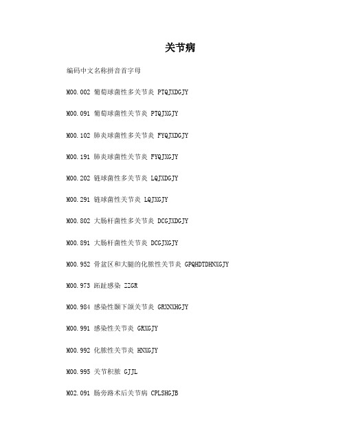
关节病编码中文名称拼音首字母M00.002 葡萄球菌性多关节炎 PTQJXDGJYM00.091 葡萄球菌性关节炎 PTQJXGJYM00.102 肺炎球菌性多关节炎 FYQJXDGJYM00.191 肺炎球菌性关节炎 FYQJXGJYM00.202 链球菌性多关节炎 LQJXDGJYM00.291 链球菌性关节炎 LQJXGJYM00.802 大肠杆菌性多关节炎 DCGJXDGJYM00.891 大肠杆菌性关节炎 DCGJXGJYM00.952 骨盆区和大腿的化脓性关节炎 GPQHDTDHNXGJY M00.973 跖趾感染 ZZGRM00.984 感染性颞下颌关节炎 GRXNXHGJYM00.991 感染性关节炎 GRXGJYM00.992 化脓性关节炎 HNXGJYM00.995 关节积脓 GJJLM02.091 肠旁路术后关节病 CPLSHGJBM02.191 痢疾后关节病 LJHGJBM02.291 血清性关节炎 XQXGJYM02.301 莱特尔(尿道炎-结膜炎-关节炎)综合征 LTENDYJMYGJYZHZM02.891 其他反应性关节病 QTFYXGJBM02.901 反应性关节病在其他方面未特指 FYXGJBM05.001 类风湿性关节炎合并脾大和白细胞减少[费尔蒂综合征] LFSXGJYHBPDHBXBJSFED M05.101+ 类风湿疾病肺改变 LFSJBFGBM05.102+ 类风湿性肺泡炎 LFSXFPYM05.103+ 类风湿性弥漫性肺间质纤维化 LFSXMMXFJZXWHM05.104+ 类风湿性纤维化肺泡炎M05.105+ 类风湿尘肺[卡普兰综合征] LFSCFKPLZHZM05.106+ 类风湿性肺病 LFSXFBM05.201 类风湿性脉管炎 LFSXMGYM05.301 累及内脏的类风湿性关节炎 LJNZDLFSXGJYM05.302 累及全身的类风湿性关节炎 LJQSDLFSXGJYM05.303+ 类风湿性关节炎性心肌病 LFSXGJYXXJB M05.304+ 类风湿性多神经病 LFSXDSJB M05.305+ 类风湿性心肌病 LFSXXJBM05.306+ 类风湿性关节炎伴心包炎 LFSXGJYBXBYM05.307+ 类风湿性心肌炎 LFSXXJYM05.308+ 类风湿性心脏病 LFSXXZBM05.309+ 类风湿性关节炎伴心炎 LFSXGJYBXYM05.951 血清反应阳性的类风湿性关节炎在其他方面未特指 XQFYYXDLFSXGJYM06.001 血清反应阴性的类风湿性关节炎 XQFYYXDLFSXGJYM06.191 成年型斯蒂尔病或综合征[成人型类风湿性关节炎] CNXSDEBHZHZCRXLFSXGJM06.291 类风湿性粘液囊炎 LFSXNYNYM06.391 类风湿性结节 LFSXJJM06.401 炎性多关节病 YXDGJBM06.881 其他特指的类风湿性关节炎 QTTZDLFSXGJYM06.981 类风湿性颞下颌关节炎 LFSXNXHGJYM06.991 类风湿性关节炎在其他方面未特指 LFSXGJYM08.001 幼年型全身性类风湿性关节炎[变应性亚败血症] YNXQSXLFSXGJYBYXYBXZ M08.101 幼年型关节强硬性脊椎炎 YNXGJQYXJZYM08.202 幼年型全身性关节炎[斯蒂尔氏病] YNXQSXGJYSDESBM08.203 幼年型关节炎伴全身性发病 YNXGJYBQSXFBM08.291 斯蒂尔病 SDEBM08.301 儿童类风湿病,多关节型 ETLFSBDGJXM08.302 幼年型多关节炎(血清反应阴性) YNXDGJYXQFYYX M08.393 慢性幼年型关节炎 MXYNXGJYM08.491 少关节性幼年型关节炎 SGJXYNXGJYM08.891 其他幼年型关节炎 QTYNXGJYM08.991 幼年型关节炎在其他方面未特指 YNXGJYM10.091 痛风石 TFS M10.092 痛风性关节炎 TFXGJYM10.093 痛风性滑囊炎 TFXHNYM10.094+ 心痛风石 XTFS M10.095 特发性痛风 TFXTFM10.096 痛风性粘液囊炎 TFXNYNYM10.097 原发性痛风 YFXTFM10.191 铅性痛风 QXTFM10.291 药物性痛风 YWXTFM10.391 痛风性肾病 TFXSBM10.392 痛风性肾结石 TFXSJSM10.495 其他继发性痛风 QTJFXTFM10.991 痛风在其他方面未特指 TFM10.992 痛风结节 TFJJ M10.993+ 耳痛风石 ETFSM11.095 羟磷灰石沉着病 QLHSCZBM11.195 家族性软骨钙沉着 JZXRGGCZM11.291 软骨钙沉着在其他方面未特指 RGGCZM11.885 其他特指的晶体性关节病QTTZDJTXGJBM11.995 晶体性关节病在其他方面未特指JTXGJBM12.095 雅库氏综合征[慢性风湿病后关节病] YKSZHZMXFSBHGJB M12.191 大骨节病[卡斯钦-贝克病] DGJBKSQBKBM12.291 绒毛结节状滑膜炎(色素沉着的) RMJJZHMYSSCZDM12.395 复发性风湿病FFXFSBM12.495 间歇性关节积液(水) JXXGJJYSM12.585 创伤性颞下颌关节炎(病) CSXNXHGJYBM12.595 创伤性关节炎(病) CSXGJYBM12.891 短暂性关节炎DZXGJYM13.051 多关节炎在其他方面未特指DGJYM13.155 髋关节炎KGJYM13.195 单关节炎 NEC DGJYM13.805 幼年型多关节炎YNXDGJYM13.885 颞下颌关节炎NXHGJYM13.891 变应性关节炎BYXGJYM13.895 更年期关节炎GNQGJYM13.896 退变性关节炎TBXGJYM13.991 关节炎(病) 在其他方面未特指 GJYBM15.005 原发性全身性(骨)关节病YFXQSXGGJBM15.195 赫伯登结节(伴关节病) HBDJJBGJBM15.295 沙尔结节(伴关节病) SEJJBGJBM15.305 继发性多发性关节病JFXDFXGJBM15.306 创伤后多关节病CSHDGJBM15.495 侵蚀性(骨)关节病QSXGGJBM15.805 海加思结节HJSJJM15.806 其他多关节病QTDGJBM15.905 慢性多发性对称性骨关节病MXDFXDCXGGJBM15.906 全身性骨关节病(炎)黄子孙在其他方面未特指QSXGGJBYHZS M16.055 原发性双侧髋关节病YFXSCKGJBM16.155 原发性单侧髋关节病YFXDCKGJBM16.255 发育异常引起的双侧髋关节病FYYCYQDSCKGJBM16.355 发育异常性单侧髋关节病FYYCXDCKGJBM16.455 创伤后双侧髋关节病CSHSCKGJBM16.555 创伤后单侧髋关节病CSHDCKGJBM16.655 继发性双侧髋关节病JFXSCKGJBM16.755 继发性单侧髋关节病JFXDCKGJBM16.951 髋关节病在其他方面未特指KGJBM17.065 原发性双侧膝关节病YFXSCXGJBM17.165 原发性单侧膝关节病YFXDCXGJBM17.265 创伤后双侧膝关节病CSHSCXGJBM17.365 创伤后单侧膝关节病CSHDCXGJBM17.465 其他继发性双侧膝关节病QTJFXSCXGJBM17.565 继发性单侧膝关节病JFXDCXGJBM17.961 膝关节病在其他方面未特指XGJBM18.045 双侧第一腕掌关节的原发性关节病SCDYWZGJDYFXGJBM18.145 单侧第一腕掌关节的原发性关节病DCDYWZGJDYFXGJBM18.245 双侧第一腕掌关节的创伤后关节病SCDYWZGJDCSHGJBM18.345 单侧第一腕掌关节的创伤后关节病DCDYWZGJDCSHGJBM18.445 双侧第一腕掌关节的继发性关节病SCDYWZGJDJFXGJBM18.545 单侧第一腕掌关节的继发性关节病DCDYWZGJDJFXGJBM18.945 第一腕掌关节的关节病在其他方面未特指DYWZGJDGJBM19.095 原发性关节病在其他方面未特指YFXGJBM19.195 创伤后关节病在其他方面未特指CSHGJBM19.295 继发性关节病在其他方面未特指JFXGJBM19.821 肘骨关节病ZGGJBM19.841 指骨关节病ZGGJBM19.895 其他特指关节病QTTZGJBM19.935 双侧腕骨性关节炎(病) SCWGXGJYBM19.955 双侧髋关节骨性关节炎(病) SCKGJGXGJYB M19.965 老年性膝关节炎(病) LNXXGJYBM19.966 双侧膝骨性关节炎(病) SCXGXGJYBM19.975 双侧踝关节骨性关节炎(病) SCHGJGXGJYB M19.991 骨关节病GGJB M19.995 肥大性关节炎[骨关节炎] FDXGJYGGJYM19.996 局限性关节病JXXGJBM19.997 骨性(病)关节炎GXBGJYM20.041 后天性槌状指HTXCZZM20.042 后天性指畸形HTXZJXM20.045 后天性小指屈曲畸形HTXXZQQJXM20.046 后天性手畸形HTXSJXM20.047 后天性指挛缩畸形HTXZLSJXM20.171 拇囊炎(足) MNYZM20.172 后天性拇外翻HTXMWFM20.275 僵拇(足) JMZM20.371 后天性拇(足)内翻HTXMZNFM20.375 拇(足)内翻MZNFM20.376 拇(足)变形(后天性) MZBXHTXM20.475 其他后天性锤状趾QTHTXCZZM20.571 足仰趾畸形ZYZJXM20.671 后天性趾畸形在其他方面未特指HTXZJX M21.021 后天性肘外翻HTXZWFM21.061 后天性膝外翻HTXXWFM21.071 后天性马蹄外翻足HTXMTWFZM21.072 后天性足外翻HTXZWFM21.121 后天性肘内翻HTXZNFM21.151 后天性髋内翻HTXKNFM21.161 后天性膝内翻HTXXNFM21.171 后天性足内翻HTXZNFM21.225 后天性肘关节屈曲畸形HTXZGJQQJXM21.261 后天性膝关节屈曲畸形HTXXGJQQJXM21.335 后天性腕下垂HTXWXCM21.371 后天性足下垂HTXZXCM21.471 扁平足[平足](后天性) BPZPZHTXM21.545 手爪形SZXM21.571 后天性高弓足HTXGGZM21.575 后天性足畸形HTXZJXM21.576 仰趾弓形足(爪形趾) YZGXZZXZM21.671 足后天畸形ZHTJXM21.785 后天性四肢长度不等HTXSZCDBDM21.815 后天性翼状肩胛骨HTXYZJJGM21.851 后天性股骨畸形HTXGGJXM21.935 后天性腕关节畸形HTXWGJJXM21.951 后天性髋关节畸形HTXKGJJXM21.981 后天性下肢畸形HTXXZJXM21.995 后天性关节畸形HTXGJJXM22.065 习惯性复发性髌骨脱位XGXFFXBGTW M22.165 复发性髌骨不全脱位FFXBGBQTWM22.205 髌股疾患BGJHM22.365 髌骨其他紊乱BGQTWLM22.461 髌骨软骨软化BGRGRHM22.865 髌骨其他疾患BGQTJHM22.965 髌骨疾患在其他方面未特指BGJH M23.061 膝外侧半月板囊肿XWCBYBNZM23.091 膝半月板囊肿XBYBNZM23.095 膝关节囊肿XGJNZM23.191 先天性盘状半月板XTXPZBYBM23.231 陈旧性膝内侧半月板损伤CJXXNCBYBSSM23.235 陈旧性半月板内侧桶柄样撕裂CJXBYBNCTBYSL M23.261 陈旧性膝外侧半月板损伤CJXXWCBYBSSM23.291 陈旧性半月板损伤CJXBYBSSM23.295 陈旧性膝关节韧带损伤CJXXGJRDSSM23.315 内侧半月板前角紊乱NCBYBQJWLM23.325 内侧半月板后角紊乱NCBYBHJWLM23.335 内侧半月板紊乱NCBYBWLM23.365 陈旧性外侧半月板紊乱CJXWCBYBWLM23.395 膝关节变性XGJBXM23.396 病理性关节脱位BLXGJTWM23.491 膝关节游离体XGJYLTM23.595 膝慢性不稳定性疾患XMXBWDXJHM23.695 膝韧带其他自然破裂XRDQTZRPLM23.895 膝韧带松弛XRDSCM23.896 半月板钙化BYBGHM23.897 弹响膝DXXM23.995 半月板疾患在其他方面未特指 BYBJH M23.996 膝内部紊乱在其他方面未特指 XNBWL M24.091 关节内游离体GJNYLTM24.195 其他关节软骨疾患QTGJRGJHM24.281 项韧带肥厚XRDFHM24.291 黄韧带肥厚HRDFHM24.292 韧带钙化RDGHM24.295 韧带囊肿RDNZM24.296 韧带松弛RDSCM24.351 髋关节病理性脱位KGJBLXTWM24.361 膝关节病理性脱位XGJBLXTWM24.391 关节病理性脱位GJBLXTWM24.392 关节自发性脱位GJZFXTWM24.465 膝韧带囊肿XRDNZM24.491 关节习惯性脱位GJXGXTWM24.535 腕关节屈曲挛缩WGJQQLSM24.551 髋关节屈曲挛缩(后天性) KGJQQLSHTX M24.565 膝反屈XFQM24.591 关节挛缩GJLSM24.595 关节弯曲GJWQM24.621 肘关节强硬ZGJQYM24.645 指间关节强直ZJGJQZM24.651 髋关节强硬KGJQYM24.661 膝关节强硬XGJQYM24.671 踝关节强硬HGJQYM24.685 颞颌关节强硬NHGJQYM24.691 关节强硬GJQYM24.755 髋臼前突KJQTM24.811 陈旧性肩关节脱位CJXJGJTWM24.855 髋关节紊乱KGJWLM24.856 应激性髋YJXKM24.861 陈旧性髌骨脱位CJXBGTWM24.885 腰椎关节紊乱YZGJWLM24.891 关节粘连GJNLM24.995 关节紊乱在其他方面未特指GJWLM25.091 关节积血GJJXM25.195 关节瘘GJLM25.295 关节松弛GJSCM25.395 关节其他不稳定性疾患GJQTBWDXJHM25.491 关节积液GJJYM25.505 多关节痛DGJTM25.506 痛痛病(骨和关节的及四肢痛疼) TTBGHGJDJSZTT M25.511 肩关节痛JGJTM25.551 髋关节痛KGJTM25.561 膝关节痛XGJTM25.591 关节痛GJTM25.661 膝关节僵硬XGJJYM25.681 肢体僵硬ZTJYM25.691 关节僵硬GJJYM25.795 骨赘GZM25.891 关节肿胀GJZZM25.892 关节周围骨化GJZWGHM25.895 其他特指关节疾患难QTTZGJJHNM25.991 关节病GJBM25.992 关节肿物GJZW骨病和软骨病编码中文名称拼音首字母M80.095 绝经后骨质疏松伴病理性骨折JJHGZSSBBLXGZM80.195 卵巢切除术后骨质疏松伴病理性骨折LCQCSHGZSSBBLXGZM80.295 废用性骨质疏松伴病理性骨折FYXGZSSBBLXGZM80.395 手术后吸收障碍性骨质疏松伴病理性骨折SSHXSZAXGZSSBBLXGZ M80.495 药物性骨质疏松伴病理性骨折YWXGZSSBBLXGZM80.595 特发性骨质疏松伴病理性骨折TFXGZSSBBLXGZM80.895 其他骨质疏松伴病理性骨折QTGZSSBBLXGZM80.995 骨质疏松伴病理性骨折在其他方面未特指GZSSBBLXGZM81.095 绝经后骨质疏松JJHGZSSM81.195 卵巢切除术后骨质疏松LCQCSHGZSSM81.295 废用性骨质疏松FYXGZSSM81.395 手术后吸收障碍性骨质疏松SSHXSZAXGZSS M81.495 药物诱发性骨质疏松YWYFXGZSSM81.595 特发性骨质疏松TFXGZSSM81.695 局限性骨质疏松[勒凯纳] JXXGZSSLKNM81.895 创伤后骨质疏松CSHGZSSM81.896 老年性骨质疏松LNXGZSSM81.991 骨质疏松在其他方面未特指GZSSM83.095 产褥期骨软化CRQGRHM83.195 老年性骨软化LNXGRHM83.295 吸收障碍引起的成人骨软化XSZAYQDCRGRH M83.395 营养不良引起的成人骨软化YYBLYQDCRGRH M83.495 铝骨病LGBM83.595 药物引起的成人骨软化YWYQDCRGRHM83.895 其他成人骨软化QTCRGRHM83.991 成人骨软化在其他方面未特指 CRGRHM84.091 骨折畸形愈合GZJXYHM84.095 骨折连接不正GZLJBZM84.165 胫骨假关节JGJGJM84.191 骨折不愈合[假关节形成] GZBYHJGJXCM84.295 骨折迟延性愈合GZCYXYHM84.395 应力性骨折 NEC YLXGZM84.491 病理性骨折 NEC BLXGZM84.895 骨其他连续性疾患GQTLXXJHM84.995 骨连续性疾患在其他方面未特指GLXXJHM85.091 骨纤维异样增殖症(单骨性) GXWYYZZZDGXM85.095 骨纤维性发育不良(单发性) GXWXFYBLDFXM85.191 氟骨症FGZM85.195 地方性氟病[地方性氟中毒病] DFXFBDFXFZDB M85.281 颅骨肥厚LGFHM85.391 致密性骨炎ZMXGYM85.495 单房性骨囊肿DFXGNZM85.595 动脉瘤样骨囊肿DMLYGNZM85.655 坐骨结节囊肿ZGJJNZM85.691 骨囊肿GNZM85.895 骨密度和结构其他特指疾患GMDHJGQTTZJHM85.995 骨密度和结构疾患在其他方面未特指GMDHJGJH M86.095 急性血原性骨髓炎JXXYXGSYM86.191 急性骨髓炎JXGSYM86.295 亚急性骨髓炎YJXGSYM86.395 慢性多病灶性骨髓炎MXDBZXGSYM86.495 慢性骨髓炎伴有引流窦道MXGSYBYYLDDM86.595 其他慢性血原性骨髓炎QTMXXYXGSYM86.691 慢性骨髓炎MXGSYM86.692 慢性化脓性骨髓炎MXHNXGSYM86.695 陈旧性骨髓炎CJXGSYM86.865 慢性膝关节滑膜炎MXXGJHMYM86.871 跖骨籽骨形成ZGZGXCM86.891 骨干炎GGYM86.892 硬化性骨髓炎YHXGSYM86.893 骨肉芽肿GRYZM86.895 布罗迪(Brodie)氏病[骨骺端脓肿] BLDSBGHDNZ M86.896 波特瘤浮肿性BTLFZXM86.981 上肢骨骨髓炎SZGGSYM86.982 颅骨骨髓炎LGGSYM86.983 肋骨骨髓炎LGGSYM86.984 上肢骨炎SZGYM86.985 单肢骨膜炎DZGMYM86.991 骨感染在其他方面未特指 GGRM86.992 骨膜炎在其他方面未特指 GMYM86.993 骨髓炎在其他方面未特指 GSYM86.994 骨炎GYM86.995 急性骨膜炎JXGMYM86.996 慢性骨膜炎MXGMYM86.997 化脓性骨髓炎HNXGSYM86.998 感染性骨膜炎GRXGMYM86.999 弥漫性骨膜炎MMXGMYM87.051 股骨头无菌性坏死GGTWJXHSM87.091 骨无菌性坏死GWJXHSM87.195 药物引起骨坏死YWYQGHSM87.295 创伤后引起的骨坏死CSHYQDGHSM87.395 其他继发性骨坏死QTJFXGHSM87.855 无菌性或无血管性髋坏死WJXHWXGXKHSM87.951 股骨头缺血性坏死GGTQXXHSM87.991 骨坏死在其他方面未特指 GHSM87.995 无菌性或无血管性骨坏死WJXHWXGXGHSM87.996 椎骨坏死ZGHSM88.085 佩吉特氏病[颅骨畸形性骨炎] PJTSBLGJXXGYM88.895 骨的佩吉特氏病GDPJTSBM88.896 其他骨的佩吉特氏病QTGDPJTSBM88.995 骨佩吉特病[变形性骨炎] 在其他方面未特指 GPJTBBXXGY M88.996 畸形性骨炎JXXGYM89.011 肩手综合征JSZHZM89.085 祖德克萎缩ZDKWSM89.095 交感反射性营养不良JGFSXYYBLM89.096 痛性神经营养不良TXSJYYBLM89.195 哈里斯线[骺横线] HLSXHHXM89.196 骨骺生长停止GHSCTZM89.295 骨发育和生长的其他疾患GFYHSCDQTJHM89.375 跟骨骨质增生GGGZZSM89.381 下颌骨肥大XHGFDM89.391 骨质增生GZZSM89.395 骨肥大(膨大) GFDPDM89.491 肥大性肺性骨关节病FDXFXGGJBM89.492 厚皮性骨膜病(皮肤肥厚骨膜骨质增生症) HPXGMBPFFHGMGZZSZ M89.591 大块溶骨病DKRGBM89.592 骨质溶解GZRJM89.695 脊髓灰质后骨病JSHZHGBM89.821 肱骨全长破坏GGQCPHM89.885 下颌骨肿物XHGZWM89.891 非骨化性纤维瘤FGHXXWLM89.892 骨质破坏GZPHM89.893 婴儿型骨皮质增生症YEXGPZZSZM89.895 骨痛GTM89.896 骨质破坏(原因不明) GZPHYYBMM89.897 婴儿骨外层肥厚YEGWCFHM89.898 创伤后骨膜下骨化CSHGMXGHM89.971 跖骨肿物ZGZWM89.981 胸骨病变XGBBM89.995 外生骨疣WSGYM91.055 幼年期髋臼骨盆软骨炎[瓦尔登斯特伦氏病] YNQKJGPRGYWEDSTLSB M91.056 髂嵴骨软骨病[布坎南](幼年型) QJGRGBBKNYNXM91.057 耻骨联合[皮尔逊]骨软骨病(幼年型) CGLHPEXGRGBYNXM91.151 股骨头骨软骨炎GGTGRGYM91.155 非创伤性股骨上端骨骺FCSXGGSDGHM91.156 幼年型股骨头骨软骨病[莱格-卡尔韦-佩尔特斯] YNXGGTGRGBLGKEWPETS M91.251 扁平髋BPKM91.355 假性髋关节痛JXKGJTM91.855 先天性幼年型髋关节脱位复位后骨软骨病XTXYNXKGJTWFWHGRGBM91.955 髋幼年型骨软骨病在其他方面未特指KYNXGRGBM91.956 骨盆幼年型骨软骨病在其他方面未特指 GPYNXGRGBM92.005 肱骨小头[潘内病骨软骨病](幼年型) GGXTPNBGRGBYNXM92.006 肱骨头[哈斯]骨软骨病(幼年型) GGTHSGRGBYNXM92.105 桡骨头[布雷斯福德骨软骨病骨软骨病](幼年型) RGTBLSFDGRGBGRGBYNX M92.106 尺骨下段[伯恩斯]的骨软骨病(幼年型) CGXDBESDGRGBYNXM92.205 掌骨头[莫克莱尔]骨软骨病(幼年型) ZGTMKLEGRGBYNXM92.206 腕骨[金伯克]骨软骨病(幼年型) WGJBKGRGBYNXM92.305 上肢幼年型骨软骨病SZYNXGRGBM92.405 髌幼年型(骨软)骨软骨病BYNXGRGRGBM92.406 髌骨初级骨化中心[薛勒]骨软骨病(幼年型) BGCJGHZXXLGRGBYNXM92.407 髌骨次级骨化中心[辛丁拉森]骨软骨病(幼年型) BGCJGHZXXDLSGRGBYNX M92.505 胫骨结节[奥斯古德-施拉特]骨软骨病(幼年型) JGJJASGDSLTGRGBYNX M92.506 胫骨上段[布朗特]骨软骨病JGSDBLTGRGBM92.601 跟骨[塞弗]骨骺炎GGSFGHYM92.605 跗舟[骨[薛勒]骨软骨病(幼年型) FZGXLGRGBYNXM92.606 外胫骨[哈格隆德]骨软骨病(幼年型) WJGHGLDGRGBYNXM92.607 距骨[迪亚兹]骨软骨病(幼年型) JGDYZGRGBYNXM92.705 第五跖骨[伊塞兰]骨软骨病(幼年型) DWZGYSLGRGBYNXM92.706 第二跖骨骨软骨病[弗赖伯格病] DEZGGRGBFLBGBM92.805 足幼年期骨软骨病[艾斯林氏病] ZYNQGRGBASLSBM92.806 下肢幼年型骨软骨病XZYNXGRGBM92.905 幼年型骨软骨病 MOS YNXGRGBM92.906 幼年型骨突炎在其他方面未特指YNXGTYM92.907 幼年型骨骺炎在其他方面未特指YNXGHYM93.001 非创伤性股骨上端骨骺滑脱FCSXGGSDGHHTM93.005 胫骨下端骨骺滑脱(非创伤性、陈旧性) JGXDGHHTFCSXCJX M93.105 成人金伯克病CRJBKBM93.106 成人腕月骨骨软骨病CRWYGGRGBM93.201 剥脱性骨软骨炎BTXGRGYM93.205 分离性骨软骨炎FLXGRGYM93.206 分离性膝骨软骨炎FLXXGRGYM93.207 分离性肩骨软骨炎FLXJGRGYM93.805 股骨骨软骨病GGGRGBM93.806 其他特指的骨软骨炎QTTZDGRGYM93.901 骨骺炎在其他方面未特指 GHYM93.902 骨软骨病在其他方面未特指GRGBM93.905 骨软骨炎在其他方面未特指GRGYM93.906 骨骺滑脱GHHTM93.907 茎突骨质增生JTGZZSM93.908 茎突综合征[茎突过长综合征] JTZHZJTGCZHZM94.085 肋与肋软骨连接处综合征[蒂策Tietze氏病] LYLRGLJCZHZDCSB M94.101 复发性多软骨炎FFXDRGYM94.295 软骨软化RGRHM94.395 软骨溶解RGRJM94.895 肋软骨炎LRGYM94.896 软骨炎RGYM94.897 化脓性软骨炎HNXRGYM94.995 软骨疾患在其他方面未特指RGJH背部病编码中文名称拼音首字母M40.091 青年期姿势性脊柱后凸QNQZSXJZHTM40.195 其他继发性脊柱后凸QTJFXJZHTM40.291 后天性脊柱后凸HTXJZHTM40.295 青年驼背QNTBM40.396 直背综合征ZBZHZM40.495 后天性姿势性脊柱前凸HTXZSXJZQTM40.591 脊柱前凸在其他方面未特指JZQTM41.095 婴儿特发性脊柱侧凸YETFXJZCTM41.195 幼年型特发性脊柱侧凸YNXTFXJZCTM41.196 青年脊柱侧凸QNJZCTM41.291 特发性脊柱侧凸(弯) TFXJZCTWM41.395 胸源性脊柱侧凸XYXJZCTM41.491 脊髓灰质炎后脊柱侧凸(弯) JSHZYHJZCTW M41.495 神经肌肉性脊柱侧凸SJJRXJZCTM41.595 其他继发性脊柱侧凸QTJFXJZCTM41.991 脊柱后侧凸JZHCTM41.992 脊柱侧凸(弯) 在其他方面未特指JZCTWM42.091 绍伊尔曼氏病[幼年型脊柱骨软骨炎] SYEMSBYNXJZGRGYM42.095 卡尔韦病KEWBM42.195 成年脊柱骨软骨病CNJZGRGBM42.995 椎体骨软骨炎[椎体骨骺炎] 在其他方面未特指ZTGRGYZTGHY M42.996 脊柱骨软骨病在其他方面未特指JZGRGBM43.095 脊椎骨脱离JZGTLM43.191 后天性脊椎滑脱HTXJZHTM43.195 脊椎前移JZQYM43.295 脊柱其他融合JZQTRHM43.315 复发性寰枢不完全性脱位,伴有脊髓病FFXHSBWQXTWBYJSBM43.415 其他复发性寰枢不完全性脱位QTFFXHSBWQXTWM43.595 其他复发性脊椎不完全性脱位QTFFXJZBWQXTWM43.621 斜颈XGM43.622 肌原性斜颈JYXXGM43.625 落日征LRZM43.885 其他特指变形性背部病QTTZBXXBBBM43.945 变形性背部病在其他方面未特指BXXBBBM43.991 后天性脊柱变形HTXJZBXM43.995 后天性脊柱弯曲HTXJZWQM45.X91 强直性脊柱炎QZXJZYM45.X95 玛丽-施特伦佩尔脊柱关节炎MLSTLPEJZGJYM45.X96 类风湿性脊椎炎[别赫捷列夫氏病] LFSXJZYBHJLFSB M45.X97 关节强硬性脊椎炎GJQYXJZYM45.X98 萎缩性脊柱炎(韧带) WSXJZYRDM46.095 脊柱的肌腱病JZDJJBM46.171 骶髂关节炎DQGJYM46.295 椎骨骨髓炎ZGGSYM46.395 椎间盘感染(脓性) ZJPGRNXM46.495 关节盘炎在其他方面未特指GJPYM46.595 传染性脊椎病CRXJZBM46.891 肥大性脊柱炎FDXJZYM46.892 化脓性脊柱炎HNXJZYM46.991 脊柱炎在其他方面未特指 JZYM47.025+ 椎动脉型颈椎病ZDMXGZBM47.096+ 椎动脉受压综合征ZDMSYZHZM47.097+ 脊髓前动脉压迫综合征JSQDMYPZHZM47.121+ 脊髓型颈椎病JSXGZBM47.141+ 胸椎关节强硬伴脊髓病XZGJQYBJSBM47.195+ 脊髓脊椎源性压迫JSJZYXYPM47.225+ 脊椎关节强硬伴有神经根病(神经根型颈椎病) JZGJQYBYSJGBSJGXGZB M47.821 颈椎关节强硬GZGJQYM47.841 胸椎关节强硬XZGJQYM47.865 腰椎骨质增生(腰椎骨关节炎) YZGZZSYZGGJYM47.866 腰椎关节强硬YZGJQYM47.875 腰骶关节强硬YDGJQYM47.991 变形性脊柱炎BXXJZYM47.992 脊柱骨关节病JZGGJBM47.995 老年性脊柱炎LNXJZYM47.996 脊柱关节强硬JZGJQYM48.021 颈椎管狭窄GZGXZM48.045 胸椎管狭窄XZGXZM48.061 腰椎管狭窄YZGXZM48.085 骶椎管狭窄DZGXZM48.091 椎管狭窄ZGXZM48.195 强直性骨肥厚[福雷斯蒂尔] QZXGFHFLSDE M48.196 弥漫性特发性骨肥厚[DISH] MMXTFXGFH M48.295 脊椎棘突吻合JZJTWHM48.395 创伤性脊椎病[坎梅耳氏病] CSXJZBKMESB M48.396 慢性(创伤性)脊椎炎MXCSXJZYM48.495 脊椎疲痨性骨折JZPLXGZM48.496 脊椎应力性骨折JZYLXGZM48.595 脊椎萎陷在其他方面未特指JZWXM48.596 脊椎楔入在其他方面未特指JZXRM48.821 颈后纵韧带钙化GHZRDGHM48.891 后纵韧带骨化HZRDGHM48.895 其他特指脊椎病QTTZJZBM48.995 脊椎病在其他方面未特指 JZBM50.005+ 颈椎间盘疾患伴脊髓病GZJPJHBJSBM50.105 颈椎间盘疾患,伴有神经根病GZJPJHBYSJGB M50.201 颈椎间盘脱出GZJPTCM50.301 颈椎间盘变性GZJPBXM50.805 其他颈椎间盘疾患QTGZJPJHM50.905 颈椎间盘疾患在其他方面未特指GZJPJHM51.001+ 椎间盘脱出伴脊髓病ZJPTCBJSBM51.005+ 腰椎关节强硬伴脊髓病YZGJQYBJSBM51.105 腰椎间盘疾患,伴有神经根病YZJPJHBYSJGB M51.201 胸椎间盘脱出XZJPTCM51.202 腰椎间盘脱出YZJPTCM51.205 腰椎横突综合征YZHTZHZM51.206 腰骶椎间盘脱出YDZJPTCM51.207 椎间盘脱出ZJPTCM51.301 腰骶椎间盘变性YDZJPBXM51.302 椎间盘变性ZJPBXM51.305 胸腰椎间盘变性XYZJPBXM51.405 施莫尔结SMEJM51.805 椎骨滑脱症ZGHTZM51.806 腰椎间退化性变YZJTHXBM51.901 椎间盘疾患在其他方面未特指 ZJPJHM51.905 腰椎病YZBM53.025 颈颅综合征[后颈交感神经综合征] GLZHZHGJGSJZHZ M53.125 颈臂综合征GBZHZM53.275 创伤性腰骶关节不稳CSXYDGJBWM53.276 腰骶椎体滑突YDZTHTM53.295 脊柱不稳定JZBWDM53.381 尾骨疼痛WGTTM53.385 骶尾部疼痛DWBTTM53.891 脊柱强直JZQZM53.895 其他特指的背部痛QTTZDBBTM53.995 背部病在其他方面未特指 BBBM54.025 影响到颈背区脂膜炎YXDGBQZMYM54.121 颈神经根病GSJGBM54.122 颈神经根炎GSJGYM54.123 臂丛神经根炎在其他方面未特指BCSJGYM54.141 胸神经炎在其他方面未特指XSJYM54.171 腰骶神经根病在其他方面未特指YDSJGBM54.175 腰骶神经根炎在其他方面未特指YDSJGYM54.191 神经根病SJGBM54.192 神经根炎SJGYM54.195 风湿性神经根炎FSXSJGYM54.221 颈痛GTM54.381 坐骨神经痛ZGSJTM54.465 腰部痛,伴坐骨神经痛YBTBZGSJTM54.475 腰腿痛YTTM54.551 腰背痛YBTM54.561 腰肌劳损YJLSM54.562 腰痛在其他方面未特指YT M54.563 第三横突综合征DSHTZHZ M54.575 下背劳损XBLSM54.576 下背肌筋膜炎XBJJMYM54.645 胸部脊柱疼痛XBJZTTM54.845 其他背痛QTBTM54.945 背痛在其他方面未特指BT软组织疾患编码中文名称拼音首字母M60.081 腰大肌脓肿YDJNZM60.091 感染性肌炎GRXJYM60.095 化脓性肌炎HNXJYM60.191 间质性肌炎JZXJYM60.291 异物性肉芽肿YWXRYZM60.295 滑石粉肉芽肿HSFRYZM60.891 坏死性肌炎HSXJYM60.895 创伤性(陈旧性)肌炎CSXCJXJY M60.896 风湿性肌炎FSXJYM60.897 姿势引起的肌炎ZSYQDJYM60.991 肌筋膜炎JJMYM60.992 肌炎在其他方面未特指JYM60.995 假肉瘤性肌膜炎[结节性肌膜炎] JRLXJMYJJXJMYM61.095 外伤性骨化性肌炎WSXGHXJYM61.195 进行性骨化性肌炎JXXGHXJYM61.196 弥漫性进行性骨化性肌炎[明希迈尔综合征] MMXJXXGHXJYMXMEZHZ M61.295 肌肉麻痹性钙化和骨化JRMBXGHHGHM61.395 烧伤引起的肌肉钙化SSYQDJRGHM61.495 肌肉其他钙化JRQTGHM61.591 骨化性肌炎GHXJYM61.995 肌肉钙化和骨化在其他方面未特指 JRGHHGHM62.095 肌肉分离JRFLM62.195 肌肉其他破裂(非创伤性) JRQTPLFCSXM62.295 肌肉缺血性梗死JRQXXGSM62.395 截瘫性不动综合征JTXBDZHZM62.481 下肢肌挛缩XZJLSM62.482 臀肌挛缩TJLSM62.483 上肢肌挛缩SZJLSM62.491 肌挛缩JLSM62.495 肌肉萎缩JRWSM62.505 弥漫性、全身性、原发性肌肉萎缩MMXQSXYFXJRWS M62.581 单侧肢体肌萎缩DCZTJWSM62.585 肢(上、下)肌肉萎缩ZSXJRWSM62.595 废用性肌肉萎缩FYXJRWSM62.596 肌肉消瘦和萎缩 NEC JRXSHWSM62.615 胸肌劳损(不包括外伤) XJLSBBKWSM62.861 腓骨长肌滑脱FGCJHTM62.862 腓肠肌肥大FCJFDM62.891 肌疝JSM62.8910 肌肉血肿JRXZM62.8911 肌张力缺失JZLQSM62.892 肌纤维变性JXWBXM62.893 肌肉瘢痕JRBHM62.894 肌肉肉芽肿JRRYZM62.895 肌间隙综合征JJXZHZM62.896 肌进行性变性JJXXBXM62.897 肌肉脂肪浸润JRZFJRM62.898 肌强直JQZM62.899 后天性肌强直[塔尔玛氏病] HTXJQZTEMSBM62.991 肌肉肿物JRZWM62.995 横纹肌变性肿胀HWJBXZZM62.996 筋膜病JMBM65.095 肌腱脓肿JJNZM65.195 其他感染性滑膜炎QTGRXHMYM65.295 钙化性肌腱炎GHXJJYM65.296 腱(鞘)钙化伴有粘液囊炎JQGHBYNYNYM65.345 弹响指DXZM65.391 扳机状指BJZZM65.395 结节性腱鞘病JJXJQBM65.435 桡骨茎突腱鞘炎[德奎尔万病] RGJTJQYDKEWB M65.891 肌腱钙化JJGHM65.892 粘连性肌腱炎NLXJJYM65.895 粘连性腱鞘炎NLXJQYM65.951 髋滑膜炎KHMYM65.961 膝滑膜炎XHMYM65.991 滑膜炎HMYM65.992 腱鞘炎JQYM66.085 腘囊肿破裂NYZPM66.195 滑膜破裂HMPLM66.196 滑囊囊肿破裂HNNZPLM66.295 自发性伸肌腱破裂ZFXSJJPLM66.395 自发性屈肌腱破裂ZFXQJJPLM66.495 其他肌腱自发性破裂QTJJZFXPLM66.591 非创伤性肌腱断裂在其他方面未特指FCSXJJDL M67.001 跟腱挛缩GJLSM67.005 短跟腱(后天性) DGJHTXM67.101 肌腱挛缩JJLSM67.105 拇指屈肌肌腱挛缩MZQJJJLSM67.106 胫前肌(腱)短JQJJDM67.205 滑膜肥大 NEC HMFDM67.305 短暂性滑膜炎DZXHMYM67.306 中毒性滑膜炎ZDXHMYM67.401 腱鞘囊肿JQNZM67.405 关节腱鞘囊肿GJJQNZM67.805 其他特指滑膜的和肌腱疾患QTTZHMDHJJJHM67.905 滑膜疾患和肌腱疾患在其他方面未特指 HMJHHJJJH M70.035 慢性腕碎裂音滑膜炎MXWSLYHMYM70.045 慢性手碎裂音滑膜炎MXSSLYHMYM70.145 手粘液囊炎SNYNYM70.225 鹰嘴粘液囊炎YZNYNYM70.325 肘粘液囊炎ZNYNYM70.465 髌骨前粘液囊炎BGQNYNYM70.561 膝滑囊炎XHNYM70.562 膝假性滑囊炎XJXHNYM70.573 鹅趾囊炎EZNYM70.695 转子腱炎ZZJYM70.696 转子粘液囊炎ZZNYNYM70.755 坐骨粘液囊炎ZGNYNYM70.756 髋骨粘液囊炎KGNYNYM70.885 与使用、过度使用和压迫有关的其他软组织疾患YSYGDSYHYPYGDQTRZZJHM70.995 与使用过度使用和压迫有关的软组织疾患在其他方面未特指YSYGDSYHYPYGDRZZJHM71.095 粘液囊脓肿NYNNZM71.195 其他感染粘液囊炎QTGRNYNYM71.261 腘窝[贝克]囊肿NXCSYM71.321 肘窝囊肿ZWNZM71.391 滑膜囊肿在其他方面未特指HMNZM71.395 滑囊粘液囊肿HNNYNZM71.495 粘液囊钙沉着NYNGCZM71.895 其他特指粘液囊病QTTZNYNBM71.991 滑囊炎在其他方面未特指 HNYM71.995 粘液囊炎NYNYM72.041 掌筋膜挛缩症ZJMLSZM72.045 掌(筋膜)纤维瘤病[迪皮特朗] ZJMXWLBDPTLM72.145 指节垫ZJDM72.275 跖筋膜纤维瘤病ZJMXWLBM72.276 跖筋膜炎ZJMYM72.391 结节性筋膜炎JJXJMYM72.495 增殖性皮下假肉瘤性纤维瘤病ZZXPXJRLXXWLB M72.591 筋膜炎 NEC JMYM72.592 硬化性筋膜炎YHXJMYM72.895 其他成纤维细胞疾患QTCXWXBJHM72.991 纤维瘤病XWLBM72.995 成纤维细胞疾患在其他方面未特指 CXWXBJH M75.011 肩关节周围炎JGJZWYM75.015 粘连性肩周炎NLXJZYM75.016 粘连性肩关节囊炎NLXJGJNYM75.017 冻结肩DJJM75.225 肱二头肌腱炎GETJJYM75.315 肩钙化性肌腱炎JGHXJJYM75.415 肩碰撞综合征JPZZHZM75.515 肩粘液囊炎JNYNYM75.815 其他肩损害QTJSHM75.915 肩损害在其他方面未特指 JSHM76.055 臀肌腱炎TJJYM76.185 腰肌腱炎YJJYM76.255 髂骨嵴骨刺QGJGCM76.281 髂胫束挛缩QJSLSM76.305 髂胫带综合征QJDZHZM76.465 胫骨侧粘液囊炎[佩莱格里尼-施蒂达] JGCNYNYPLGLNSDD M76.565 髌骨肌腱炎BGJJYM76.671 跟腱滑囊炎GJHNYM76.675 跟腱炎[艾伯特综合征] GJYABTZHZM76.676 跟腱粘液囊炎GJNYNYM76.765 腓侧肌腱炎FCJJYM76.865 胫前综合征JQZHZM76.866 胫后肌腱炎JHJJYM76.885 下肢其他肌腱端病,不包括足XZQTJJDBBBKZM76.985 下肢肌腱端病在其他方面未特指XZJJDB M77.025 内侧上髁炎(肘) NCSKYZM77.121 网球肘WQZM77.125 外侧上髁炎(肘) WCSKYZM77.126 肘部肌腱炎ZBJJYM77.231 腕关节周围炎WGJZWYM77.375 跟骨骨刺GGGCM77.475 跖骨痛ZGTM77.575 踝和跗骨肌腱端病HHFGJJDBM77.576 足肌腱端病ZJJDBM77.825 肘部肌腱端病ZBJJDBM77.835 腕和腕骨肌腱端病WHWGJJDBM77.845 指肌腱炎ZJJYM77.991 肌腱端病在其他方面未特指JJDBM77.995 关节周围炎在其他方面未特指 GJZWYM77.996 骨刺在其他方面未特指GCM77.997 关节囊炎在其他方面未特指GJNYM79.011 肩部纤维织炎JBXWZYM79.091 风湿病在其他方面未特指 FSBM79.092 关节风湿病GJFSBM79.093 纤维结缔组织炎XWJDZZYM79.094 风湿性肌痛症FSXJTZM79.095 纤维织炎XWZYM79.096 软组织风湿RZZFSM79.097 肌纤维腱鞘炎JXWJQYM79.191 肌痛JTM79.291 神经痛和神经炎SJTHSJYM79.295 肌神经痛JSJTM79.296 神经肌炎SJJYM79.391 结节性非化脓性脂膜炎JJXFHNXZMY M79.392 脂膜炎在其他方面未特指 ZMYM79.465 脂肪垫肥大(髌下的) ZFDFDBXDM79.591 软组织内残留异物RZZNCLYWM79.665 膝关节疼痛综合征XGJTTZHZM79.681 肢体疼痛ZTTTM79.871 拇(足)指囊肿MZZNZ M79.881 肢体肿胀ZTZZM79.891 脂肪疝ZFSM79.892 脂肪坏死ZFHSM79.893 脂肪萎缩ZFWSM79.981 肢体肿物ZTZW。
零刻eq59参数

零刻eq59参数
零刻EQ59的详细参数如下:
CPU频率:2GHz。
核心/线程数:四核心/四线程。
内存类型:DDR4 2933MHz。
硬盘容量:512GB。
显卡类型:集成显卡。
显存容量:共享内存容量。
产品类型:家用迷你电脑。
操作系统:预装Windows 10 Home Basic 64bit(64位家庭普通版)。
处理器:Intel 赛扬四核 N5105。
CPU主频:2GHz。
最高睿频:。
缓存:L3 4MB。
内存容量:8GB。
最大内存容量:16GB。
有线网卡:1000Mbps以太网卡。
无线网卡:WiFi5。
数据接口:前置面板2×,1×USB Type-C;后置面板2×。
音频接口:1×耳机/麦克风两用接口。
视频接口:1×HDMI。
网络接口:1×RJ45(网络接口)。
其它接口:1×电源接口。
机箱类型:卧式。
机箱颜色:黑色。
机箱尺寸:124×113×42mm。
以上参数仅供参考,如需了解更准确的信息,请查看零刻EQ59的官方网站或咨询专业人士。
LM-500、510系列(DOC)

微机电动机保护监控装置HUAJIAN 上海华建电力设备有限公司致力于电气自动化技术的研究与发展目录1概述 (1)1.1产品特点 (1)1.2主要功能 (1)1.3型号说明 (2)1.4功能配置 (2)2 技术数据……………………………………………………………………2.1 输入/输出………………………………………………………………….2 环境条件……………………………………………………………………2.3 电气试验…………………………………………………………………3 设备安装图3.1 装置本体外型尺寸图3.2 精密电流互感器外型及安装图3.3 板端子图…………………………………………………………………3.4 端子定义…………………………………………………………………4 输入、输出功能………………………………………………………………4.1 模拟量输入…………………………………………………………………4.2 开关量输入…………………………………………………………………4.3 输出继电器…………………………………………………………………4.4 电力变送输出………………………………………………………………4.5 辅助电源…………………………………………………………………4.6 串行通讯……………………………………………………………………5 电动机保护和控制功能………………………………………………………5.1 热过载保护…………………………………………………………………5.2 堵转保护……………………………………………………………………5.3 TE时间保护(适用于增安型防爆电动机)………………………………5.4 启动时间过长保护…………………………………………………………5.5 单相接地保护………………………………………………………………5.6 断相保护……………………………………………………………………5.7 电流不平衡保护……………………………………………………………5,8 欠电流保护……………………………………………………………5.9 低电压保护………………………………………………………………5.10 工艺联锁保护………………………………………………………………5.11 再起动功能…………………………………………………………………5.12 电动机起停控制……………………………………………………………5.13 报警继电器………………………………………………………………6 面板显示和操作设定…………………………………………………………6.1 操作面板……………………………………………………………………6.2 实时测量显示………………………………………………………………6.3 参数设定……………………………………………………………………7 信号处理…………………………………………………………………7.1 信号灯……………………………………………………………………7.2 跳闸报警窗口……………………………………………………………………7.3 记录查询……………………………………………………………………8 装置接线图……………………………………………………………………9 通讯连接……………………………………………………………………10 低压综合保护装置网络连接图………………………………………………11 定货须知……………………………………………………………………12 附表一 TE时间保护特性表………………………………………………13 附表二电动机热保护动作特性K=1…………………………………………14 附表三电动机热保护动作特性K=0.5………………………………………1概述LM-500、LM-510系列微机电动机保护监控装置适用于660V及以下低压系统,作为低压电动机馈线终端的保护、监测和控制的新一代智能化综合装置。
广东欧司朗照明广州-中德电控有限公司-通讯录
----pyshipping@ yh.feng@ allen@ s.fang@ ly.zhang@ yy.chai@ c.deng1@ v.lin@
郭秀贤 胡鲍林 倪 萍 何春兰 邓文莉 郑艳玲 袁 卉
Name 龙惠娴 袁翠虹
Direct Line 3930 5168 3930 5238
E-mail Address
huixian.long@ cuihong.yuan@
Dept.
Procurement
Name 庞 恺 刘人杰 杜旭聪
Direct Line 3937 6501 3930 5181 3930 5137 3930 5147 3930 5154 3930 5253 3937 6510 3930 5227 3937 6502 3937 6515 3937 6515 3930 5197 3930 5215 3930 5245 3930 5214 3930 5214 3930 5177 3930 5444 3930 5247 3930 5145 3930 5250 3930 5250 3930 5250 3930 5250 3930 5250 3930 5249 3930 5231 3930 5143 3930 5252 3937 6508 3930 5144 3930 5144 3930 5296
E-mail Address
kai.pang@ rj.liu@ b.du@ candy.liang@ ch.ge@ mary.dong@ kai.wei@ jenny.zou@ qj.qin@ f.xu@ wl.yang1@ ly.chen@ lfu@ custom@ cm.lu@ k.kwok@ gz.su@ xiaofeng.wang@ cf.chen@ sherry.zhong@ jf.xiao@ cq.luo@ caihong.she@
LM5105中文资料
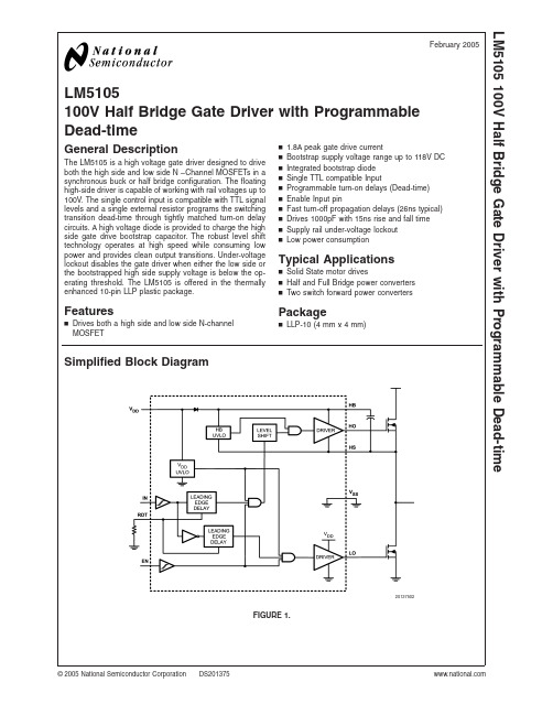
LM5105100V Half Bridge Gate Driver with Programmable Dead-timeGeneral DescriptionThe LM5105is a high voltage gate driver designed to drive both the high side and low side N –Channel MOSFETs in a synchronous buck or half bridge configuration.The floating high-side driver is capable of working with rail voltages up to 100V.The single control input is compatible with TTL signal levels and a single external resistor programs the switching transition dead-time through tightly matched turn-on delay circuits.A high voltage diode is provided to charge the high side gate drive bootstrap capacitor.The robust level shift technology operates at high speed while consuming low power and provides clean output transitions.Under-voltage lockout disables the gate driver when either the low side or the bootstrapped high side supply voltage is below the op-erating threshold.The LM5105is offered in the thermally enhanced 10-pin LLP plastic package.Featuresn Drives both a high side and low side N-channel MOSFETn 1.8A peak gate drive currentn Bootstrap supply voltage range up to 118V DC n Integrated bootstrap diode n Single TTL compatible Inputn Programmable turn-on delays (Dead-time)n Enable Input pinn Fast turn-off propagation delays (26ns typical)n Drives 1000pF with 15ns rise and fall time n Supply rail under-voltage lockout nLow power consumptionTypical Applicationsn Solid State motor drivesn Half and Full Bridge power converters n Two switch forward power convertersPackagen LLP-10(4mm x 4mm)Simplified Block Diagram20137502FIGURE 1.February 2005LM5105100V Half Bridge Gate Driver with Programmable Dead-time©2005National Semiconductor Corporation Connection Diagram2013750110-Lead LLPSee NS Number SDC10AOrdering InformationOrdering Number Package TypeNSC Package DrawingSupplied AsLM5105SD LLP-10SDC10A 1000shipped as Tape &Reel LM5105SDXLLP-10SDC10A4500shipped as Tape &ReelPin DescriptionsPin Name DescriptionApplication Information1V DD Positive gate drive supply Decouple VDD to VSS using a low ESR/ESL capacitor,placed as close to the IC as possible.2HBHigh side gate driver bootstrap rail Connect the positive terminal of bootstrap capacitor to the HB pin and connect negative terminal to HS.The Bootstrap capacitor should be placed as close to IC as possible.3HO High side gate driver outputConnect to the gate of high side N-MOS device through a short,low inductance path.4HS High side MOSFET source connection Connect to the negative terminal of the bootststrap capacitor and to the source of the high side N-MOS device.5NC Not Connected6RDTDeadtime programming pinA resistor from RDT to VSS programs the turn-on delay of both the high and low side MOSFETs.The resistor should be placed close to the IC to minimize noise coupling from adjacent PC board traces.7EN Logic input for driver Disable/EnableTTL compatible threshold with hysteresis.LO and HO are held in the low state when EN is low.8IN Logic input for gate driver TTL compatible threshold with hysteresis.The high side MOSFET is turned on and the low side MOSFET turned off when IN is high.9V SS Ground returnAll signals are referenced to this ground.10LOLow side gate driver outputConnect to the gate of the low side N-MOS device with a short,low inductance path.L M 5105 2Absolute Maximum Ratings(Note1)If Military/Aerospace specified devices are required, please contact the National Semiconductor Sales Office/ Distributors for availability and specifications.V DD to V SS–0.3V to+18VHB to HS–0.3V to+18VIN and EN to V SS–0.3V to V DD+0.3VLO to V SS–0.3V to V DD+0.3VHO to V SS HS–0.3V to HB+0.3VHS to V SS(Note6)−5V to+100VHB to V SS118VRDT to V SS–0.3V to5VJunction Temperature+150˚CStorage Temperature Range–55˚C to+150˚C ESD Rating HBM(Note2)2kVRecommended Operating ConditionsV DD+8V to+14V HS(Note6)–1V to100V HB HS+8V to HS+14V HS Slew Rate<50V/ns Junction Temperature–40˚C to+125˚CElectrical Characteristics Specifications in standard typeface are for TJ=+25˚C,and those in boldfacetype apply over the full operating junction temperature range.Unless otherwise specified,V DD=HB=12V,V SS=HS=0V,EN=5V.No load on LO or HO.RDT=100kΩ(Note4).Symbol Parameter Conditions Min Typ Max Units SUPPLY CURRENTSI DD V DD Quiescent Current IN=EN=0V0.340.6mAI DDO V DD Operating Current f=500kHz 1.653mAI HB Total HB Quiescent Current IN=EN=0V0.060.2mAI HBO Total HB Operating Current f=500kHz 1.33mAI HBS HB to V SS Current,Quiescent HS=HB=100V0.0510µAI HBSO HB to V SS Current,Operating f=500kHz0.1mAINPUT IN and ENV IL Low Level Input Voltage Threshold0.8 1.8VV IH High Level Input Voltage Threshold 1.8 2.2VR pd Input Pulldown Resistance Pin IN and EN100200500kΩDEAD-TIME CONTROLSVRDT Nominal Voltage at RDT 2.73 3.3VIRDT RDT Pin Current Limit RDT=0V0.75 1.5 2.25mA UNDER VOLTAGE PROTECTIONV DDR V DD Rising Threshold 6.0 6.97.4VV DDH V DD Threshold Hysteresis0.5VV HBR HB Rising Threshold 5.7 6.67.1VV HBH HB Threshold Hysteresis0.4VBOOT STRAP DIODEV DL Low-Current Forward Voltage I VDD-HB=100µA0.60.9VV DH High-Current Forward Voltage I VDD-HB=100mA0.85 1.1VR D Dynamic Resistance I VDD-HB=100mA0.8 1.5ΩLO GATE DRIVERV OLL Low-Level Output Voltage I LO=100mA0.250.4VV OHL High-Level Output Voltage I LO=–100mA,V OHL=V DD–V LO0.350.55VI OHL Peak Pullup Current LO=0V 1.8AI OLL Peak Pulldown Current LO=12V 1.6AHO GATE DRIVERV OLH Low-Level Output Voltage I HO=100mA0.250.4VV OHH High-Level Output Voltage I HO=–100mA,V OHH=HB–HO0.350.55VI OHH Peak Pullup Current HO=0V 1.8ALM51053Electrical Characteristics Specifications in standard typeface are for T J =+25˚C,and those in boldface typeapply over the full operating junction temperature range .Unless otherwise specified,V DD =HB =12V,V SS =HS =0V,EN =5V.No load on LO or HO.RDT=100k Ω(Note 4).(Continued)Symbol ParameterConditionsMinTyp MaxUnits I OLH Peak Pulldown CurrentHO =12V1.6ATHERMAL RESISTANCEθJAJunction to Ambient(Note 3),(Note 5)40˚C/WSwitching CharacteristicsSpecifications in standard typeface are for T J =+25˚C,and those in boldfacetype apply over the full operating junction temperature range .Unless otherwise specified,V DD =HB =12V,V SS =HS =0V,No Load on LO or HO (Note 4).Symbol ParameterConditionsMinTyp Max Units t LPHL Lower Turn-Off Propagation Delay 2656ns t HPHL Upper Turn-Off Propagation Delay 2656ns t LPLH Lower Turn-On Propagation Delay RDT =100k 485595705ns t HPLH Upper Turn-On Propagation Delay RDT =100k 485595705ns t LPLH Lower Turn-On Propagation Delay RDT =10k 75105150ns t HPLH Upper Turn-On Propagation Delay RDT =10k75105150ns t en ,t sd Enable and Shutdown propagation delay 28ns DT1,DT2Dead-time LO OFF to HO ON &HO OFF to LO ONRDT =100k 570µsRDT =10k 80MDT Dead-time matching RDT =100k 50t R ,t F Either Output Rise/Fall TimeC L =1000pF15t BSBootstrap Diode Turn-On or Turn-Off TimeI F =20mA,I R =200mA 50nsNote 1:Absolute Maximum Ratings indicate limits beyond which damage to the component may occur.Operating Ratings are conditions under which operation of the device is guaranteed.Operating Ratings do not imply guaranteed performance limits.For guaranteed performance limits and associated test conditions,see the Electrical Characteristics tables.Note 2:The human body model is a 100pF capacitor discharged through a 1.5k Ωresistor into each pin.Pin 2,Pin 3and Pin 4are rated at 500V.Note 3:4layer board with Cu finished thickness 1.5/1.0/1.0/1.5oz.Maximum die size used.5x body length of Cu trace on PCB top.50x 50mm ground and power planes embedded in PCB.See Application Note AN-1187.Note 4:Min and Max limits are 100%production tested at 25˚C.Limits over the operating temperature range are guaranteed through correlation using Statistical Quality Control (SQC)methods.Limits are used to calculate National’s Average Outgoing Quality Level (AOQL).Note 5:The θJA is not a constant for the package and depends on the printed circuit board design and the operating conditions.Note 6:In the application the HS node is clamped by the body diode of the external lower N-MOSFET,therefore the HS voltage will generally not exceed -1V.However in some applications,board resistance and inductance may result in the HS node exceeding this stated voltage transiently.If negative transients occur on HS,the HS voltage must never be more negative than V DD -15V.For example,if V DD =10V,the negative transients at HS must not exceed -5V.L M 5105 4Typical Performance CharacteristicsV DD Operating Current vs Frequency Operating Current vs Temperature2013751020137511 Quiescent Current vs Supply Voltage Quiescent Current vs Temperature2013751220137513 HB Operating Current vs Frequency HO&LO Peak Output Current vs Output Voltage2013751620137517LM51055Typical Performance Characteristics(Continued)Diode Forward VoltageUndervoltage Hysteresis vs Temperature2013751520137518Undervoltage Rising Threshold vs Temperature LO &HO -High Level Output Voltage vs Temperature2013751920137520LO &HO -Low Level Output Voltage vs Temperature Input Threshold vs Temperature2013752120137522L M 5105 6Typical Performance Characteristics(Continued)Dead-Time vs RT Resistor ValueDead-Time vs Temperature (RT =10k)2013751420137526Dead-Time vs Temperature (RT =100k)20137527LM51057Timing DiagramsOperational NotesThe LM5105is a single PWM input Gate Driver with Enable that offers a programmable deadtime.The deadtime is set with a resistor at the RDT pin and can be adjusted from 100ns to 600ns.The wide deadtime programming range provides the flexibility to optimize drive signal timing for a wide range of MOSFETS and applications.The RDT pin is biased at 3V and current limited to 1mA maximum programming current.The time delay generator will accommodate resistor values from 5k to 100k with a deadtime time that is proportional to the RDT resistance.Grounding the RDT pin programs the LM5105to drive both outputs with minimum deadtime.STARTUP AND UVLOBoth top and bottom drivers include under-voltage lockout (UVLO)protection circuitry which monitors the supply volt-age (V DD )and bootstrap capacitor voltage (HB –HS)inde-pendently.The UVLO circuit inhibits each driver until suffi-cient supply voltage is available to turn-on the external MOSFETs,and the UVLO hysteresis prevents chattering during supply voltage transitions.When the supply voltage is applied to the V DD pin of LM5105,the top and bottom gates are held low until V DD exceeds the UVLO threshold,typically about 6.9V.Any UVLO condition on the bootstrap capacitor will disable only the high side output (HO).20137503LM5105Input -Output WaveformsFIGURE 2.20137504LM5105Switching Time Definitions:t LPLH ,t LPHL ,t HPLH ,t HPHLFIGURE 3.20137530LM5105Enable:t sdFIGURE 4.20137531LM5105Dead-time:DTFIGURE 5.L M 5105 8Operational Notes(Continued)LAYOUT CONSIDERATIONSThe optimum performance of high and low side gate drivers cannot be achieved without taking due considerations during circuit board layout.Following points are emphasized.1.A low ESR/ESL capacitor must be connected close tothe IC,and between V DD and V SS pins and between HB and HS pins to support high peak currents being drawn from V DD during turn-on of the external MOSFET.2.To prevent large voltage transients at the drain of the topMOSFET,a low ESR electrolytic capacitor must be con-nected between MOSFET drain and ground(V SS).3.In order to avoid large negative transients on the switchnode(HS)pin,the parasitic inductances in the source of top MOSFET and in the drain of the bottom MOSFET (synchronous rectifier)must be minimized.4.Grounding considerations:a)The first priority in designing grounding connections isto confine the high peak currents from charging and discharging the MOSFET gate in a minimal physical area.This will decrease the loop inductance and mini-mize noise issues on the gate terminal of the MOSFET.The MOSFETs should be placed as close as possible to the gate driver.b)The second high current path includes the bootstrapcapacitor,the bootstrap diode,the local ground refer-enced bypass capacitor and low side MOSFET body diode.The bootstrap capacitor is recharged on the cycle-by-cycle basis through the bootstrap diode from the ground referenced V DD bypass capacitor.The re-charging occurs in a short time interval and involves high peak current.Minimizing this loop length and area on the circuit board is important to ensure reliable operation.5.The resistor on the RDT pin must be placed very close tothe IC and seperated from high current paths to avoid noise coupling to the time delay generator which could disrupt timer operation.POWER DISSIPATION CONSIDERATIONSThe total IC power dissipation is the sum of the gate driverlosses and the bootstrap diode losses.The gate driverlosses are related to the switching frequency(f),output loadcapacitance on LO and HO(C L),and supply voltage(V DD)and can be roughly calculated as:P DGATES=2•f•C L•V DD2There are some additional losses in the gate drivers due tothe internal CMOS stages used to buffer the LO and HOoutputs.The following plot shows the measured gate driverpower dissipation versus frequency and load capacitance.Athigher frequencies and load capacitance values,the powerdissipation is dominated by the power losses driving theoutput loads and agrees well with the above equation.Thisplot can be used to approximate the power losses due to thegate drivers.Gate Driver Power Dissipation(LO+HO)V CC=12V,Neglecting Diode Losses20137505 The bootstrap diode power loss is the sum of the forwardbias power loss that occurs while charging the bootstrapcapacitor and the reverse bias power loss that occurs duringreverse recovery.Since each of these events happens onceper cycle,the diode power loss is proportional to frequency.Larger capacitive loads require more current to recharge thebootstrap capacitor resulting in more losses.Higher inputvoltages(V IN)to the half bridge result in higher reverserecovery losses.The following plot was generated based oncalculations and lab measurements of the diode recoverytime and current under several operating conditions.Thiscan be useful for approximating the diode power dissipation.LM51059Operational Notes(Continued)Diode Power Dissipation V IN =80V20137506Diode Power Dissipation V IN =40V20137507The total IC power dissipation can be estimated from the above plots by summing the gate drive losses with the bootstrap diode losses for the intended application.Because the diode losses can be significant,an external diode placed in parallel with the internal bootstrap diode (refer to Figure 6)and can be helpful in removing power from the IC.For this to be effective,the external diode must be placed close to the IC to minimize series inductance and have a significantly lower forward voltage drop than the internal diode.HS Transient Voltages Below GroundThe HS node will always be clamped by the body diode of the lower external FET.In some situations,board resis-tances and inductances can cause the HS node to tran-siently swing several volts below ground.The HS node can swing below ground provided:1.HS must always be at a lower potential than HO.Pulling HO more than -0.3V below HS can activate parasitic transistors resulting in excessive current to flow from the HB supply possibly resulting in damage to the IC.The same relationship is true with LO and VSS.If necessary,a Schottky diode can be placed externally between HO and HS or LO and GND to protect the IC from this type of transient.The diode must be placed as close to the IC pins as possible in order to be effective.2.HB to HS operating voltage should be 15V or less .Hence,if the HS pin transient voltage is -5V,VDD should be ideally limited to 10V to keep HB to HS below 15V.3.A low ESR bypass capacitor between HB to HS as wellas VCC to VSS is essential for proper operation.The capacitor should be located at the leads of the IC to minimize series inductance.The peak currents from LO and HO can be quite large.Any series inductances with the bypass capacitor will cause voltage ringing at the leads of the IC which must be avoided for reliable op-eration.L M 5105 10LM5105 Operational Notes(Continued)LM5105Driving MOSFETs Connected in Half-Bridge Configuration Array20137508FIGURE6.11Physical Dimensionsinches (millimeters)unless otherwise notedNotes:Unless otherwise specified1.Standard lead finish to be 200microinches/5.00micrometers minimum tin/lead (solder)on copper.2.Pin 1identification to have half of full circle option.3.No JEDEC registration as of Feb.2000.LLP-10Outline Drawing NS Package Number SDC10ANational does not assume any responsibility for use of any circuitry described,no circuit patent licenses are implied and National reserves the right at any time without notice to change said circuitry and specifications.For the most current product information visit us at .LIFE SUPPORT POLICYNATIONAL’S PRODUCTS ARE NOT AUTHORIZED FOR USE AS CRITICAL COMPONENTS IN LIFE SUPPORT DEVICES OR SYSTEMS WITHOUT THE EXPRESS WRITTEN APPROVAL OF THE PRESIDENT AND GENERAL COUNSEL OF NATIONAL SEMICONDUCTOR CORPORATION.As used herein:1.Life support devices or systems are devices or systems which,(a)are intended for surgical implant into the body,or (b)support or sustain life,and whose failure to perform when properly used in accordance with instructions for use provided in the labeling,can be reasonably expected to result in a significant injury to the user.2.A critical component is any component of a life support device or system whose failure to perform can be reasonably expected to cause the failure of the life support device or system,or to affect its safety or effectiveness.BANNED SUBSTANCE COMPLIANCENational Semiconductor certifies that the products and packing materials meet the provisions of the Customer Products Stewardship Specification (CSP-9-111C2)and the Banned Substances and Materials of Interest Specification (CSP-9-111S2)and contain no ‘‘Banned Substances’’as defined in CSP-9-111S2.National Semiconductor Americas Customer Support CenterEmail:new.feedback@ Tel:1-800-272-9959National SemiconductorEurope Customer Support CenterFax:+49(0)180-5308586Email:europe.support@Deutsch Tel:+49(0)6995086208English Tel:+44(0)8702402171Français Tel:+33(0)141918790National Semiconductor Asia Pacific Customer Support CenterEmail:ap.support@National SemiconductorJapan Customer Support Center Fax:81-3-5639-7507Email:jpn.feedback@ Tel:81-3-5639-7560L M 5105100V H a l f B r i d g e G a t e D r i v e r w i t h P r o g r a m m a b l e D e a d -t i m e。
主流功放芯片参数及比较
低档运放JRC4558。
这种运放是低档机器使用得最多的。
现在被认为超级烂,因为它的声音过于明亮,毛刺感强,所以比起其他的音响用运放来说是最差劲的一种。
不过它在我国暂时应用得还是比较多的,很多的四、五百元的功放还是选择使用它,因为考虑到成本问题和实际能出的效果,没必要选择质量超过5532以上的运放。
对于一些电脑有源音箱来说,它的应付能力还是绰绰有余的。
运放之皇5532。
如果有谁还没有听说过它名字的话,那就还未称得上是音响爱好者。
这个当年有运放皇之称的NE5532,与LM833、LF353、CA3240一起是老牌四大名运放,不过现在只有5532应用得最多。
5532现在主要分开台湾、美国和PHILIPS生产的,日本也有。
5532原来是美国SIGNE公司的产品,所以质量最好的是带大S标志的美国产品,市面上要正宗的要卖8元以上,自从SIGNE被PHILIPS 收购后,生产的5532商标使用的都是PHILIPS商标,质量和原品相当,只须4-5元。
而台湾生产的质量就稍微差一些,价格也最便,两三块便可以买到了。
NE5532的封装和4558一样,都是DIP8脚双运放(功能引脚见图),声音特点总体来说属于温暖细腻型,驱动力强,但高音略显毛糙,低音偏肥。
以前不少人认为它有少许的“胆味”,不过现在比它更有胆味的已有不少,相对来说就显得不是那么突出了。
5532的电压适应范围非常宽,从正负3V至正负20V都能正常工作。
它虽然是一个比较旧的运放型号,但现在仍被认为是性价比最高的音响用运放。
是属于平民化的一种运放,被许多中底档的功放采用。
不过现在有太多的假冒NE5532,或非音频用的工业用品,由于5532的引脚功能和4558的相同,所以有些不良商家还把4558擦掉字母后印上5532字样充当5532,一般外观粗糙,印字易擦掉,有少许经验的人也可以辨别。
据说有8mA的电流温热才是正宗的音频用5532。
NE5532还有两位兄弟NE5534和NE5535。
供应商代码(采购部提供)20110314
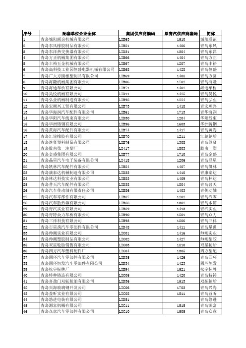
配套单位企业全称 青岛城阳联谊机械有限公司 青岛东风橡胶制品有限公司 青岛东洋热交换器有限公司 青岛方正机械集团有限公司 青岛丰裕五金机械有限公司 青岛高科技工业园恒盛电器机械有限公司 青岛广大方圆橡塑制品有限公司 青岛海隆机械集团有限公司 青岛海通车桥有限公司 青岛昊悦机械有限公司 青岛弘业机械制造有限公司 青岛宏顺兴工贸有限公司 青岛华海润汽车配件有限公司 青岛华阳汽车线束有限公司 青岛华洲铸钢有限公司 青岛黄海汽车配件有限公司 青岛汇轮橡胶有限公司 青岛继贤塑料制品有限公司 青岛胶南第一注塑厂 青岛金盛集团有限公司 青岛晶星汽车电子装备有限公司 青岛凯林汽车配件有限公司 青岛康泰达机械制造有限公司 青岛林达科技实业有限公司 青岛普天汽车配件有限公司 青岛汽车传动轴有限责任公司 青岛汽车零部件有限公司 青岛汽车散热器有限公司 青岛青汽实业有限公司 青岛青特众力车桥有限公司 青岛三祥科技有限公司 青岛市星禹汽车零部件有限公司 青岛帅潮实业有限公司 青岛帅潮塑胶制品有限公司 青岛双星轮胎销售有限公司 青岛四方汽车塑料配件厂 青岛四环汽车零部件有限公司 青岛四环旭发汽车零部件有限公司 青岛松宇标牌厂 青岛特种铸造有限公司 青岛喜盈门双驼轮胎有限公司 青岛兴海玻璃钢开发公司 青岛益昕实业有限公司 青岛悠进电装有限公司 青岛源富机械有限公司 青岛众意汽车零部件有限公司
山东德泰机械制造集团有限公司 LIC19 山东高强紧固件有限公司 LIC34 山东海达通汽车零部件有限公司 LID37 山东华龙机械有限公司 LIB25 山东济宁车轮厂 LIC22 山东玲珑轮胎股份有限公司 LIC24 山东龙口蓄电池总厂 LI506 山东鲁得贝车灯股份有限公司 LI103 山东鲁运机械配件有限公司 LID89 山东美晨科技股份有限公司 LIC26 山东明水汽车配件有限公司 LI206 山东蓬翔汽车有限公司 LW219 山东省潍北机械厂 LID43 山东水星博惠汽车部件股份有限公司 LI603 山东旭鑫机械股份有限公司 LIB32 山东只楚民营科技园股份有限公司汽车内饰件分公司 LI431 陕西法士特齿轮有限责任公司 LK008 上海底特精密紧固件有限公司 LFB25 上海干巷车镜实业有限公司 LFB30 上海里盛国际贸易有限公司 LFD23 上海三民汽车车业有限公司 LFC76 上海通达汽车洗涤器厂 LFB79 上海中欧汽车电器有限公司 LFB96 沈阳三浦汽车电子有限公司 LC109 舒兰市通用机械有限责任公司 LA219 四川柯世达汽车制动系统集团有限公司 LRB14 四川绵阳德鑫机械有限公司 LRB79 四平慧宇仪表电气有限公司 LA911 四平市方向机械有限公司 LA403 苏州上声电子有限公司 LLC25 苏州万隆汽车饰件有限公司 LLC28 台州恒丰汽车零部件有限公司 LM301 泰州长力树脂管有限公司 LL122 泰州苏中天线集团有限公司 LL124 天合富奥商用车转向器(长春)有限公司 LA498 天津静达合成材料有限公司 LED19 天津市轶超金属结构有限公司 LEB64 威伯科汽车控制系统(中国)有限公司 LF116 威海威嘉电气有限责任公司 LIC38 潍柴动力股份有限公司 LI704 潍坊青特车桥有限公司 LID44 潍坊万达汽车工具有限公司 LIC42 温州天球电器有限公司 LM405 无锡彩登电子有限公司 LL529 无锡市海江汽车部件有限公司 LLC66 无锡市巨龙塑化有限公司 LLC79 无锡市凯华减震器有限公司 LLE31
供应商代码(采购部提供)20110314
141 142 143 144 145 146 147 148 149 150 151 152 153 154 155 156 157 158 159 160 161 162 163 164 165 166 167 168 169 170 171 172 173 174 175 176 177 178 179 180 181 182 183 184 185 186 187
河北亿利橡塑集团有限公司 河南邦德电子电器有限公司 衡水宇信汽车零部件有限公司 湖北美标汽车制冷系统有限公司 湖北三环离合器有限公司 黄山市汽车电器股份公司 吉林东光瑞宝车灯有限责任公司 吉林恒昌科技股份有限公司 吉林吉轻阻尼材料有限责任公司 吉林龙山有机硅有限公司 吉林省宝迪汽车零部件制造有限责任公司 吉林省玉林商贸有限公司 吉林市龙山福思特汽车附件有限公司 吉林市汽车部件制造厂 即墨市国建纺织机械厂 即墨市即东汽车配件厂 江苏林慧汽配有限公司 江苏新泉汽车饰件有限公司 江阴圣世杰机械制造有限公司 江阴协统汽车附件有限公司 荆州久阳汽车零部件制造有限公司 莱州市光大工贸有限公司 莱州市金声汽车电器有限公司 廊坊同达汽车零部件有限公司 临海市江南滤清器有限公司 临朐弘泰汽车配件有限公司 临朐县大地汽车零部件有限公司 临沂市工业生产资料有限公司 龙口市龙口开发区新华橡塑制品厂 龙口通力汽车配件有限公司 南京奥联汽车电子电器有限公司 南京大桥传动轴有限公司 南洋汽摩集团有限公司 宁波联大塑料管件有限公司 宁波联华汽车部件有限公司 宁波帅特龙车辆部件有限公司 蓬莱博泰汽车底盘有限责任公司 蓬莱宏升汽车配件有限公司 齐鲁轮业有限公司 秦皇岛燕大汽车零部件制造有限公司 青州市东方汽车配件制造有限公司 全兴精工集团有限公司 泉州国胜汽车部件实业有限公司 瑞安市瑞强标准件有限公司 瑞安市云顶汽车冲压件有限公司 瑞立集团瑞安汽车零部件有限公司 沙市久隆汽车动力转向器有限公司
- 1、下载文档前请自行甄别文档内容的完整性,平台不提供额外的编辑、内容补充、找答案等附加服务。
- 2、"仅部分预览"的文档,不可在线预览部分如存在完整性等问题,可反馈申请退款(可完整预览的文档不适用该条件!)。
- 3、如文档侵犯您的权益,请联系客服反馈,我们会尽快为您处理(人工客服工作时间:9:00-18:30)。
LM5105100V Half Bridge Gate Driver with Programmable Dead-timeGeneral DescriptionThe LM5105is a high voltage gate driver designed to drive both the high side and low side N –Channel MOSFETs in a synchronous buck or half bridge configuration.The floating high-side driver is capable of working with rail voltages up to 100V.The single control input is compatible with TTL signal levels and a single external resistor programs the switching transition dead-time through tightly matched turn-on delay circuits.A high voltage diode is provided to charge the high side gate drive bootstrap capacitor.The robust level shift technology operates at high speed while consuming low power and provides clean output transitions.Under-voltage lockout disables the gate driver when either the low side or the bootstrapped high side supply voltage is below the op-erating threshold.The LM5105is offered in the thermally enhanced 10-pin LLP plastic package.Featuresn Drives both a high side and low side N-channel MOSFETn 1.8A peak gate drive currentn Bootstrap supply voltage range up to 118V DC n Integrated bootstrap diode n Single TTL compatible Inputn Programmable turn-on delays (Dead-time)n Enable Input pinn Fast turn-off propagation delays (26ns typical)n Drives 1000pF with 15ns rise and fall time n Supply rail under-voltage lockout nLow power consumptionTypical Applicationsn Solid State motor drivesn Half and Full Bridge power converters n Two switch forward power convertersPackagen LLP-10(4mm x 4mm)Simplified Block Diagram20137502FIGURE 1.February 2005LM5105100V Half Bridge Gate Driver with Programmable Dead-time©2005National Semiconductor Corporation Connection Diagram2013750110-Lead LLPSee NS Number SDC10AOrdering InformationOrdering Number Package TypeNSC Package DrawingSupplied AsLM5105SD LLP-10SDC10A 1000shipped as Tape &Reel LM5105SDXLLP-10SDC10A4500shipped as Tape &ReelPin DescriptionsPin Name DescriptionApplication Information1V DD Positive gate drive supply Decouple VDD to VSS using a low ESR/ESL capacitor,placed as close to the IC as possible.2HBHigh side gate driver bootstrap rail Connect the positive terminal of bootstrap capacitor to the HB pin and connect negative terminal to HS.The Bootstrap capacitor should be placed as close to IC as possible.3HO High side gate driver outputConnect to the gate of high side N-MOS device through a short,low inductance path.4HS High side MOSFET source connection Connect to the negative terminal of the bootststrap capacitor and to the source of the high side N-MOS device.5NC Not Connected6RDTDeadtime programming pinA resistor from RDT to VSS programs the turn-on delay of both the high and low side MOSFETs.The resistor should be placed close to the IC to minimize noise coupling from adjacent PC board traces.7EN Logic input for driver Disable/EnableTTL compatible threshold with hysteresis.LO and HO are held in the low state when EN is low.8IN Logic input for gate driver TTL compatible threshold with hysteresis.The high side MOSFET is turned on and the low side MOSFET turned off when IN is high.9V SS Ground returnAll signals are referenced to this ground.10LOLow side gate driver outputConnect to the gate of the low side N-MOS device with a short,low inductance path.L M 5105 2Absolute Maximum Ratings(Note1)If Military/Aerospace specified devices are required, please contact the National Semiconductor Sales Office/ Distributors for availability and specifications.V DD to V SS–0.3V to+18VHB to HS–0.3V to+18VIN and EN to V SS–0.3V to V DD+0.3VLO to V SS–0.3V to V DD+0.3VHO to V SS HS–0.3V to HB+0.3VHS to V SS(Note6)−5V to+100VHB to V SS118VRDT to V SS–0.3V to5VJunction Temperature+150˚CStorage Temperature Range–55˚C to+150˚C ESD Rating HBM(Note2)2kVRecommended Operating ConditionsV DD+8V to+14V HS(Note6)–1V to100V HB HS+8V to HS+14V HS Slew Rate<50V/ns Junction Temperature–40˚C to+125˚CElectrical Characteristics Specifications in standard typeface are for TJ=+25˚C,and those in boldfacetype apply over the full operating junction temperature range.Unless otherwise specified,V DD=HB=12V,V SS=HS=0V,EN=5V.No load on LO or HO.RDT=100kΩ(Note4).Symbol Parameter Conditions Min Typ Max Units SUPPLY CURRENTSI DD V DD Quiescent Current IN=EN=0V0.340.6mAI DDO V DD Operating Current f=500kHz 1.653mAI HB Total HB Quiescent Current IN=EN=0V0.060.2mAI HBO Total HB Operating Current f=500kHz 1.33mAI HBS HB to V SS Current,Quiescent HS=HB=100V0.0510µAI HBSO HB to V SS Current,Operating f=500kHz0.1mAINPUT IN and ENV IL Low Level Input Voltage Threshold0.8 1.8VV IH High Level Input Voltage Threshold 1.8 2.2VR pd Input Pulldown Resistance Pin IN and EN100200500kΩDEAD-TIME CONTROLSVRDT Nominal Voltage at RDT 2.73 3.3VIRDT RDT Pin Current Limit RDT=0V0.75 1.5 2.25mA UNDER VOLTAGE PROTECTIONV DDR V DD Rising Threshold 6.0 6.97.4VV DDH V DD Threshold Hysteresis0.5VV HBR HB Rising Threshold 5.7 6.67.1VV HBH HB Threshold Hysteresis0.4VBOOT STRAP DIODEV DL Low-Current Forward Voltage I VDD-HB=100µA0.60.9VV DH High-Current Forward Voltage I VDD-HB=100mA0.85 1.1VR D Dynamic Resistance I VDD-HB=100mA0.8 1.5ΩLO GATE DRIVERV OLL Low-Level Output Voltage I LO=100mA0.250.4VV OHL High-Level Output Voltage I LO=–100mA,V OHL=V DD–V LO0.350.55VI OHL Peak Pullup Current LO=0V 1.8AI OLL Peak Pulldown Current LO=12V 1.6AHO GATE DRIVERV OLH Low-Level Output Voltage I HO=100mA0.250.4VV OHH High-Level Output Voltage I HO=–100mA,V OHH=HB–HO0.350.55VI OHH Peak Pullup Current HO=0V 1.8ALM51053Electrical Characteristics Specifications in standard typeface are for T J =+25˚C,and those in boldface typeapply over the full operating junction temperature range .Unless otherwise specified,V DD =HB =12V,V SS =HS =0V,EN =5V.No load on LO or HO.RDT=100k Ω(Note 4).(Continued)Symbol ParameterConditionsMinTyp MaxUnits I OLH Peak Pulldown CurrentHO =12V1.6ATHERMAL RESISTANCEθJAJunction to Ambient(Note 3),(Note 5)40˚C/WSwitching CharacteristicsSpecifications in standard typeface are for T J =+25˚C,and those in boldfacetype apply over the full operating junction temperature range .Unless otherwise specified,V DD =HB =12V,V SS =HS =0V,No Load on LO or HO (Note 4).Symbol ParameterConditionsMinTyp Max Units t LPHL Lower Turn-Off Propagation Delay 2656ns t HPHL Upper Turn-Off Propagation Delay 2656ns t LPLH Lower Turn-On Propagation Delay RDT =100k 485595705ns t HPLH Upper Turn-On Propagation Delay RDT =100k 485595705ns t LPLH Lower Turn-On Propagation Delay RDT =10k 75105150ns t HPLH Upper Turn-On Propagation Delay RDT =10k75105150ns t en ,t sd Enable and Shutdown propagation delay 28ns DT1,DT2Dead-time LO OFF to HO ON &HO OFF to LO ONRDT =100k 570µsRDT =10k 80MDT Dead-time matching RDT =100k 50t R ,t F Either Output Rise/Fall TimeC L =1000pF15t BSBootstrap Diode Turn-On or Turn-Off TimeI F =20mA,I R =200mA 50nsNote 1:Absolute Maximum Ratings indicate limits beyond which damage to the component may occur.Operating Ratings are conditions under which operation of the device is guaranteed.Operating Ratings do not imply guaranteed performance limits.For guaranteed performance limits and associated test conditions,see the Electrical Characteristics tables.Note 2:The human body model is a 100pF capacitor discharged through a 1.5k Ωresistor into each pin.Pin 2,Pin 3and Pin 4are rated at 500V.Note 3:4layer board with Cu finished thickness 1.5/1.0/1.0/1.5oz.Maximum die size used.5x body length of Cu trace on PCB top.50x 50mm ground and power planes embedded in PCB.See Application Note AN-1187.Note 4:Min and Max limits are 100%production tested at 25˚C.Limits over the operating temperature range are guaranteed through correlation using Statistical Quality Control (SQC)methods.Limits are used to calculate National’s Average Outgoing Quality Level (AOQL).Note 5:The θJA is not a constant for the package and depends on the printed circuit board design and the operating conditions.Note 6:In the application the HS node is clamped by the body diode of the external lower N-MOSFET,therefore the HS voltage will generally not exceed -1V.However in some applications,board resistance and inductance may result in the HS node exceeding this stated voltage transiently.If negative transients occur on HS,the HS voltage must never be more negative than V DD -15V.For example,if V DD =10V,the negative transients at HS must not exceed -5V.L M 5105 4Typical Performance CharacteristicsV DD Operating Current vs Frequency Operating Current vs Temperature2013751020137511 Quiescent Current vs Supply Voltage Quiescent Current vs Temperature2013751220137513 HB Operating Current vs Frequency HO&LO Peak Output Current vs Output Voltage2013751620137517LM51055Typical Performance Characteristics(Continued)Diode Forward VoltageUndervoltage Hysteresis vs Temperature2013751520137518Undervoltage Rising Threshold vs Temperature LO &HO -High Level Output Voltage vs Temperature2013751920137520LO &HO -Low Level Output Voltage vs Temperature Input Threshold vs Temperature2013752120137522L M 5105 6Typical Performance Characteristics(Continued)Dead-Time vs RT Resistor ValueDead-Time vs Temperature (RT =10k)2013751420137526Dead-Time vs Temperature (RT =100k)20137527LM51057Timing DiagramsOperational NotesThe LM5105is a single PWM input Gate Driver with Enable that offers a programmable deadtime.The deadtime is set with a resistor at the RDT pin and can be adjusted from 100ns to 600ns.The wide deadtime programming range provides the flexibility to optimize drive signal timing for a wide range of MOSFETS and applications.The RDT pin is biased at 3V and current limited to 1mA maximum programming current.The time delay generator will accommodate resistor values from 5k to 100k with a deadtime time that is proportional to the RDT resistance.Grounding the RDT pin programs the LM5105to drive both outputs with minimum deadtime.STARTUP AND UVLOBoth top and bottom drivers include under-voltage lockout (UVLO)protection circuitry which monitors the supply volt-age (V DD )and bootstrap capacitor voltage (HB –HS)inde-pendently.The UVLO circuit inhibits each driver until suffi-cient supply voltage is available to turn-on the external MOSFETs,and the UVLO hysteresis prevents chattering during supply voltage transitions.When the supply voltage is applied to the V DD pin of LM5105,the top and bottom gates are held low until V DD exceeds the UVLO threshold,typically about 6.9V.Any UVLO condition on the bootstrap capacitor will disable only the high side output (HO).20137503LM5105Input -Output WaveformsFIGURE 2.20137504LM5105Switching Time Definitions:t LPLH ,t LPHL ,t HPLH ,t HPHLFIGURE 3.20137530LM5105Enable:t sdFIGURE 4.20137531LM5105Dead-time:DTFIGURE 5.L M 5105 8Operational Notes(Continued)LAYOUT CONSIDERATIONSThe optimum performance of high and low side gate drivers cannot be achieved without taking due considerations during circuit board layout.Following points are emphasized.1.A low ESR/ESL capacitor must be connected close tothe IC,and between V DD and V SS pins and between HB and HS pins to support high peak currents being drawn from V DD during turn-on of the external MOSFET.2.To prevent large voltage transients at the drain of the topMOSFET,a low ESR electrolytic capacitor must be con-nected between MOSFET drain and ground(V SS).3.In order to avoid large negative transients on the switchnode(HS)pin,the parasitic inductances in the source of top MOSFET and in the drain of the bottom MOSFET (synchronous rectifier)must be minimized.4.Grounding considerations:a)The first priority in designing grounding connections isto confine the high peak currents from charging and discharging the MOSFET gate in a minimal physical area.This will decrease the loop inductance and mini-mize noise issues on the gate terminal of the MOSFET.The MOSFETs should be placed as close as possible to the gate driver.b)The second high current path includes the bootstrapcapacitor,the bootstrap diode,the local ground refer-enced bypass capacitor and low side MOSFET body diode.The bootstrap capacitor is recharged on the cycle-by-cycle basis through the bootstrap diode from the ground referenced V DD bypass capacitor.The re-charging occurs in a short time interval and involves high peak current.Minimizing this loop length and area on the circuit board is important to ensure reliable operation.5.The resistor on the RDT pin must be placed very close tothe IC and seperated from high current paths to avoid noise coupling to the time delay generator which could disrupt timer operation.POWER DISSIPATION CONSIDERATIONSThe total IC power dissipation is the sum of the gate driverlosses and the bootstrap diode losses.The gate driverlosses are related to the switching frequency(f),output loadcapacitance on LO and HO(C L),and supply voltage(V DD)and can be roughly calculated as:P DGATES=2•f•C L•V DD2There are some additional losses in the gate drivers due tothe internal CMOS stages used to buffer the LO and HOoutputs.The following plot shows the measured gate driverpower dissipation versus frequency and load capacitance.Athigher frequencies and load capacitance values,the powerdissipation is dominated by the power losses driving theoutput loads and agrees well with the above equation.Thisplot can be used to approximate the power losses due to thegate drivers.Gate Driver Power Dissipation(LO+HO)V CC=12V,Neglecting Diode Losses20137505 The bootstrap diode power loss is the sum of the forwardbias power loss that occurs while charging the bootstrapcapacitor and the reverse bias power loss that occurs duringreverse recovery.Since each of these events happens onceper cycle,the diode power loss is proportional to frequency.Larger capacitive loads require more current to recharge thebootstrap capacitor resulting in more losses.Higher inputvoltages(V IN)to the half bridge result in higher reverserecovery losses.The following plot was generated based oncalculations and lab measurements of the diode recoverytime and current under several operating conditions.Thiscan be useful for approximating the diode power dissipation.LM51059Operational Notes(Continued)Diode Power Dissipation V IN =80V20137506Diode Power Dissipation V IN =40V20137507The total IC power dissipation can be estimated from the above plots by summing the gate drive losses with the bootstrap diode losses for the intended application.Because the diode losses can be significant,an external diode placed in parallel with the internal bootstrap diode (refer to Figure 6)and can be helpful in removing power from the IC.For this to be effective,the external diode must be placed close to the IC to minimize series inductance and have a significantly lower forward voltage drop than the internal diode.HS Transient Voltages Below GroundThe HS node will always be clamped by the body diode of the lower external FET.In some situations,board resis-tances and inductances can cause the HS node to tran-siently swing several volts below ground.The HS node can swing below ground provided:1.HS must always be at a lower potential than HO.Pulling HO more than -0.3V below HS can activate parasitic transistors resulting in excessive current to flow from the HB supply possibly resulting in damage to the IC.The same relationship is true with LO and VSS.If necessary,a Schottky diode can be placed externally between HO and HS or LO and GND to protect the IC from this type of transient.The diode must be placed as close to the IC pins as possible in order to be effective.2.HB to HS operating voltage should be 15V or less .Hence,if the HS pin transient voltage is -5V,VDD should be ideally limited to 10V to keep HB to HS below 15V.3.A low ESR bypass capacitor between HB to HS as wellas VCC to VSS is essential for proper operation.The capacitor should be located at the leads of the IC to minimize series inductance.The peak currents from LO and HO can be quite large.Any series inductances with the bypass capacitor will cause voltage ringing at the leads of the IC which must be avoided for reliable op-eration.L M 5105 10LM5105 Operational Notes(Continued)LM5105Driving MOSFETs Connected in Half-Bridge Configuration Array20137508FIGURE6.11Physical Dimensionsinches (millimeters)unless otherwise notedNotes:Unless otherwise specified1.Standard lead finish to be 200microinches/5.00micrometers minimum tin/lead (solder)on copper.2.Pin 1identification to have half of full circle option.3.No JEDEC registration as of Feb.2000.LLP-10Outline Drawing NS Package Number SDC10ANational does not assume any responsibility for use of any circuitry described,no circuit patent licenses are implied and National reserves the right at any time without notice to change said circuitry and specifications.For the most current product information visit us at .LIFE SUPPORT POLICYNATIONAL’S PRODUCTS ARE NOT AUTHORIZED FOR USE AS CRITICAL COMPONENTS IN LIFE SUPPORT DEVICES OR SYSTEMS WITHOUT THE EXPRESS WRITTEN APPROVAL OF THE PRESIDENT AND GENERAL COUNSEL OF NATIONAL SEMICONDUCTOR CORPORATION.As used herein:1.Life support devices or systems are devices or systems which,(a)are intended for surgical implant into the body,or (b)support or sustain life,and whose failure to perform when properly used in accordance with instructions for use provided in the labeling,can be reasonably expected to result in a significant injury to the user.2.A critical component is any component of a life support device or system whose failure to perform can be reasonably expected to cause the failure of the life support device or system,or to affect its safety or effectiveness.BANNED SUBSTANCE COMPLIANCENational Semiconductor certifies that the products and packing materials meet the provisions of the Customer Products Stewardship Specification (CSP-9-111C2)and the Banned Substances and Materials of Interest Specification (CSP-9-111S2)and contain no ‘‘Banned Substances’’as defined in CSP-9-111S2.National Semiconductor Americas Customer Support CenterEmail:new.feedback@ Tel:1-800-272-9959National SemiconductorEurope Customer Support CenterFax:+49(0)180-5308586Email:europe.support@Deutsch Tel:+49(0)6995086208English Tel:+44(0)8702402171Français Tel:+33(0)141918790National Semiconductor Asia Pacific Customer Support CenterEmail:ap.support@National SemiconductorJapan Customer Support Center Fax:81-3-5639-7507Email:jpn.feedback@ Tel:81-3-5639-7560L M 5105100V H a l f B r i d g e G a t e D r i v e r w i t h P r o g r a m m a b l e D e a d -t i m e。