EVAL-ADV7802EB1Z;中文规格书,Datasheet资料
EVAL-AD7951EDZ;EVAL-AD7678CB;EVAL-AD7679CBZ;中文规格书,Datasheet资料

Evaluation Board For AD761x,762x/AD763xAD764x/AD765x/AD766x/AD767x/AD795x Preliminary Technical Data EVAL-AD76XXCBRev.PrWInformation furnished by Analog Devices is believed to be accurate and reliable.However, no responsibility is assumed by Analog Devices for its use, nor for anyinfringements of patents or other rights of third parties that may result from its use. Specifications subject to change without notice. No license is granted by implication or otherwise under any patent or patent rights of Analog Devices. Trademarks and registered trademarks are the property of their respective owners.One Technology Way, P.O. Box 9106, Norwood, MA 02062-9106, U.S.A. Tel: Fax: 781.326.8703© 2009 Analog Devices, Inc. All rights reserved.FEATURESVersatile analog signal conditioning circuitryOn-board reference, clock oscillator and buffersBuffered 14, 16 (or 18) bit parallel outputsBuffered serial port interfaceIdeal for DSP and data acquisition card interfacesAnalog and digital prototyping areaEVAL-CONTROL-BOARD compatibilityPC software for control and data analysisGENERAL DESCRIPTIONThe EV AL-AD76XXCB is an evaluation board for the 48 lead AD761X, AD762X, AD763X, AD764X, AD765X, AD766X,AD767X and AD795X 14-bit, 16-bit and 18- bit PulSAR®analog to digital converter (ADC) family. These low power, successive approximation register (SAR) architecture ADCs (see ordering guide for product list ) offer very high performance with 100kSPS to 3MSPS throughput rate range with a flexible parallel or serial interface. The evaluation board is designed to demonstrate the ADC's performance and to provide an easy to understand interface for a variety of system applications. A full description of the AD761X, AD762X, AD763X, AD764X,AD765X, AD766X, AD767X and AD795X is available in the Analog Devices data sheets and should be consulted when utilizing this evaluation board.The converter installed is an LQFP however, the LFCSP can also be mounted.The evaluation board is ideal for use with either the Analog Devices EV AL-CONTROL-BRD2 or EV AL-CONTROL-BRD3 (EV AL-CONTROL-BRDX), or as a stand-alone system. The design offers the flexibility of applying external control signals and is capable of generating conversion results on parallel 14-bit, 16-bit or 18-bit wide buffered outputs.On-board components include a high precision band gap reference, (AD780, ADR431, or ADR435), reference buffers, a signal conditioning circuit with two op-amps and digital logic. The board interfaces to the EV AL-CONTROL-BRDX with a 96-pin DIN connector. A 40-pin IDC connector is used for parallel output, and test points are provided for the serial port. SMB connectors are provided for the low noise analog signal source, and for an externally generated CNVST (convert start input.The term AD76XX-48 is used in this document to represent all the 48 lead PulSAR ADCs listed in the ordering guide.VEEFigure 1.Functional Block Diagram /EVAL-AD76XXCBPreliminary Technical DataRev. PrW | Page 2 of 22TABLE OF CONTENTSOverview........................................................................................3 Conversion Control/ Master Clock............................................3 Analog Input.................................................................................3 Power Supplies and Grounding..................................................4 Using the Eval-AD762X/AD765X/AD766X/ AD767XCB as Stand-Alone...................................................................................4 Supplying Power for Stand-Alone use.......................................4 Evaluation Board Setting for Bipolar ADC InputConfigurations..............................................................................5 Schematics/PCB Layout...............................................................5 Running the EVAL AD76XXCB Software................................5 Hardware Setup............................................................................5 Software Installation.....................................................................5 Running the Software...................................................................5 Setup Screen...................................................................................5 DC Testing - Histogram...............................................................6 AC Testing......................................................................................6 Decimated AC Testing (Averaging)............................................6 Serial Programmabel Port (AD7610, AD7612, AD7631,AD7634, AD7951).........................................................................6 Ordering Information....................................................................21 Ordering Guide.. (21)LIST OF FIGURESFigure 1.Functional Block Diagram...............................................1 Figure 2. Schematic, Analog............................................................9 Figure 3. Schematic, Digital...........................................................10 Figure 4. Schematic, Power............................................................11 Figure 5. Top Side Silk-Screen.......................................................12 Figure 6. Top Layer.........................................................................12 Figure 7. Ground Layer..................................................................13 Figure 8. Shield Layer.....................................................................13 Figure 9. Bottom Side Layer..........................................................14 Figure 10. Bottom Side Silk-Screen..............................................14 Figure 11. Setup Screen..................................................................15 Figure 12. Histogram Screen.........................................................16 Figure 13. FFT Screen....................................................................17 Figure 14. Time-Domain Screen..................................................18 Figure 15. Decimated (Averaging) Screen..................................19 Figure 16. Serial Programmable Port (SPP) Demo Screen. (20)LIST OF TABLESTable 1. CNVST Generation, Analog Input Range ...................3 Table 2. Software Compatible Products.........................................5 Table 3. Jumper Description............................................................7 Table 4. S16 - Configuration Select Switch Description..............7 Table 5. S35 - Configuration Select Switch Description...............7 Table 6.Test Points.............................................................................8 Table 7. Bill of Materials for the Connectors (8)/Preliminary Technical DataEVAL-AD76XXCBRev. PrW | Page 3 of 22OVERVIEWFigure 1 shows a block diagram of the EV AL-AD76XXCB evaluation board. When used in stand-alone mode or inconjunction with the EV AL-CONTROL BRDX, the gate array, U10, provides the necessary control signals for conversion and buffers the ADC data. The evaluation board is a flexible design that enables the user to choose among many different board configurations, analog signal conditioning, reference, and different modes of conversion data.CONVERSION CONTROL/ MASTER CLOCKConversion start (CNVST ) controls the sample rate of the ADC and is the only input needed for conversion; all SAR timing is generated internally. CNVST is generated either by the gate array or externally via J3 (SMB) and setting JP22 in the external (EXT) position. The evaluation board is factory configured for the CNVST range shown in Table 1. Externally generated CNVST should have very low jitter and sharp edges for the maximum dynamic performance of the part. Since CNVST jitter usually results in poor SNR performance, it is recommended to use the on-board CNVST generation whenever possible.The master clock (MCLK) source for the gate array is generated from the DSP CLKOUT pin (buffered) when using the EV AL- CONTROL BRDX or form U12, the 40MHz local oscillator slectabel when using the accompanying software. The range for CNVST in Table 1 is a ratio generated from this master clock. In stand-alone mode, other clock frequencies can be used tochange the gate array generated CNVST by this ratio. However, other timings will be affected – namely the slave serial clock (SCLK) interface. In serial slave mode, SCLK = MCLK. While the ADC is converting, activity on the BUSY pin turns on the LED, D2. Additionally, the BUSY signal can be monitored test point TP1. Buffered conversion data (BD) is available at U10 on the output bus BD[0:15] on the 40-pin IDC connector P2, and on the 96-pin connector P3. When operating with the EV AL-CONTROL-BRDX, data is transferred using a 16 bit bus and corresponding word and byte modes selectable with the software. For the 18 bit converters two consecutive 16 bit words are read, however, the ADC data is still read into the gate array as 18 bits. Additionally, BD is updated on the falling edge of BBUSY on P3-C17, and on the rising edge of DBUSY on P2-33. When either parallel or serial reading mode of the ADC is used, data is available on this parallel bus.When using Serial Mode, serial data is available at T3, T4, T5, and T6 (SDOUT, SCLK, SYNC and RDERROR) and buffered serial data is output on TP17, TP18, and TP19 (SCLK, SYNC, and SDOUT). When using Slave Serial Mode, the external serial clock SCLK applied to the ADC is the MCLK, U12, frequency (40MHz). Refer to the device specific datasheet for full details of the interface modes.Table 1. CNVST Generation, Analog Input RangePart Res (bits) SampleRateAnalog Input Range Analog Input Type AD7610 16 250kSPS 0-5V, 0-10V, +/-5V, +/-10V SE AD7612 16 750kSPS 0-5V, 0-10V, +/-5V, +/-10V SEAD7621 16 3MSPS 0 to 2.5V Diff, Unipolar AD7622 16 2MSPS 0 to 2.5V Diff, Unipolar AD7623 16 1.33MSPS 0 to 2.5V Diff, Unipolar AD7631 16 250kSPS 0-5V, 0-10V, +/-5V, +/-10V Diff AD7634 16 670kSPS 0-5V, 0-10V, +/-5V, +/-10V DiffAD7641 18 2MSPS 0 to 2.5V Diff, Unipolar AD7643 18 1.25MSPS 0 to 2.5V Diff, Unipolar AD7650 16 571KSPS 0 to 2.5V SE, Unipolar AD7651 16 100KSPS 0 to 2.5V SE, Unipolar AD7652 16 500KSPS 0 to 2.5V SE, Unipolar AD7653 16 1MSPS 0 to 2.5V SE, Unipolar AD7654 16 500KSPS 0 to 5V 2-CH, SE Unipolar AD765516500KSPS0 to 5V4-CH, SE Unipolar AD7660 16 100KSPS 0 to 2.5V SE, Unipolar AD7661 16 100KSPS 0 to 2.5V SE, Unipolar AD7663 16 250KSPS +/-5V SE, Bipolar AD7664 16 571KSPS 0 to 2.5V SE, Unipolar AD7665 16 571KSPS +/-5V SE, Bipolar AD7666 16 500KSPS 0 to 2.5V SE, Unipolar AD7667 16 1MSPS 0 to 2.5V SE, Unipolar AD7671 16 1MSPS +/-5V SE, Bipolar AD7674 18 800KSPS 0 to 5V Diff, Unipolar AD7675 16 100KSPS +/-2.5V Diff, Unipolar AD7676 16 500KSPS +/-2.5V Diff, Unipolar AD7677 16 1MSPS +/-2.5V Diff, Unipolar AD7678 18 100KSPS 0 to 5V Diff, Unipolar AD7679 18 571KSPS 0 to 5V Diff, Unipolar AD7951 141MSPS 0-5V, 0-10V,+/-5V, +/-10VSEANALOG INPUTThe analog input amplifier circuitry U6 and U7 (see schematic - Figure 2) allows flexible configuration changes such as positive or negative gain, input range scaling, filtering, addition of a DC component, use of different op-amp and supplies depending on the ADC. The analog input amplifiers are set as unity gain buffers at the factory. The supplies are selectable with solder pads JP8 (VDRV+) and JP3 (VDRV-) and are set for the ±12V range. Table 1 shows the analog input range for the available evaluation boards.The default configuration for the single ended (SE) unipolar ADCs sets U6 at mid-scale from the voltage divider (V CM */EVAL-AD76XXCBPreliminary Technical DataRev. PrW | Page 4 of 22R6/(R6+R7)) and U7 at mid-scale from the voltage divider (V CM * R29(R29+R60)) for the differential unipolar ADCs.For the bipolar devices, the input is at 0V (mid-scale). This allows a transition noise test (histogram) without any other equipment. In some applications, it is desired to use a bipolar or wider analog input range, for instance, ± 10V , ± 5V , ± 2.5V , or 0 to -5V . For the AD76XX-48 parts which do not use these input ranges directly, simple modifications of the input drivercircuitry can be made without any performance degradation. Refer to the datasheet under the Application Hints section for component values or to application note AN594 on the product web page for other input ranges.For dynamic performance, an FFT test can be done by applying a very low distortion AC source.POWER SUPPLIES AND GROUNDINGThe evaluation board ground plane is separated into twosections: a plane for the digital interface circuitry and an analog plane for the analog input and external reference circuitry. To attain high resolution performance, the board was designed to ensure that all digital ground return paths do not cross the analog ground return paths by connecting the planes together directly under the converter. Power is supplied to the board through P3 when using with the EV AL-CONTROL-BRDXUSING THE EVAL-AD762X/AD765X/AD766X/ AD767XCB AS STAND-ALONEUsing the evaluation board as stand-alone does not require the EV AL-CONTROL-BRDX nor does it require use of theaccompanied software. When the CONTROL input to the gate array is LOW , which is pulled down by default, the gate array provides the necessary signals for conversion and buffers the conversion data.In stand-alone mode, the gate arrays flexible logic buffers the ADC data according to the read data mode configuration (word or byte). In parallel reading mode the board is configured for continuous reading since CS and RD are always driven LOW by the gate array. Thus, the digital bus is not tri-stated in this mode of operation and BD[0:15] will continuously be updated after a new conversion. BD[0:15] is available on P2 after BUSY goes HIGH. Note that with the 18 bit devices the full 18 bits of data BD[-2:15] are output directly on P2 since the evaluation board is not limited to 16 bit wide transfers in stand-alone operation. When either parallel or serial reading mode, the data is available on this parallel bus. Refer to Figure 2 to obtain the data output pins on P2.Configuration SwitchesThe evaluation board is configurable for the different operating modes with 16 positions on the configuration select switches, S16 and S35. A description of each switch setting and jumper position is listed in Table 4 and the available test points arelisted in Table 6. Note that the switches in the ON position define a logic HIGH level (pulled up with 10kΩ,) and that the switches are active only in stand-alone mode.For all interface modes, S16 and S35 allows the selection of: Warp, Normal or Impulse mode conversions (where applicable) Binary or 2s complement data output Reading during or after conversion Resetting the ADC ADC power-downInternal Reference and Buffer power-down (where applicable) In parallel reading mode, s16 allows the selection of: Byte swapping for 8 bit interfacing (LSByte with MSByte) 18-bit, 16-bit and 8-bit interfacing (for 18-bit converters) In serial reading mode, the default settings are Master Read during Conversion Mode using the internal ADC serial clock. Serial data is available at T3, T4, T5 and T6 for SDOUT, SCLK, SYNC and RDERROR respectively. Buffered serial data isoutput on the three test points TP17, TP18 and TP19 for SCLK, SYNC, and SDOUT respectively.For serial reading mode, S16 allows the selection of: Choice of inverting SCLK and SYNCChoice of using internal or external (slave mode) SCLKSUPPLYING POWER FOR STAND-ALONE USEPower needs to be supplied through the two power supplyblocks SJ1 and SJ2. Linear supplies are recommended. SJ1 is the analog supply for the ADC (AVDD), front end op amps and reference circuitry. SJ2 is the digital supply for the ADC(DVDD, OVDD) and gate array. The supplies to the device are configurable through the power supply jumpers shown in Figure 4 and/Preliminary Technical DataEVAL-AD76XXCBRev. PrW | Page 5 of 22Table 3. In most applications four supplies are required; ±12V and +5V for analog, and +5V for digital. On board regulators, where applicable, are used to reduce the operating voltages to the correct levels. The analog and digital supplies can be from the same source however, R27 (typically 20Ω) is required from AVDD to DVDD. In this configuration, JP9, DVDD selection, should be left open. Furthermore, the OVDD (ADC digital output supply) may need to be brought up after the analog +5V supply. See datasheet for details.EVALUATION BOARD SETTING FOR BIPOLAR ADC INPUT CONFIGURATIONSThe AD7610, AD7612, AD7631, AD7634, AD7663, AD7665, AD7671, and AD7951 can use both unipolar and bipolar ranges. The available options are +/-10V , +/-5V , +/-2.5V , 0 to 10V , 0 to 5V and 0 to 2.5V (depending on the ADC).For the AD7663, AD7665 and AD7671 the evaluation board is set for the ±5V bipolar input range since these ADCs inputranges are hardware pin strapped. Simple modifications to these evaluation boards can be made to accommodate the different input ranges by changing the INA-IND inputs with the available solder pads.iCMOS ADCsFor the AD7610, AD7612, AD7631 AD7634 and AD7951, the evaluation board can use all input ranges since the input range is controlled by software (or S16 DIP switches in stand-alone mode).For operating in unipolar mode for any of the bipolarevaluation boards it is recommended to use the voltage divider consisting of (V CM * R6/(R6+R7)) and (V CM * R29/(R29+R60)). This allows a transition noise test without any additional equipment.SCHEMATICS/PCB LAYOUTThe EV AL-AD76XXCB is a 4-layer board carefully laid out and tested to demonstrate the specific high accuracy performance of the AD76XX-48 device. Figure 2, Figure 3, and Figure 4, shows the schematics of the evaluation board. The printed circuitlayouts of the board are given in Figure 5 - Figure 10. Note these layouts are not to scale.Top side silk-screen - Figure 5 Top side layer - Figure 6 Ground layer - Figure 7 Shield layer - Figure 8Bottom side layer - Figure 9Bottom side silk-screen - Figure 10RUNNING THE EVAL AD76XXCB SOFTWAREThe evaluation board includes software for analyzing the AD761X, AD762X, AD763X, AD764X, AD765X, AD766X, AD767X, AD795X, AD67X and AD97x family. The EV AL-CONTROL-BRDX is required when using the software. Thesoftware is used to perform the following tests:• Histogram for determining code transition noise (DC) • Fast Fourier transforms (FFT) for signal to noise ratio (SNR), SNR and distortion (SINAD), total harmonicdistortion (THD) and spurious free dynamic range (SFDR) • Decimation (digital filtering)The evaluation software described in this document is also compatible with the following previous generation of high resolution ADCs.Table 2. Software Compatible ProductsEVAL AD676EB EVAL AD677EB EVAL AD974CB EVAL AD976CB EVAL AD976ACB EVAL AD977CB EVAL AD977ACBHARDWARE SETUPSystem Requirements• Evaluation Board• Evaluation Control Board 3 (or Board 2, not in production any longer)• AC Power Supply (AC 14V/1A source - can be purchased from ADI)• IEEE 1284 Compliant Parallel Port Cable (if not supplied) • DC source (low noise for checking different input ranges) • AC source (low distortion)• Bandpass filter suitable for 16 or 18 bit testing (value based on signal frequency)• PC operating Windows 2000 or XP .Connect the control board supplied mini plug to the 14V AC source. Connect the evaluation board to the controller board and connect the parallel port cable to the evaluation board and to the PC .SOFTWARE INSTALLATIONDouble-Click on setup.exe from the CD-ROM and follow the installation instructions. If upgrading the software, the previous version will first be removed. Thus setup.exe will need to be run again to install the new version. Reboot the computer.RUNNING THE SOFTWARETo run the software, use “Program Files”, “Analog Devices ADC” “ADC.exe”. The software has four screens as shown in Figure 11 through Figure 15. For the AD7610, AD7612, AD7631, AD7634 and AD7951, Figure 16 is a screen showing the Serial Programmable Port demonstration.SETUP SCREEN/EVAL-AD76XXCBPreliminary Technical DataRev. PrW | Page 6 of 22Figure 11 is the setup screen where ADC device selection, test type, input voltage range, sample rate and number of samples are selected.DC TESTING - HISTOGRAMFigure 12 is the histogram screen, which tests the codedistribution for DC input and computes the mean and standard deviation or transition noise. To perform a histogram test, select “Histogram” from the test selection window and click on the “Start” radio button. Note: a histogram test can be performed without an external source since the evaluation board has a buffered V REF /2 source at the ADC input for unipolar parts and at 0V for bipolar devices. To test other DC values, apply a source to the J1/J2 inputs. It is advised to filter the signal to make the DC source noise compatible with that of the ADC. C26/C41 provide this filtering.AC TESTINGFigure 13 is the FFT screen, which performs an FFT on the captured data and computes the SNR, SINAD, THD and SFDR. Figure 14 is the time domain representation of the output. To perform an AC test, apply a sinusoidal signal to the evaluation board at the SMB inputs J1 for IN+ and J2 for IN-. Low distortion, better than 100dB, is required to allow trueevaluation of the part. One possibility is to filter the input signal from the AC source. There is no suggested bandpass filter but consideration should be taken in the choice. Furthermore, if using a low frequency bandpass filter when the full-scale input range is more than a few Vpp, it is recommended to use the on board amplifiers to amplify the signal, thus preventing the filter from distorting the input signal.DECIMATED AC TESTING (AVERAGING)The AC performances can be evaluated after digital filtering with enhanced resolution of up to 32 bits. Figure 15 is the FFT screen when decimation is used. Additional bits of resolution are attained when over sampling by:SAMPLE N OVERSAMPLEf *f 4=where , N = number of bits and 4N .= the DRATIO. Set the DRATIO to the amount of over sampling desired. When using decimation, the test duration increases with the larger number of samples taken. The decimated test requires the EVAL-CONTROL-BRD3.SERIAL PROGRAMMABEL PORT (AD7610, AD7612, AD7631, AD7634, AD7951)Figure 16 is a screen showing the flexible serial programmable port (SPP) used on the AD7610, AD7612, AD7631, AD7634 and AD7951 i CMOS ADCs. The SPP can be used in any serial mode and allows the configuration of: unipolar and bipolar input ranges, mode selection, straight binary or 2’s complementoutput coding, and power down. The software demo allows two different configurations and alternates between these two every ten samples. To use just one range or mode, simply enter the same values into both “A ” and “B” configuration windows. Note that when using the unipolar input ranges, a common mode voltage must be provided externally (DC coupled) as the board is configured with the common mode = 0V/Preliminary Technical DataEVAL-AD76XXCBRev. PrW | Page 7 of 22Table 3. Jumper DescriptionJumper N ame DefaultPosition FunctionJP1, JP2BUFFBUFFBuffer amplifier: BUFF = use op amps to buffer analog input. NO BUFF = direct input from J1, J2 (SMB).J P3 VDRV- -12V Buffer amplifier negative supply: Selection of -12V, -5V or GND when using EVAL-CONTROL-BRDX or voltages on SJ1 in stand alone mode.JP4 REFS REF Reference selection: REF = use on board reference output for ADC reference. VDD = use analogsupply (AVDD) for ADC reference.J P6 OVDD 3.3V ADC digital output supply voltage: Selction of 2.5V, 3.3V and VDIG. VDIG = +5V when usingEVAL-CONTROL-BRDX or voltage on SJ2 in stand-alone mode.J P7 VREF+ +12V Reference circuit positive supply: Selection of +12V, +5V or AVDD when using EVAL-CONTROL-BRDX or voltages on SJ1 in stand alone mode.J P8 VDRV+ +12V Buffer amplifier positive supply: Selection of +12V, +5V or AVDD when using EVAL-CONTROL-BRDX or voltages on SJ1 in stand alone mode.J P9 DVDD VDIG/2.51 ADC digital supply voltage: Selection of +2.5V or VDIG (+5V) when using EVAL-CONTROL-BRDXor voltage on SJ2 in stand-alone mode. J P19 AVDD +5V/2.51ADC analog supply voltage: Selection of +2.5V, +5V or EXT when using EVAL-CONTROL-BRDX J P20 REFB BUF Reference buffer: BUFF = use U2 to buffer or amplify reference source. NO BUFF = use referencedirectly into ADC.J P21 VIO 3.3V Gate array I/O voltage: Selection of 3.3V or OVDD. Note: gate array will be damaged if >3.3V (ie.when using OVDD = VDIG).JP22 CNVST INT CNVST source: INT = use gate array to generate CNVST . EXT = use external source into J3, SMBfor CNVST .1For AD7621/AD7641 these are set to +2.5V. Note that setting these to +5V will permanently destruct the ADC.Table 4. S16 - Configuration Select Switch Description Note: (OFF = LOW , ON = HIGH)Position N ameDefault PositionFunction 1 WARP LOW Conversion mode selection: Used in conjunction with IMPULSE. When HIGH with IMPULSE=LOW, the fastest (Warp) mode is used for maximum throughput. When LOW and IMPULSE = LOW, Normal mode is used.2 IMPULSE LOW Conversion mode selection: Used in conjunction with WARP. When HIGH with WARP = LOW, areduced power mode is used in which the power consumption is proportional to the throughput rate.3 BIP LOW For future use.4 TEN LOW For future use.5 A0/M0 LOW A0, input Mux selection: Used for AD7654/AD7655 (refer to datasheet).M0, data output interface selection: Used along with M1 for 18-bit ADCs.6 BYTE/M1 LOW BYTESWAP, used for 8-bit interface mode on 16-bit ADCs: MSByte is swapped with LSByte on 8data lines.M1, data output interface selection: Used along with M0 for 18-bit ADCs.7 OB/2CHIGH Data output select: LOW = Use 2’s complement output. HIGH = Straight binary output. 8 SER/PARLOW Data output interface select: LOW = Parallel interface. HIGH = Serial interface. 9 EXT/INTLOW Serial clock source select: LOW = Use ADC internal serial clock, SCLK is an output. HIGH= Use external clock, which is MCLK (40 MHz) and SCLK is an input. Not used in parallel reading mode.10 INVSYNC LOW Serial sync (SYNC) active state: LOW = SYNC is active HIGH. HIGH = SYNC is active LOW. Usedonly for Master mode (internal SCLK). Not used in parallel reading mode.11 INVSCLK LOW Serial clock (SCLK) active edge: LOW = Use SCLK falling edge. HIGH = Use SCLK rising edge.Active in all serial modes. Not used in parallel reading mode.12 RDC LOW Read during convert: LOW = Read data after conversion (BUSY = LOW). HIGH = Read dataduring conversions (BUSY = HIGH). Used in both parallel and serial interface modes. Table 5. S35 - Configuration Select Switch Description Note: (OFF = LOW , ON = HIGH)/EVAL-AD76XXCBPreliminary Technical DataRev. PrW | Page 8 of 22Position N ameDefault PositionFunction1 RESET LOW Reset ADC: LOW = Enables the converter. HIGH = Abort conversion (if any).2 PD LOW Power down: LOW = Enables the converter . HIGH = Powers down the converter. Powerconsumption is reduced to a minimum after the current conversion.3 PDBUF LOW Internal reference buffer power down: LOW = Enable on chip buffer. HIGH = Power downinternal buffer.4 PDREF LOW Internal reference power down: LOW = Enable on chip reference. HIGH = Power down internalreference. Note that when using the on chip reference, the buffer also needs to be enabled (PDREF = PDBUF = HIGH).Table 6.Test PointsTest Point Available Signal Type Description TP1 BUSY Output BUSY signal.TP2 A0/M0 Input Same as S16, position 5 TP3 SIG+ Input Analog +input.TP4 AGND GNDAnalog ground close to SIG+.TP5 REF Input/Output Reference input. Output for devices with on-chip reference. TP7 DGND GND Digital ground near SJ2. TP8 CNVST Input CNVST signal.TP9 AGND GND Analog ground close to REF. TP10 CS Input CS , chip select signal. TP11 RD Input RD , read signal.TP12 OVDD Power Digital output supply. TP13 DVDD Power Digital core supply. TP14 AVDD Power Analog supply.TP15 AGND GND Analog ground close to SIG-.TP16 SIG- InputAnalog –input for differential parts. TP17 SCLK Input/Output Buffered serial clock. TP18 SYNC Output Buffered serial sync. TP19 SDOUT Output Buffered serial data.TP20TEMPOutputTEMP, for ADC with internal reference. Outputs temperature dependant voltage (approx. 300mV with T A = 25°C).TP22 REFINInput/Ouput For ADCs with internal reference, REFBUFIN can be used to connect external reference intothe reference buffer input when PDBUF = LOW and PDREF = HIGH. With the internalreference (and buffer) enabled, this pin will produce the intenal bandgap refrence voltage.TP23 BVDDOutput Internal reference bandgap supply. Connected to AVDD via s19. T3 SDOUT Output Direct ADC serial data. T4 SCLK Input/Output Direct ADC serial clock. T5 SYNC Output Direct ADC serial SYNC. T6 RDERROROutput Direct ADC serial read error.Table 7. Bill of Materials for the ConnectorsRef Des Connector Type Manf. Part No. J1 – J3 RT Angle SMB MalePasternack PE4177P2 0.100 X 0.100 straight IDC header 2X20 3M 2540-6002UB P332X3 RT PC MOUNT CONNECTORERNI533402/。
维亚维解决方案 OneAdvisor 800 产品数据表说明书
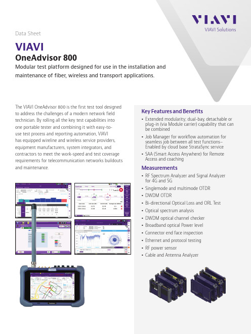
VIAVI
OneAdvisor 800
Modular test platform designed for use in the installation and maintenance of fiber, wireless and transport applications.
Size and weight (Mainframe)
Weight2ຫໍສະໝຸດ 0 kg (4.4 lb) without module (including battery)
Size (W x H x D)
270 x 170 x 60 mm (10.6 x 6.7 x 2.3 in) without module
ONA-800A-MF2G-T
OneAdvisor ONA-800A Mainframe with Display - no WiFi and Bluetooth Radios
Solution Hardware Modules
E81FMC1
Fiber module receptacle for E8100-series fiber modules
C2K-EMPTYMOD
Empty module to cover an unused expansion port
ONA-800A-DISPL ONA-800A-DISP-F ONA-800A-DISP-T
OneAdvisor Display
ONA-PMVFL
Power Meter and VFL Mainframe Module for OneAdvisor 800
AC Power with battery charging Battery discharging condition
W7802ABBD中文资料

(1
4.~ .08) 4.46 (113.22) 0.22 (5.5 N I P)
i
(2.0) ,
I
(4
0.06 )
I I'
SECTION A-A
(4x) 714.40 UN' 7MRU~
I ~ yI I 250)ip.~ ~ (0.67) A
I
I
I
I
I \ (4x) R 0.10 (250) `
a76(9s~)
W7800-Type 20 nm Thin-Film, Coarse Wavelength-Division Multiplexers and Demultiplexers
AdLib OCR Evaluation
Advance Data Sheet February 2002
Absolute Maximum Ratings
(2x) 1 .10
(2&00)
(4x) R 0.79 (20.00) (4x) R 0.73 (18.50)
'.0 N --
--H
I
-
B
(aao) 0 .63 (16.00)
0.12
I ~~ 0.47 I~T(1200)
\
- DELPoN
a9a 4. O6
4.62 (117.44)
/
EVAL-ADG788EBZ;中文规格书,Datasheet资料

Evaluation Board for ADG788Triple SPDT Switch in Chip Scale PackageEVAL-ADG788EBZ Rev. 0Evaluation boards are only intended for device evaluation and not for production purposes.Evaluation boards are supplied “as is” and without warranties of any kind, express, implied, orstatutory including, but not limited to, any implied warranty of merchantability or fitness for aparticular purpose. No license is granted by implication or otherwise under any patents or otherintellectual property by application or use of evaluation boards. Information furnished by AnalogDevices is believed to be accurate and reliable. However, no responsibility is assumed by AnalogDevices for its use, nor for any infringements of patents or other rights of third parties that may result from its use. Analog Devices reserves the right to change devices or specifications at any time without notice. T rademarks and registered trademarks are the property of their respective owners. Evaluation boards are not authorized to be used in life support devices or systems. One Technology Way, P.O. Box 9106, Norwood, MA 02062-9106, U.S.A. Tel: 781.329.4700 Fax: 781.461.3113 ©2007 Analog Devices, Inc. All rights reserved.FEATURESSupply voltageSingle: 1.8 V to 5.5 VDual: ±2.5 VTTL-/CMOS-compatible control inputsSwitch control optionsOn-board linksExternal control signalsRoHS compliantGENERAL DESCRIPTIONThis data sheet describes the evaluation board for the ADG788, a triple SPDT switch packaged in a compact 4 mm × 4 mm body, 20-lead LFCSP package. The switches are designed using an enhanced submicron CMOS process to provide optimal performance in terms of on resistance, bandwidth, and power dissipation. The excellent on resistance flatness makes the ADG788 ideal for a wide range of applications, including data and audio-video switching. Each SPDT switch can be individually controlled using a 1-wire parallel interface.The evaluation board supports both single- and dual-supply operation and comes fitted with connectors that allow the user to evaluate the performance of the ADG788 with minimum effort. The operation of the switches is controlled using the on-board links or by applying external control signals to the appropriate connectors.The data sheet for the ADG788 device is available from Analog Devices, Inc. It contains all the information regarding operation of the device, and it should be consulted in conjunction with this data sheet when using the evaluation board. EVALUATION BOARD6756-1 Figure 1.EVAL-ADG788EBZRev. 0 | Page 2 of 8TABLE OF CONTENTSFeatures..............................................................................................1 General Description.........................................................................1 Evaluation Board..............................................................................1 Revision History...............................................................................2 Evaluation Board Hardware............................................................3 Power Supply.................................................................................3 Switch Control..............................................................................3 Connections and Test Points.......................................................4 Evaluation Board Schematics and Artwork...................................5 Ordering Information.......................................................................7 Bill of Materials..............................................................................7 Ordering Guide.............................................................................7 ESD Caution.. (7)REVISION HISTORY6/07—Revision 0: Initial VersionEVAL-ADG788EBZRev. 0 | Page 3 of 8EVALUATION BOARD HARDWAREThe ADG788 evaluation board kit contains the following: •A fully fitted printed circuit board•A CD containing the ADG788 product data sheet and the evaluation board data sheetThe evaluation board allows the user to connect the signals that require switching to the ADG788 switch and control its operation by using the on-board links or by applying the correct control signals to the appropriate connectors. The signals present at the pins of the ADG788 can be monitored using the test point provided on the board.The following sections describe the function of all connectors and links.POWER SUPPLYTo operate the ADG788 evaluation board, the user must provide an external power supply connected to Power Block P1. The supply voltage range is 1.8 V to 5.5 V for single-supply operation and ±2.5 V for dual-supply operation. The user can select single-supply operation or dual-supply operation using Link J23, as shown in Table 1.Table 1. Link J23 ConfigurationP osition Operation Mode A Single-supply operation B Dual-supply operation (default configuration)SWITCH CONTROLThe four input pins, IN1, IN2, IN3, and IN4, control the opera-tion of the ADG788. Link J8, Link J9, Link J12, and Link J13 control the logic levels applied to these pins and allow the user to drive these pins with external signals applied to Connector J5 and Connector J11 (the signals have 50 Ω on-board termination resistors to GND). Table 2 describes the configuration achieved for each position of these links.Table 2. Link J8, Link J9, Link J12, and Link J13 SettingsLink Position ADG788 Switch StatusRemoved S2A to D2 = off, S2B to D2 = on AS2A to D2 = on, S2B to D2 = offHigh: S2A to D2 = on, S2B to D2 = off J8B (default configuration) Controlled via signal applied to Connector J5_TOP Low: S2A to D2 = off, S2B to D2 = onRemoved S3A to D3 = off, S3B to D3 = on AS3A to D3 = on, S3B to D3 = offHigh: S3A to D3 = on, S3B to D3 = off J9B (default configuration) Controlled via signal applied to Connector J5_BOTTOM Low: S3A to D3 = off, S3B to D3 = on RemovedS1A to D1 = off, S1B to D1 = onHigh: S1A to D1 = on, S1B to D1 = off A (default configuration) Controlled via signal applied to Connector J11_BOTTOM Low: S1A to D1 = off, S1B to D1 = onJ12BS1A to D1 = on, S1B to D1 = off RemovedS4A to D4 = off, S4B to D4 = onHigh: S4A to D4 = on, S4B to D4 = off A (default configuration) Controlled via signal applied to Connector J11_TOP Low: S4A to D4 = off, S4B to D4 = onJ13BS4A to D4 = on, S4B to D4 = offEVAL-ADG788EBZRev. 0 | Page 4 of 8CONNECTIONS AND TEST POINTSTable 3.Connector Position Test Point Connection to ADG788 Pin J1 Top T19 S1A Bottom T1 D1 J2 Top T2 S1B Bottom T3 S2B J3 Top T4 D2 Bottom T5 S2A J4 V DD T9 V DD GND T10 GND V SS T8 V SS J51Top T6 IN2 Bottom T7 IN3 J6 Top T11 S3A Bottom T12 D3 J7 Top T13 S3B Bottom T14 S4B J10 Top T15 D4 Bottom T16 S4A J111Top T17 IN4 Bottom T18 IN11This connector is tied to the ADG788 pins only when Link J8 and Link J9 are set in Position B, and J12 and J13 are in Position A.EVAL-ADG788EBZ EVALUATION BOARD SCHEMATICS AND ARTWORKFigure 2. Evaluation Board SchematicRev. 0 | Page 5 of 8EVAL-ADG788EBZRev. 0 | Page 6 of 806756-00306756-004Figure 3. Component Side PCB Drawing (Layer 1)Figure 4. Solder Side PCB Drawing (Layer2) Component Side ViewFigure 5. Component Side Silkscreen PCB DrawingEVAL-ADG788EBZRev. 0 | Page 7 of 8ORDERING INFORMATIONBILL OF MATERIALSTable 4.Qty Reference Designator DescriptionSupplier/Number 2 C1, C2 0.1 μF SMD ceramic capacitorFEC 301-9482 2 C3, C4 10 μF (0805 package) 10 V X5R SMD ceramic capacitor FEC 498-737 8 J1, J2, J3, J5, J6, J7, J10, J11 Dual phono connector FEC 128-0670 1 J4 3-pin power blockFEC 963-29805 J8, J9, J12, J13, J23 3-pin SIL header and shorting link FEC 486-1220 and FEC 148-029 4 R1, R2, R5, R6 10 kΩ SMD resistor FEC 933-0399 4 R3, R4, R7, R8 50 Ω SMD resistor FEC 933-1336 19 T1 to T19 Test point FEC 873-11281 U1ADG788BCPZ Analog Devices, Inc.ORDERING GUIDEModel P ackage DescriptionEVAL-ADG788EBZ 1ADG788 Evaluation Board1Z = RoHS Compliant Part.ESD CAUTIONEVAL-ADG788EBZRev. 0 | Page 8 of 8NOTES©2007 Analog Devices, Inc. All rights reserved. Trademarks and registered trademarks are the property of their respective owners.EB06756-0-6/07(0)分销商库存信息: ANALOG-DEVICES EVAL-ADG788EBZ。
广州唯创电子 WTB 系列语音芯片说明书
WTB系列语音芯片使用说明书目录1、WTB芯片特征 (3)2、应用范围 (3)3、WTB系列语音芯片选型 (3)4、WTB系列语音芯片应用方框图 (4)5、封装示意图 (4)6、管脚描述 (5)6.1、WTB015/031-16P封装引脚对应表 (5)6.2、WTB015-18S封装引脚对应表 (5)6.3、WTB031-18S封装引脚对应表 (6)6.4、WTB084-20SS/20P封装引脚对应表 (7)7、电器参数 (8)8、环境绝对极限参数 (8)9、定义IO口 (9)10、控制模式 (9)10.1、按键控制模式 (9)10.1.1、脉冲可重复触发 (9)10.1.2、脉冲不可重复触发 (9)10.1.3、电平保持可循环触发 (10)10.1.4、电平保持不可循环触发 (10)10.1.5、下一曲触发 (10)10.1.6、上一曲触发 (10)10.1.7、播放/停止触发 (11)10.1.8、播放/暂停触发 (11)10.2、一线串口控制模式 (11)10.2.1、端口分配表 (11)10.2.2、发送8位数据控制形式语音地址对应关系 (12)10.2.3、发送8位数据控制形式控制时序图 (12)10.2.4、发送16位数据控制形式语音地址对应关系 (12)10.2.5、发送16位数据控制形式控制时序图 (13)10.3、三线串口控制模式 (13)10.3.1、端口分配方式 (13)10.3.2、语音地址对应关系 (13)10.3.3、三线串口控制时序 (14)11、典型应用电路 (14)11.1、WTB015/031-16P (14)11.1.1、WTB015/031-16P按键控制(PWM输出)应用电路 (14)11.1.2、WTB015/031-16P按键控制(DAC输出)应用电路 (15)11.1.3、WTB015/031-16P一线串口控制(PWM输出)应用电路 (15)11.1.4、WTB015/031-16P一线串口控制(DAC输出)应用电路 (15)11.1.5、WTB015/031-16P三线串口控制(PWM输出)应用电路 (16)11.1.6、WTB015/031-16P三线串口控制(DAC输出)应用电路 (16)11.2、WTB015/031-18S (16)11.2.1、WTB015/031-18S按键控制(PWM输出)应用电路 (16)11.2.2、WTB031-18S按键控制(DAC输出)应用电路 (17)11.2.3、WTB015/031-18S一线串口控制(PWM输出)应用电路 (17)11.2.4、WTB015/031-18S一线串口控制(DAC输出)应用电路 (17)11.2.5、WTB015/031-18S三线串口(PWM输出)应用电路 (18)11.2.6、WTB015/031-18S三线串口(DAC输出)应用电路 (18)11.3、WTB084-20SS/20P (19)11.3.1、WTB084-20SS/20P按键控制(PWM输出)应用电路 (19)11.3.2、WTB084-20SS/20P按键控制(DAC输出)应用电路 (19)11.3.3、WTB084-20SS/20P一线串口(PWM输出)应用电路 (19)11.3.4、WTB084-20SS/20P一线串口(DAC输出)应用电路 (20)11.3.5、WTB084-20SS/20P三线串口(PWM输出)应用电路 (20)11.3.6、WTB084-20SS/20P三线串口(DAC输出)应用电路 (20)12、应用范例电路 (21)12.1、电动车应用电路 (21)12.2、定时药盒应用电路 (22)13、控制程序范例 (22)13.1、一线串口(发送8位数据控制形式)控制程序范例 (22)13.2、一线串口(发送16位数据控制形式)控制程序范例 (24)13.3、三线串口控制程序范例 (27)14、封装尺寸 (29)14.1、WTB015/031-16P封装尺寸 (29)14.2、WTB015/031-18S封装尺寸 (30)15、货源信息 (31)16、说明书版本记录 (31)1、WTB芯片特征WTB语音芯片是一款低成本OTP语音芯片;工业级性能,确保产品在多种场合下正常工作;内置音频合成器的4位微型语音处理器及4位数字逻辑运算器;WTB语音芯片完备的内部资源包括EPROM、RAM和I/O端口等;可定义多路输入端和输出端;随意定义控制输入端触发功能;自动休眠功能,有效降低功耗;支持WAV音频和两通道MIDI播放;可工作于4MHz和8MHz两种震荡模式,不同模式下的音频最高采样率分别为14KHz和28KHz;WTB系列语音芯片包括WTB015、WTB031、WTB084、WTB170,其存储时间分别为15秒、31秒、84秒、170秒,目前库存有WTB015、WTB031和WTB084三种;可加载128段语音进行控制播放;单芯片方案,可掩膜投产,降低批量生产成本;支持9bit D/A和8bit PWM输出;工作电压:DC2.2V~5.5V。
HI5662EVAL2;中文规格书,Datasheet资料
Application Note 9823
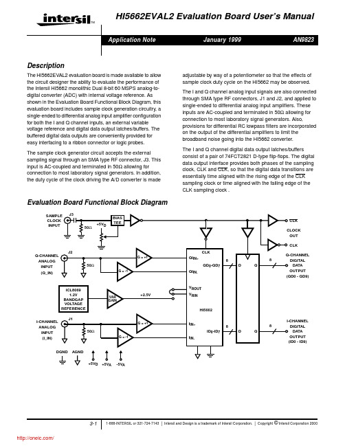
Evaluation Board Layout and Power Supplies
The HI5662 evaluation board is a four layer board with a layout optimized for the best performance of the ADC. Included in the application note are electrical schematics of the evaluation board, a component parts list, a component placement layout drawing and reproductions of the various board layers used in the board stack-up. The user should feel free to copy the layout in their application. Refer to the component layout and the evaluation board electrical schematic for the following discussions.
HI5662EVAL2 Evaluation Board User’s Manual
TM
Application Note
January 1999
AN9823
Description
The HI5662EVAL2 evaluation board is made available to allow the circuit designer the ability to evaluate the performance of the Intersil HI5662 monolithic Dual 8-bit 60 MSPS analog-todigital converter (ADC) with internal voltage reference. As shown in the Evaluation Board Functional Block Diagram, this evaluation board includes sample clock generation circuitry, a single-ended to differential analog input amplifier configuration for both the I and Q channel inputs, an external variable voltage reference and digital data output latches/buffers. The buffered digital data outputs are conveniently provided for easy interfacing to a ribbon connector or logic probes.
Air780 系列 DTU 固件功能用户手册说明书

Air780系列DTU固件功能用户手册V1.0版权声明版权所有:深圳市银尔达电子有限公司。
深圳市银尔达电子有限公司保留所有权利。
说明本应用指南对应产品为适合银尔达全系Air780模块。
本应用指南的使用对象是嵌入式工程师,开发工程师及测试工程师。
深圳市银尔达电子有限公司专注于物联网解决方案,并且为客户提供全方位的技术支持,任何垂询,请直接联系您的客户经理。
公司网站:联系电话:*************联系地址:深圳市龙华区大浪街道中安科技中心A座2003-2005修改记录目录一、产品介绍 (5)1.1、适合Air780系列 (5)1.2、配套使用的文档 (5)二、固件功能描述 (6)三、参数配置基本流程 (8)3.1、参数更新逻辑 (8)3.2、串口和web参数配置的优缺点 (8)3.3、DTU参数配置流程 (9)四、设备恢复出厂设置状态 (10)五、固件性能说明 (11)5.1、串口波特率与数据发送长短的关系 (11)5.2、网络通讯包的长度限制 (11)5.3、UDP限制说明 (11)5.4、MQTT遗嘱说明 (11)5.5、缓存设计说明 (11)5.6、RS485EN翻转速度说明 (12)5.7、TCP心跳包 (12)六、硬件指示灯状态描述 (13)6.1、设备网络状态LED描述 (13)6.2、设备信号强度LED描述 (13)七、网络维护逻辑 (13)八、DTU涉及到的数据描述 (14)九、DTU配置使用 (15)9.1、Web服务器配置 (15)9.2、串口命令配置 (15)十一、免责声明 (16)一、产品介绍本文主要讲解DTU的一些使用注意事项,请务必仔细阅读,对您有效的运用本公司产品会有很大的帮助。
1.1、适合Air780系列固件版本为:YED_DTU2_1.0.1格式的780系列产品。
1.2、配套使用的文档》如果使用Web配置,请参考《银尔达-Air780系列DTU固件Web配置用户手册》》如果使用MCU串口命令去配置参考《银尔达-Air780系列DTU固件串口配置命令手册》并且参考《银尔达-Air780系列DTU固件串口配置命令工程》里面是用串口工具提前写好的可以发送给DTU 的命令》对应产品的硬件规格书二、固件功能描述3.1、参数更新逻辑DTU固件可以使用本地串口配置,也可以使用银尔达web服务器配置参数,两种方法有且只有一个生效。
AD9952 Evaluation Board Datasheet说明书

功能框图图1.DC/PHASE CORRECTION DC/PHASE CORRECTIONC SS C L KS D I OSERIAL PORT INTERFACE15141323892325262838VPOS_3P3DECL1TO DECL4211119303136273340101VPOS_5VLDO VCOLDO 2.5VRFIN0RFIN12922POLYPHASE FILTERLOIN–REFINLOIN+I+I–Q–Q+QUAD DIVIDERPLL343935547611990-001Rev. ADocument FeedbackInformation furnished by Analog Devices is believed to be accurate and reliable. However , no responsibility is assumed by Analog Devices for its use, nor for any infringements of patents or other rights of third parties that may result from its use. Speci cations subject to change without notice. No license is granted by implication or otherwise under any patent or patent rights of Analog Devices. T rademarks and registered trademarks are the property of their respective owners.One Technology Way, P.O. Box 9106, Norwood, MA 02062-9106, U.S.A. Tel: 781.329.4700 ©2013–2014 Analog Devices, Inc. All rights reserved. Technical Support 695 MHz 至2700 MHz 正交解调器,集成小数N 分频PLL 和VCOADRF6820产品特性集成小数N 分频PLL 的I/Q 解调器RF 输入频率范围:695 MHz 至2700 MHz 内部LO 频率范围:356.25 MHz 至2850 MHz 输入P1dB :14.5 dBm (1900 MHz RF) 输入IP3:35 dBm (1900 MHz RF) 可编程HD3/IP3调整单刀双掷(SPDT) RF 输入开关RF 数字步进衰减范围:0 dB 至15 dB集成式RF 可调谐巴伦,支持单端50 Ω输入 多核集成式VCO解调1 dB 带宽:600 MHz 4个可选基带增益和带宽模式数字可编程LO 相位失调和直流零点可通过三线式串行端口接口(SPI)进行编程 40引脚、6 mm x 6 mm LFCSP 封装应用蜂窝W-CDMA/GSM/LTE 数字预失真(DPD)接收器 微波点对点无线电概述ADRF6820是一款高度集成的解调器和频率合成器,非常适合用于下一代通信系统中。
- 1、下载文档前请自行甄别文档内容的完整性,平台不提供额外的编辑、内容补充、找答案等附加服务。
- 2、"仅部分预览"的文档,不可在线预览部分如存在完整性等问题,可反馈申请退款(可完整预览的文档不适用该条件!)。
- 3、如文档侵犯您的权益,请联系客服反馈,我们会尽快为您处理(人工客服工作时间:9:00-18:30)。
12-Bit, SDTV/HDTV 3D Comb Filter,Video Decoder, and Graphics Digitizer Data Sheet ADV7802Rev. DInformation furnished by Analog Devices is believed to be accurate and reliable. However, noresponsibility is assumed by Analog Devices for its use, nor for any infringements of patents or other rights of third parties that may result from its use. Specifications subject to change without notice. No license is granted by implication or otherwise under any patent or patent rights of Analog Devices. T rademarks and registered trademarks are the property of their respective owners. One Technology Way, P.O. Box 9106, N orwood, MA 02062-9106, U.S.A. Tel: 781.329.4700 Fax: 781.461.3113 ©2011Analog Devices, Inc. All rights reserved.FEATURES4 noise shaped video (NSV) 12-bit ADCsTrue 12-bit high dynamic range processing12-channel analog input mux36-bit digital YCrCb/RGB output12-bit deep color processingAnalog monitor outputNTSC/PAL/SECAM color standards supportNTSC/PAL 3D comb filter3D digital noise reduction (DNR)Advanced time-base correction (TBC) with frame synchronizationInterlaced-to-progressive conversion for 525i and 625i Advanced VBI data slicer, including teletext, CC, and V-chip IF compensation filterSCART fast blank support including slow switch detect Programmable internal antialias filtersWeak, poor time-base, and nonstandard signal support Vertical peaking, horizontal peaking, CTI, LTI Simultaneous interlaced and progressive parallel output for 525i/525p and 625i/625p525p/625p component progressive scan support720p/1080i/1080p component HDTV supportDigitizes RGB graphics with maximum pixel clock rate of 135 MHz (ADV7802BSTZ-150 model only)24-bit digital input port supports data from DVI/HDMI Rx IC Any-to-any, advanced 3 × 3 color space conversion matrix Flexible output pixel interface supporting 8-/10-/12-/16-/ 20-/24-/30-/36-bit SDR/DDR 4:2:2/4:4:4 data formats Programmable interrupt request output pin APPLICATIONSAV receiversLCD HDTVsPDP HDTVsCRT HDTVsHDTV STBs with PVRDVD recorders with progressive scan input support ProjectorsFigure 1. ADV7802 Block DiagramGENERAL DESCRIPTIONThe ADV78021 is a high quality, single-chip, multiformat 3D comb filter, video decoder, and graphics digitizer. This multiformat 3D comb filter decoder supports the conversion of PAL, NTSC, and SECAM standards in the form of a composite or an S-video into a digital ITU-R BT.656 format. The ADV7802 also supports the decoding of a component RGB/YPrPb video signal into a digital YCrCb or RGB pixel output stream.The support for component video includes standards such as 525i, 625i, 525p, 625p, 720p, 1080i, 1080p, and many other HD and SMPTE standards. Graphics digitization is supported by theADV7802; it is capable of digitizing RGB graphics signals from VGA to SXGA rates and converting them into a digital RGB or YCrCb pixel output stream. SCART and overlay functionality are enabled by the ability of the ADV7802 to simultaneously process CVBS and standard definition RGB signals.The ADV7802 contains two main processing sections. The first section is the standard definition processor (SDP), which processes all PAL, NTSC, SECAM, and component (up to525p/625p) signal types. The second section is the component processor (CP), which processes YPrPb and RGB component formats, including RGB graphics.1Protected by U.S. Patent Number 4,907,093 and other intellectualproperty rights.ADV7802Data SheetRev. D | Page 2 of 36TABLE OF CONTENTSFeatures .............................................................................................. 1 Applications ....................................................................................... 1 General Description ......................................................................... 1 Revision History ............................................................................... 2 Functional Block Diagram .............................................................. 3 Specifications ..................................................................................... 4 Electrical Characteristics ............................................................. 4 Video Specifications ..................................................................... 6 Timing Characteristics ................................................................ 7 Timing Diagrams .......................................................................... 8 Analog Specifications ................................................................... 9 Absolute Maximum Ratings .......................................................... 10 Package Thermal Performance ................................................. 10 Thermal Resistance .................................................................... 10 ESD Caution ................................................................................ 10 Pin Configuration and Function Descriptions ........................... 11 Theory of Operation ...................................................................... 14 Key Features ................................................................................ 14 Analog Front End ....................................................................... 14 Standard Definition Processor ................................................. 14 VBI Data Processor .................................................................... 15 Component Processor ............................................................... 15 Additional Features .................................................................... 16 Single Data Rate (SDR) .............................................................. 16 Double Data Rate (DDR) .......................................................... 16 Recommended External Loop Filter Components .................... 17 Typical Connection Diagrams ...................................................... 18 Pixel Input/Output Formatting .................................................... 21 Pixel Data Output Modes Highlights ...................................... 21 Digital Video Input Port Highlights ........................................ 21 Outline Dimensions ....................................................................... 34 Ordering Guide .. (34)REVISION HISTORY8/11—Revision D: Initial VersionData SheetADV7802Rev. D | Page 3 of 36FUNCTIONAL BLOCK DIAGRAMS -S (C B V S +G R A P H I C C V B F H P 30 T V H V L D A T A O P 53S _O U TU TD E _O U TS Y N C _O U T06654-002Figure 2.ADV7802 Data Sheet SPECIFICATIONSELECTRICAL CHARACTERISTICSAVDD = 3.15 V to 3.45 V, DVDD = 1.75 V to 1.85 V, DVDDIO = 3.0 V to 3.6 V, DVDDIO_SDRAM = 2.35 V to 2.65 V (DDR), DVDDIO_SDRAM = 3.2 V to 3.4 V (SDR), PVDD = 1.71 V to 1.89 V, nominal input range 1.6 V. T A = 0°C to 85°C, unlessotherwise noted.Table 1.Parameter1Symbol Test Conditions Min Typ Max Unit STATIC PERFORMANCE2, 3Resolution (Each ADC) N 12 Bits Integral Nonlinearity4INL BSL at 27 MHz (at a 12-bit level) −1.0/+1.5 LSBBSL at 54 MHz (at a 12-bit level) −1.5/+2.0 LSBBSL at 74 MHz (at an 11-bit level) −1.4/+1.2 LSBBSL at 110 MHz (at a 10-bit level) −0.8/+2.0 LSBBSL at 150 MHz (at an 8-bit level) −2.0/+2.0 LSB Differential Nonlinearity4DNL At 27 MHz (at a 12-bit level) −0.6/+0.7 LSBAt 54 MHz (at a 12-bit level) −0.6/+0.8 LSBAt 74 MHz (at an 11-bit level) −0.9/+0.75 LSBAt 110 MHz (at a 10-bit level) −0.5/+1.0 LSBAt 150 MHz (at an 8-bit level) −0.7/+1.5 LSB POWER REQUIREMENTS5Digital Core Power Supply DVDD 1.75 1.8 1.85 V Digital I/O Power Supply DVDDIO 3.0 3.3 3.6 V PLL Power Supply PVDD 1.71 1.8 1.89 V Analog Power Supply AVDD 3.15 3.3 3.45 V Memory Interface Power Supply DVDDIO_SDRAM DDR 2.35 2.5 2.65 VSDR 3.2 3.3 3.4 V Digital Core Supply Current I DVDD CVBS input sampling at 54 MHz 236 mAGraphics RGB sampling at 78 MHz 103 mASCART RGB FB sampling at 54 MHz 236 mA525p input sampling at 54 MHz 319 mAGraphics RGB sampling at 135 MHz 180 mA1080p sampling at 148.5 MHz 214 mA Digital I/O Supply Current I DVDDIO CVBS input sampling at 54 MHz 6 mAGraphics RGB sampling at 78 MHz 15 mAGraphics RGB sampling at 135 MHz 27 mA1080p sampling at 148.5 MHz 48 mA PLL Supply Current I PVDD CVBS input sampling at 54 MHz 13 mAGraphics RGB sampling at 78 MHz 10 mAGraphics RGB sampling at 135 MHz 10 mA1080p sampling at 148.5 MHz 11 mA Analog Supply Current I AVDD CVBS input sampling at 54 MHz 99 mASCART RGB FB sampling at 54 MHz 269 mAGraphics RGB sampling at 78 MHz 263 mAGraphics RGB sampling at 135 MHz 286 mA1080p sampling at 148.5 MHz 288 mA Memory Interface Supply Current I VDDRAM CVBS input sampling at 54 MHz 17 mA Power-Down Current I PWRDN8 mA Power-Up Time t PWRUP20 ms DIGITAL INPUTSInput High Voltage V IH 2 V Input Low Voltage V IL0.8 V Input Current I IN±10 µA Input Capacitance C IN15 pFRev. D | Page 4 of 36Data SheetADV7802Rev. D | Page 5 of 36Parameter 1Symbol Test Conditions Min Typ Max Unit DIGITAL OUTPUTSOutput High Voltage 6 V OH I SOURCE = 0.4 mA 2.4 V Output Low Voltage 6V OL I SINK = 3.2 mA 0.4 V High Impedance Leakage Current I LEAK 10 μA Output CapacitanceC OUT20pF1Temperature range T MIN to T MAX .2All ADC linearity tests performed with part configured for component video input. 3All ADC linearity tests performed at input range of full scale − 12.5% and at zero scale + 12.5%. 4Maximum INL and DNL specifications obtained with part configured for component video input. 5Guaranteed by characterization. 6V OH and V OL levels obtained using default drive strength.ADV7802Data SheetRev. D | Page 6 of 36VIDEO SPECIFICATIONSAVDD = 3.15 V to 3.45 V , DVDD = 1.75 V to 1.85 V , DVDDIO = 3.0 V to 3.6 V , DVDDIO_SDRAM = 2.4 V to 2.6 V (DDR), DVDDIO_SDRAM = 3.2 V to 3.4 V (SDR), PVDD = 1.71 V to 1.89 V , T A = 0°C to 85°C, unless otherwise noted. Table 2.Parameter 1Symbol Test Conditions Min Typ Max Unit NONLINEAR SPECIFICATIONSDifferential Phase DP CVBS input (modulated five-step) 0.45 Degrees Differential Gain DG CVBS input (modulated five-step) 0.45 % Luma Nonlinearity LNL CVBS input (modulated five-step) 0.7 % NOISE SPECIFICATIONSSNR Unweighted Luma ramp 63 dBLuma flat field 64 dB Analog Front-End Crosstalk 60 dB LOCK TIME SPECIFICATIONS (SDP) Horizontal Lock Range ±5 % Vertical Lock Range40 70 Hz Subcarrier Lock Range, f SC ±0.8 kHz Color Lock-In Time 60 Lines Sync Depth Range 2 20 200 % Color Burst Range 1 200 % Vertical Lock Time 300 ms Horizontal Lock Time100 Lines CHROMA SPECIFICATIONS (SDP) Chroma Amplitude Error 0.4 %Chroma Phase Error0.3 Degrees Chroma Luma Intermodulation0.2 %1 Guaranteed by characterization.2Nominal sync depth is 300 mV at 100% sync depth range.Data SheetADV7802Rev. D | Page 7 of 36TIMING CHARACTERISTICSAVDD = 3.15 V to 3.45 V , DVDD = 1.75 V to 1.85 V , DVDDIO = 3.0 V to 3.6 V , DVDDIO_SDRAM = 2.4 V to 2.6 V (DDR), DVDDIO_SDRAM = 3.2 V to 3.4 V (SDR), PVDD = 1.71 V to 1.89 V , T A = 0°C to 85°C, unless otherwise noted. Table 3.Parameter 1Symbol Test Conditions Min Typ Max Unit SYSTEM CLOCK AND CRYSTALCrystal Nominal Frequency 28.63636 MHz Crystal Frequency Stability±50 ppm Horizontal Sync Input Frequency 14.8 90 kHz LLC Frequency Range 12.825 150 MHz I 2C PORTSCLK Frequency400 kHz SCLK Minimum Pulse Width High t 1 0.6 µs SCLK Minimum Pulse Width Low t 2 1.3 µs Hold Time (Start Condition) t 3 0.6 µs Setup Time (Start Condition) t 4 0.6 µs SDA Setup Timet 5 100 ns SCLK and SDA Rise Time t 6 300 ns SCLK and SDA Fall Time t 7 300 ns Setup Time (Stop Condition) t 8 0.6 µs FAST I 2C PORT 2 SCLK Frequency3.4 MHz SCLK Minimum Pulse Width High t 1 60 ns SCLK Minimum Pulse Width Low t 2 160 ns Hold Time (Start Condition) t 3 160 ns Setup Time (Start Condition) t 4 160 ns SDA Setup Timet 5 10 ns SCLK and SDA Rise Time t 6 10 80 ns SCLK and SDA Fall Time t 7 10 80 ns Setup Time (Stop Condition) t 8 160 ns RESET FEATUREReset Pulse Width 5 ms CLOCK OUTPUTSLLC Mark Space Ratiot 9, t 10 45:55 55:45 % duty cycle PIXEL PORT DATA AND CONTROL OUTPUTS 3Data Output Transition Time, SDR t 11 Negative clock edge to start of valid data4.5 ns Data Output Transition Time, SDR t 12 End of valid data to negative clock edge0 ns Data Output Transition Time, SDR (CP Core) t 13 Negative clock edge to start of valid data2.5 ns Data Output Transition Time, SDR (CP Core) t 14 End of valid data to negative clock edge 0.2 ns DATA AND CONTROL INPUTS 4Input Setup Time (Digital Input Port) t 17 HS_IN1, VS_IN1, HS_IN2, VS_IN2 9.5 nsDE_IN, data inputs2 ns Input Hold Time (Digital Input Port) t 18 HS_IN1, VS_IN1, HS_IN2, VS_IN2 −4 nsDE_IN, data inputs0.8ns1 Guaranteed by characterization. 2With a bus line load less than 100 pF. 3Timing figures obtained using default drive strength value. 4TTL input values are 0 V to 3 V, with rise/fall times ≥ 3 ns, measured between the 10% and 90% points.ADV7802Data SheetRev. D | Page 8 of 36TIMING DIAGRAMS06654-004Figure 3. I 2C Timing06654-005Figure 4. Pixel Port and Control SDR Output Timing (SD Core)06654-011Figure 5. Pixel Port and Control SDR Output Timing (CP Core)CONTROL INPUTSP30 TO P39,P40 TO P43,P44 TO P53HS_IN1,VS_IN1,HS_IN2,VS_IN2,DE_IN06654-007Figure 6. Digital Input Port and Control Input TimingData SheetADV7802Rev. D | Page 9 of 36ANALOG SPECIFICATIONSAVDD = 3.15 V to 3.45 V , DVDD = 1.75 V to 1.85 V , DVDDIO = 3.0 V to 3.6 V , DVDDIO_SDRAM = 2.4 V to 2.6 V (DDR),DVDDIO_SDRAM = 3.2 V to 3.4 V (SDR), PVDD = 1.71 V to 1.89 V , T A = 0°C to 85°C, unless otherwise noted. Recommended analog input video signal range is 0.5 V to 1.6 V , typically 1 V p-p. Recommended external clamp capacitor value is 0.1 μF. Table 4.Parameter 1, 2 Test Conditions Min Typ Max Unit CLAMP CIRCUITRYInput Impedance 3Clamps switched off 10 MΩ Input Impedance of Pin 90 (FB) 20 kΩ CML2.0V ADC Full-Scale Level CML + 0.8 V ADC Zero-Scale Level CML − 0.8 V ADC Dynamic Range1.6V Clamp Level (When Locked) CVBS inputCML − 0.292 V SCART RGB input (R, G, B signals) CML − 0.3 V S-Video input (Y signal) CML − 0.292 V S-Video input (C signal) CML − 0 V Component input (Y signal)CML − 0.3 V Component input (Pr, Pb signals) CML − 0 VPC RGB input (R, G, B signals) CML − 0.3 V Large Clamp Source Current SDP only 0.75 mA Large Clamp Sink Current SDP only 0.9 mA Fine Clamp Source Current SDP only 17 µA Fine Clamp Sink CurrentSDP only 17 µA1 The minimum/maximum specifications are guaranteed over 0°C to 85°C. 2Guaranteed by characterization. 3Except Pin 90 (FB).ADV7802Data SheetRev. D | Page 10 of 36ABSOLUTE MAXIMUM RATINGSTable 5.Parameter Rating AVDD to AGND 4.0 V DVDD to DGND 2.2 V PVDD to AGND 2.2 V DVDDIO to DGND 4.0 V DVDDIO_SDRAM to DGND_SDRAM (DDR) 2.7 V DVDDIO_SDRAM to DGND_SDRAM (SDR) 4.0 V DVDDIO to AVDD −0.3 V to +0.3 V DVDDIO to DVDD −0.3 V to +2 V DVDDIO_SDRAM to DVDD (DDR) −0.3 V to +2.5 V DVDDIO_SDRAM to DVDD (SDR) −0.3 V to +3.3 V AVDD to PVDD −0.3 V to +2 V AVDD to DVDD −0.3 V to +2 V DVDDIO to DVDDIO_SDRAM (DDR) −0.3 V to +2 V DVDDIO to DVDDIO_SDRAM (SDR) −0.3 V to +3.3 V AVDD to DVDDIO_SDRAM (DDR) −0.3 V to +2.5 V AVDD to DVDDIO_SDRAM (SDR) −0.3 V to +1.8 V Digital Inputs Voltage to DGND DGND − 0.3 V to DVDDIO + 0.3 V DVDDIO_SDRAM Inputs to DGND_SDRAM DGND_SDRAM − 0.3 V to DVDDIO_SDRAM + 0.3 V Analog Inputs to AGND AGND − 0.3 V to AVDD + 0.3 V SCLK/SDA Data Pins to DVDDIO DVDDIO − 0.3 V to DVDDIO + 3.6 VMaximum Junction Temperature(T J MAX )125°C Storage Temperature Range −65°C to +150°C Infrared Reflow Soldering (20 sec) 260°CStresses above those listed under Absolute Maximum Ratings may cause permanent damage to the device. This is a stress rating only; functional operation of the device at these or any other conditions above those indicated in the operationalsection of this specification is not implied. Exposure to absolute maximum rating conditions for extended periods may affect device reliability.PACKAGE THERMAL PERFORMANCETo reduce power consumption when using the part, the user is advised to turn off any unused ADCs.The junction temperature must always stay below the maximum junction temperature (T J MAX ) of 125°C. The following equation shows how to calculate the junction temperature:T J = T A MAX + (θJA × W MAX )where:T A MAX = 85°C. θJA = 21.0330°C/W.W MAX = ((A VDD × I A VDD ) + (DVDD × I DVDD ) + (DVDDIO × I DVDDIO ) + (PVDD × I PVDD ) + (DVDDIO_SDRAM × DVDDIO_SDRAM)).THERMAL RESISTANCEθJA is specified for the worst-case conditions, that is, a device soldered in a circuit board for surface-mount packages. Table 6. Thermal ResistancePackage Type θJA 1 θJC 2 Unit 176-Lead LQFP21 7 °C/W1 4-layer PCB with solid ground plane.24-layer PCB with solid ground plane (still air).ESD CAUTION分销商库存信息: ANALOG-DEVICES EVAL-ADV7802EB1Z。