VI-2TYEY中文资料
HD74LS02P中文资料

HD74LS02Quadruple 2-Input Positive NOR GatesREJ03D0389–0200Rev.2.00Feb.18.2005 Features• Ordering InformationPart Name Package Type Package Code(Previous Code)PackageAbbreviationTaping Abbreviation(Quantity)HD74LS02P DILP-14pin PRDP0014AB-B(DP-14AV)P —HD74LS02FPEL SOP-14 pin (JEITA) PRSP0014DF-B(FP-14DAV)FP EL (2,000 pcs/reel)HD74LS02RPEL SOP-14 pin (JEDEC) PRSP0014DE-A(FP-14DNV)RP EL (2,500 pcs/reel)Note: Please consult the sales office for the above package availability. Pin ArrangementCircuit Schematic (1/4)Absolute Maximum RatingsUnitRatingsItem SymbolSupply voltage V CC Note 7 VInput voltage V IN 7 V Power dissipation P T 400 mW Storage temperature Tstg –65 to +150 °CNote: Voltage value, unless otherwise noted, are with respect to network ground terminal.Recommended Operating ConditionsUnitMaxItem SymbolMinTypSupply voltage V CC 4.75 5.00 5.25 VI OH — — –400 µAOutput currentI OL — — 8 mA°C7525–20Operating temperature ToprElectrical Characteristics(Ta = –20 to +75 °C)ItemSymbol min. typ.* max. Unit Condition V IH 2.0 — — V Input voltageV IL — — 0.8 V V OH 2.7 — — V V CC = 4.75 V, V IL = 0.8 V, I OH = –400 µA— — 0.5 I OL = 8 mAOutput voltageV OL— — 0.4 V I OL = 4 mAV CC = 4.75 V, V IH = 2 V I IH — — 20 µA V CC = 5.25 V, V I = 2.7 V I IL — — –0.4 mA V CC = 5.25 V, V I = 0.4 VInput current I I — — 0.1 mA V CC = 5.25 V, V I = 7 V Short-circuit outputcurrent I OS –20— –100 mA V CC = 5.25 V I CCH — 1.6 3.2 mA V CC = 5.25 VSupply currentI CCL — 2.8 5.4 mA V CC = 5.25 VInput clamp voltage V IK — — –1.5 V V CC = 4.75 V, I IN = –18 mA Note: * V CC = 5 V, Ta = 25°CSwitching Characteristics(V CC = 5 V, Ta = 25°C)Item Symbol min. typ. max. Unit Conditiont PLH — 10 15 nsPropagation delay time t PHL — 10 15 ns C L = 15 pF, R L = 2 k ΩNote: Refer to Test Circuit and Waveform of the Common Item "TTL Common Matter (Document No.: REJ27D0005-0100)".Package Dimensions RENESAS SALES OFFICESRefer to "/en/network" for the latest and detailed information.Renesas Technology America, Inc.450 Holger Way, San Jose, CA 95134-1368, U.S.ATel: <1> (408) 382-7500, Fax: <1> (408) 382-7501Renesas Technology Europe LimitedDukes Meadow, Millboard Road, Bourne End, Buckinghamshire, SL8 5FH, U.K.Tel: <44> (1628) 585-100, Fax: <44> (1628) 585-900Renesas Technology Hong Kong Ltd.7th Floor, North Tower, World Finance Centre, Harbour City, 1 Canton Road, Tsimshatsui, Kowloon, Hong KongTel: <852> 2265-6688, Fax: <852> 2730-6071Renesas Technology Taiwan Co., Ltd.10th Floor, No.99, Fushing North Road, Taipei, TaiwanTel: <886> (2) 2715-2888, Fax: <886> (2) 2713-2999Renesas Technology (Shanghai) Co., Ltd.Unit2607 Ruijing Building, No.205 Maoming Road (S), Shanghai 200020, ChinaTel: <86> (21) 6472-1001, Fax: <86> (21) 6415-2952Renesas Technology Singapore Pte. Ltd.1 Harbour Front Avenue, #06-10, Keppel Bay Tower, Singapore 098632Tel: <65> 6213-0200, Fax: <65> 6278-8001。
74HC00中文资料_数据手册_参数
IO = −20 µA
2.0
IO = −20 µA
4.5
IO = −20 µA
6.0
IO = −4.0 mA
4.5
IO = −5.2 mA
6.0
VOL
LOW-level output voltage VI = VIH or VIL
IO = 20 µA
2.0
IO = 20 µA
4.5
IO = 20 µA
RECOMMENDED OPERATING CONDITIONS
SYMBOL
PARAMETER
VCC VI VO Tamb
supply voltage input voltage output voltage operating ambient temperature
tr, tf
input rise and fall times
74HC00; 74HCT00
handbook, halfpage
1B 2
1A VCC 1 14
13 4B
1Y 3
12 4A
2A 4 2B 5
GND(1)
11 4Y 10 3B
2Y 6 78
Top view GND 3Y
9 3A
MNA950
handbook, halfpage A B
Y
MNA211
(1) The die substrate is attached to this pad using conductive die attach material. It can not be used as a supply pin or input.
6.0
IO = 4.0 mA
HD74LS04P中文资料
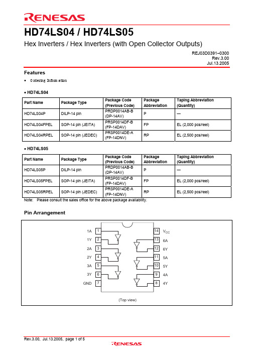
HD74LS04 / HD74LS05Hex Inverters / Hex Inverters (with Open Collector Outputs)REJ03D0391–0300Rev.3.00Jul.13.2005 Features• Ordering Information• HD74LS04Part Name Package Type Package Code(Previous Code)PackageAbbreviationTaping Abbreviation(Quantity)HD74LS04P DILP-14pin PRDP0014AB-B(DP-14AV)P —HD74LS04FPEL SOP-14 pin (JEITA) PRSP0014DF-B(FP-14DAV)FP EL (2,000 pcs/reel)HD74LS04RPEL SOP-14 pin (JEDEC) PRSP0014DE-A(FP-14DNV)RP EL (2,500 pcs/reel)• HD74LS05Part Name Package Type Package Code(Previous Code)PackageAbbreviationTaping Abbreviation(Quantity)HD74LS05P DILP-14pin PRDP0014AB-B(DP-14AV)P —HD74LS05FPEL SOP-14 pin (JEITA) PRSP0014DF-B(FP-14DAV)FP EL (2,000 pcs/reel)HD74LS05RPEL SOP-14 pin (JEDEC) PRSP0014DE-A(FP-14DNV)RP EL (2,500 pcs/reel)Note: Please consult the sales office for the above package availability. Pin ArrangementCircuit Schematic (1/6)Absolute Maximum RatingsUnitRatingsItem SymbolSupply voltage V CC Note 7 VInput voltage V IN 7 V Power dissipation P T 400 mW Storage temperature Tstg –65 to +150 °CNote: Voltage value, unless otherwise noted, are with respect to network ground terminal.Recommended Operating Conditions• HD74LS04MaxUnitMinTypItem SymbolSupply voltage V CC 4.75 5.00 5.25 VI OH — — –400 µAOutput currentI OL — — 8 mA°C2575Operating temperature Topr–20• HD74LS05MaxUnitTypMinItem SymbolSupply voltage V CC 4.75 5.00 5.25 VOutput voltage V OH — — 5.5 VOutput current I OL — — 8 mA°C7525–20Operating temperature ToprElectrical Characteristics• HD74LS04(Ta = –20 to +75 °C)ItemSymbol min. typ.* max. Unit Condition V IH 2.0 — — V Input voltageV IL — — 0.8 V V OH 2.7 — — V V CC = 4.75 V, V IL = 0.8 V, I OH = –400 µA— — 0.5 I OL = 8 mAOutput voltageV OL— — 0.4 V I OL = 4 mAV CC = 4.75 V, V IH = 2 V I IH — — 20 µA V CC = 5.25 V, V I = 2.7 V I IL — — –0.4 mA V CC = 5.25 V, V I = 0.4 VInput current I I — — 0.1 mA V CC = 5.25 V, V I = 7 V Short-circuit outputcurrent I OS –20— –100 mA V CC = 5.25 V I CCH — 1.2 2.4 mA V CC = 5.25 VSupply currentI CCL — 3.6 6.6 mA V CC = 5.25 VInput clamp voltage V IK — — –1.5 V V CC = 4.75 V, I IN = –18 mA Note: * V CC = 5 V, Ta = 25°C• HD74LS05(Ta = –20 to +75 °C)ItemSymbol min. typ.* max. Unit Condition V IH 2.0 — — VInput voltageV IL — — 0.8 V— — 0.5 I OL = 8 mAOutput voltage V OL — — 0.4 V I OL = 4 mAV CC = 4.75 V, V IH = 2 VOutput current I OH — — 100 µA V CC = 4.75 V, V IL = 0.8 V, V OA = 5.5 VI IH — — 20 µA V CC = 5.25 V, V I = 2.7 VI IL — — –0.4 mA V CC = 5.25 V, V I = 0.4 VInput current I I —— 0.1 mA V CC = 5.25 V, V I = 7 V I CCH — 1.2 2.4 mA V CC = 5.25 VSupply currentI CCL —3.6 6.6 mA V CC = 5.25 V Input clamp voltage V IK — — –1.5 V V CC =4.75 V, I IN = –18 mA Note: * V CC = 5 V, Ta = 25°CSwitching Characteristics• HD74LS04(V CC = 5 V, Ta = 25°C)Item Symbol min. typ. max. Unit Conditiont PLH — 9 15 nsPropagation delay timet PHL — 10 15 ns C L = 15 pF, R L = 2 k Ω• HD74LS05(V CC = 5 V, Ta = 25°C)Item Symbol min. typ. max. Unit Conditiont PLH — 17 32 nsPropagation delay time t PHL — 15 28 nsC L = 15 pF, R L = 2 k ΩNote: Refer to Test Circuit and Waveform of the Common Item "TTL Common Matter (Document No.: REJ27D0005-0100)".Package Dimensions RENESAS SALES OFFICESRefer to "/en/network" for the latest and detailed information.Renesas Technology America, Inc.450 Holger Way, San Jose, CA 95134-1368, U.S.ATel: <1> (408) 382-7500, Fax: <1> (408) 382-7501Renesas Technology Europe LimitedDukes Meadow, Millboard Road, Bourne End, Buckinghamshire, SL8 5FH, U.K.Tel: <44> (1628) 585-100, Fax: <44> (1628) 585-900Renesas Technology Hong Kong Ltd.7th Floor, North Tower, World Finance Centre, Harbour City, 1 Canton Road, Tsimshatsui, Kowloon, Hong KongTel: <852> 2265-6688, Fax: <852> 2730-6071Renesas Technology Taiwan Co., Ltd.10th Floor, No.99, Fushing North Road, Taipei, TaiwanTel: <886> (2) 2715-2888, Fax: <886> (2) 2713-2999Renesas Technology (Shanghai) Co., Ltd.Unit2607 Ruijing Building, No.205 Maoming Road (S), Shanghai 200020, ChinaTel: <86> (21) 6472-1001, Fax: <86> (21) 6415-2952Renesas Technology Singapore Pte. Ltd.1 Harbour Front Avenue, #06-10, Keppel Bay Tower, Singapore 098632Tel: <65> 6213-0200, Fax: <65> 6278-8001Renesas Technology Korea Co., Ltd.Kukje Center Bldg. 18th Fl., 191, 2-ka, Hangang-ro, Yongsan-ku, Seoul 140-702, KoreaTel: <82> 2-796-3115, Fax: <82> 2-796-2145Renesas Technology Malaysia Sdn. Bhd.Unit 906, Block B, Menara Amcorp, Amcorp Trade Centre, No.18, Jalan Persiaran Barat, 46050 Petaling Jaya, Selangor Darul Ehsan, MalaysiaTel: <603> 7955-9390, Fax: <603> 7955-9510。
HD74LV2GT34AUSE中文资料

Recommended Operating Conditions
Item Supply voltage range Input voltage range Output voltage range Output current Symbol VCC VI VO IOL IOH Input transition rise or fall rate ∆t / ∆v Operating free-air temperature Ta Min 3.0 0 0 — — — — 0 0 –40 Note: Unused or floating inputs must be held high or low. Max 5.5 5.5 VCC 6 12 –6 –12 100 20 85 °C ns / V Unit V V V mA VCC = 3.0 to 3.6 V VCC = 4.5 to 5.5 V VCC = 3.0 to 3.6 V VCC = 4.5 to 5.5 V VCC = 3.0 to 3.6 V VCC = 4.5 to 5.5 V Conditions
Ta = 25°C Item Propagation delay time Symbol tPLH tPHL Min — — Typ 6.5 11.0 Max 12.0 15.0
Ta = –40 to 85°C
Test Unit Conditions ns CL = 15 pF CL = 50 pF
The HD74LV2GT34A has triple noninverters in an 8 pin package. The input protection circuitry on this device allows over voltage tolerance on the input, allowing the device to be used as a logic–level translator from 3.0 V CMOS Logic to 5.0 V CMOS Logic or from 1.8 V CMOS logic to 3.0 V CMOS Logic while operating at the high-voltage power supply. Low voltage and high-speed operation is suitable for the battery powered products (e.g., notebook computers), and the low power consumption extends the battery life.
LV244A中文资料

PACKAGING INFORMATIONOrderable Device Status(1)PackageType PackageDrawingPins PackageQtyEco Plan(2)Lead/Ball Finish MSL Peak Temp(3)SN74LV244ADBLE OBSOLETE SSOP DB20TBD Call TI Call TISN74LV244ADBR ACTIVE SSOP DB202000Green(RoHS&no Sb/Br)CU NIPDAU Level-1-260C-UNLIMSN74LV244ADBRE4ACTIVE SSOP DB202000Green(RoHS&no Sb/Br)CU NIPDAU Level-1-260C-UNLIMSN74LV244ADGVR ACTIVE TVSOP DGV202000Green(RoHS&no Sb/Br)CU NIPDAU Level-1-260C-UNLIMSN74LV244ADGVRE4ACTIVE TVSOP DGV202000Green(RoHS&no Sb/Br)CU NIPDAU Level-1-260C-UNLIMSN74LV244ADW ACTIVE SOIC DW2025Green(RoHS&no Sb/Br)CU NIPDAU Level-1-260C-UNLIMSN74LV244ADWE4ACTIVE SOIC DW2025Green(RoHS&no Sb/Br)CU NIPDAU Level-1-260C-UNLIMSN74LV244ADWR ACTIVE SOIC DW202000Green(RoHS&no Sb/Br)CU NIPDAU Level-1-260C-UNLIMSN74LV244ANSR ACTIVE SO NS202000Green(RoHS&no Sb/Br)CU NIPDAU Level-1-260C-UNLIMSN74LV244ANSRE4ACTIVE SO NS202000Green(RoHS&no Sb/Br)CU NIPDAU Level-1-260C-UNLIMSN74LV244ANSRG4ACTIVE SO NS202000Green(RoHS&no Sb/Br)CU NIPDAU Level-1-260C-UNLIMSN74LV244APW ACTIVE TSSOP PW2070Green(RoHS&no Sb/Br)CU NIPDAU Level-1-260C-UNLIMSN74LV244APWE4ACTIVE TSSOP PW2070Green(RoHS&no Sb/Br)CU NIPDAU Level-1-260C-UNLIMSN74LV244APWG4ACTIVE TSSOP PW2070Green(RoHS&no Sb/Br)CU NIPDAU Level-1-260C-UNLIM SN74LV244APWLE OBSOLETE TSSOP PW20TBD Call TI Call TISN74LV244APWR ACTIVE TSSOP PW202000Green(RoHS&no Sb/Br)CU NIPDAU Level-1-260C-UNLIMSN74LV244APWRE4ACTIVE TSSOP PW202000Green(RoHS&no Sb/Br)CU NIPDAU Level-1-260C-UNLIMSN74LV244APWRG4ACTIVE TSSOP PW202000Green(RoHS&no Sb/Br)CU NIPDAU Level-1-260C-UNLIMSN74LV244APWT ACTIVE TSSOP PW20250Green(RoHS&no Sb/Br)CU NIPDAU Level-1-260C-UNLIMSN74LV244APWTE4ACTIVE TSSOP PW20250Green(RoHS&no Sb/Br)CU NIPDAU Level-1-260C-UNLIMSN74LV244ARGYR ACTIVE QFN RGY201000Green(RoHS&no Sb/Br)CU NIPDAU Level-2-260C-1YEAR SN74LV244ARGYRG4ACTIVE QFN RGY20TBD Call TI Call TI(1)The marketing status values are defined as follows:ACTIVE:Product device recommended for new designs.LIFEBUY:TI has announced that the device will be discontinued,and a lifetime-buy period is in effect.NRND:Not recommended for new designs.Device is in production to support existing customers,but TI does not recommend using this part in a new design.PREVIEW:Device has been announced but is not in production.Samples may or may not be available.OBSOLETE:TI has discontinued the production of the device.(2)Eco Plan-The planned eco-friendly classification:Pb-Free(RoHS),Pb-Free(RoHS Exempt),or Green(RoHS&no Sb/Br)-please check /productcontent for the latest availability information and additional product content details.TBD:The Pb-Free/Green conversion plan has not been defined.Pb-Free(RoHS):TI's terms"Lead-Free"or"Pb-Free"mean semiconductor products that are compatible with the current RoHS requirements for all6substances,including the requirement that lead not exceed0.1%by weight in homogeneous materials.Where designed to be soldered at high temperatures,TI Pb-Free products are suitable for use in specified lead-free processes.Pb-Free(RoHS Exempt):This component has a RoHS exemption for either1)lead-based flip-chip solder bumps used between the die and package,or2)lead-based die adhesive used between the die and leadframe.The component is otherwise considered Pb-Free(RoHS compatible)as defined above.Green(RoHS&no Sb/Br):TI defines"Green"to mean Pb-Free(RoHS compatible),and free of Bromine(Br)and Antimony(Sb)based flame retardants(Br or Sb do not exceed0.1%by weight in homogeneous material)(3)MSL,Peak Temp.--The Moisture Sensitivity Level rating according to the JEDEC industry standard classifications,and peak solder temperature.Important Information and Disclaimer:The information provided on this page represents TI's knowledge and belief as of the date that it is provided.TI bases its knowledge and belief on information provided by third parties,and makes no representation or warranty as to the accuracy of such information.Efforts are underway to better integrate information from third parties.TI has taken and continues to take reasonable steps to provide representative and accurate information but may not have conducted destructive testing or chemical analysis on incoming materials and chemicals.TI and TI suppliers consider certain information to be proprietary,and thus CAS numbers and other limited information may not be available for release.In no event shall TI's liability arising out of such information exceed the total purchase price of the TI part(s)at issue in this document sold by TI to Customer on an annual basis.元器件交易网IMPORTANT NOTICETexas Instruments Incorporated and its subsidiaries (TI) reserve the right to make corrections, modifications,enhancements, improvements, and other changes to its products and services at any time and todiscontinue any product or service without notice. Customers should obtain the latest relevant informationbefore placing orders and should verify that such information is current and complete. All products are soldsubject to TI’s terms and conditions of sale supplied at the time of order acknowledgment.TI warrants performance of its hardware products to the specifications applicable at the time of sale inaccordance with TI’s standard warranty. Testing and other quality control techniques are used to the extentTI deems necessary to support this warranty. Except where mandated by government requirements, testingof all parameters of each product is not necessarily performed.TI assumes no liability for applications assistance or customer product design. Customers are responsiblefor their products and applications using TI components. To minimize the risks associated with customerproducts and applications, customers should provide adequate design and operating safeguards.TI does not warrant or represent that any license, either express or implied, is granted under any TI patentright, copyright, mask work right, or other TI intellectual property right relating to any combination, machine,or process in which TI products or services are used. Information published by TI regarding third-partyproducts or services does not constitute a license from TI to use such products or services or a warranty orendorsement thereof. Use of such information may require a license from a third party under the patents orother intellectual property of the third party, or a license from TI under the patents or other intellectualproperty of TI.Reproduction of information in TI data books or data sheets is permissible only if reproduction is withoutalteration and is accompanied by all associated warranties, conditions, limitations, and notices.Reproduction of this information with alteration is an unfair and deceptive business practice. TI is notresponsible or liable for such altered documentation.Resale of TI products or services with statements different from or beyond the parameters stated by TI forthat product or service voids all express and any implied warranties for the associated TI product or serviceand is an unfair and deceptive business practice. TI is not responsible or liable for any such statements.Following are URLs where you can obtain information on other Texas Instruments products and applicationsolutions:Products ApplicationsAmplifiers Audio /audioData Converters Automotive /automotive/broadband DSP BroadbandControl /digitalcontrolDigitalInterface Logic Military /military Power Mgmt Optical Networking /opticalnetworkSecurity /securityMicrocontrollers Low Power Wireless /lpw Telephony /telephonyVideo & Imaging /videoWireless/wirelessMailing Address: Texas InstrumentsPost Office Box 655303 Dallas, Texas 75265Copyright © 2007, Texas Instruments Incorporated。
52464中文资料

52464
Micro (Pick and Place) Photovoltaic Hi Voltage Output Optocoupler
Mii
HYBRID MICROELECTRONICS PRODUCTS DIVISION
Features: • • • • • 12V min. / 14V typical output at 25°C Input/Output Isolation Tested to 1000 VDC Mil Temp Range Pick and Place mounting Solderable terminations
Micropac Industries cannot assume any responsibility for any circuits shown or represent that they are free from patent infringement. Micropac reserves the right to make changes at any time in order to improve design and to supply the best product possible.
MICROPAC INDUSTRIES, INC. MICROCIRCUITS PRODUCTS DIVISION • 905 E. Walnut St., Garland, TX 75040 • (972) 272-3571 • Fax (972) 494-2281 E-MAIL: microsales@ 1/23/04 Page 1 of 3
Sym.
VF VR CIO Vopen Vtemp Ishort II-O
FM24C02中文资料
元器件交易网
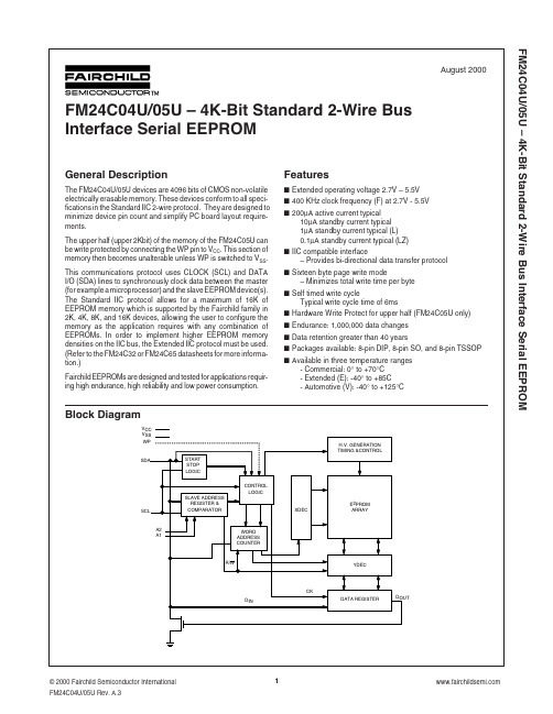
FM24C04U/05U – 4K-Bit Standard 2-Wire Bus Interface Serial EEPROM
Ordering Information FM 24 C XX U F LZ E XXX
Operating Conditions
Ambient Operating Temperature FM24C04U/05U FM24C04UE/05UE FM24C04UV/05UV Positive Power Supply FM24C04U/05U FM24C04UL/05UL FM24C04ULZ/05ULZ 0°C to +70°C -40°C to +85°C -40°C to +125°C 4.5V to 5.5V 2.7V to 5.5V 2.7V to 5.5V
FM24C04U/05U – 4K-Bit Standard 2-Wire Bus Interface Serial EEPROM
Product Specifications Absolute Maximum Ratings
Ambient Storage Temperature All Input or Output Voltages with Respect to Ground Lead Temperature (Soldering, 10 seconds) ESD Rating –65°C to +150°C –0.3V to 6.5V +300°C 2000V min.
元器件交易网
FM24C04U/05U – 4K-Bit Standard 2-Wire Bus Interface Serial EEPROM
74HC02中文资料_数据手册_参数
INPUT nA, nB
UNIT LOADCOEFFICIENT 1.50
AC CHARACTERISTICS FOR 74HCT GND = 0 V; tr = tf = 6 ns; CL = 50 pF
SYMBOL PARAMETER
tPHL/ tPLH tTHL/ tTLH
min.
propagation delay nA, nB to nY
output transition time
Tamb (°C)
74HCT
+25
−40 to+85
typ. max. min. max.
11 19
24
7 15
19
−40 to+125 min. max.
29 22
UNIT
ns ns
TEST CONDITIONS
VCC WAVEFORMS (V)
4.5 Fig.6 4.5 Fig.6
For the DC characteristics see “74HC/HCT/HCU/HCMOS Logic Family Specifications”.
Output capability: standard ICC category: SSI
AC CHARACTERISTICS FOR 74HC GND = 0 V; tr = tf = 6 ns; CL = 50 pF
Quad 2-input NOR gate
Product specification
74HC/HCT02
DC CHARACTERISTICS FOR 74HCT For the DC characteristics see “74HC/HCT/HCU/HCMOS Logic Family Specifications”. Output capability: standard ICC category: SSI
- 1、下载文档前请自行甄别文档内容的完整性,平台不提供额外的编辑、内容补充、找答案等附加服务。
- 2、"仅部分预览"的文档,不可在线预览部分如存在完整性等问题,可反馈申请退款(可完整预览的文档不适用该条件!)。
- 3、如文档侵犯您的权益,请联系客服反馈,我们会尽快为您处理(人工客服工作时间:9:00-18:30)。
12 1-800-735-6200
70
Converter Selection Chart
VI-2
Mechanical Drawing
Features
s Up to 50W/Cubic Inch
s UL, CSA, TÜV, VDE, BABT, AUSTEL
s Up to 90% Efficiency s Size: 4.6" x 2.4" x 0.5"(116,8 x 61,0 x 12,7)
s Remote Sense and Current Limit s OVP, Thermal Shutdown s Logic Disable
s Wide Range Output Adjust
s Compatible Power Booster Modules s ZCS Power Architecture s Low Noise FM Control s CE Marked
VI-200
DC-DC Converters 50 to 200 Watts
Product Highlights
The VI-200 Family, with over 8 million
shipped, is Vicor’s first generation of
“zero-current-switching” component-level DC-DC converters.
Operating at frequencies up to 2 MHz, VI-200 Family Converters offer
exceptional power density, efficiency,noise performance, reliability and ease of use. Power Boosters provide a simple, cost effective, off-the-shelf solution for higher power output requirements. One or more boosters may be used to create synchronous arrays capable of supplying several kilowatts of output power.
The flexibility of Vicor’s power components is also available in half-size, half-power VI-J00 MiniMods. (pg. 72)
Packaging Options
SlimMods™, high power density,
flangeless packages and FinMods™,featuring integral finned heatsinks.SlimMod: Option suffix: - S Example: VI - 2XX - XX - S
FinMod: Option suffix: - F1and - F2Examples:
VI - 2XX - XX -F1, 0.75" height VI - 2XX - XX -F2, 1.00" height
Max. Output For 5V Outputs > 5V Outputs
< 5V Outputs
(1)75W 75W 15A (2)150W 150W 30A (3)
100W
100W
20A
* Brownout 75% of rated load; transient voltage for 1 second.
Max. Output For 5V Outputs > 5V Outputs < 5V Outputs
(4)200W 200W 40A (5)150W 200W 40A (6)
75W
100W
20A
Rev 3 1 of 2
For the latest Vicor Product Information:
12 1-800-735-6200
71
VI-200 E-Grade
VI-200 C-, I-, M-Grade PARAMETER
MIN.TYP.MAX.
MIN.
TYP.
MAX.
UNITS
TEST CONDITIONS
s Input Characteristics Inrush charge
120x10-6120x10-6200x10-6Coulombs
Nominal line
Input reflected ripple current – pp 10%
10%
I IN
Nominal line, full load Input ripple rejection
dB 120 Hz, nominal line dB 2400 Hz, nominal line
No load power dissipation 1.352
1.352
Watts
s Output Characteristics Setpoint accuracy 1%
2%0.5%1%V NOM Load/line regulation 0.5%0.05%0.2%V NOM LL to HL, 10% to Full Load Load/line regulation 1%
0.2%0.5%V NOM LL to HL, No Load to 10%Output temperature drift 0.020.010.02
% / °C Over rated temp.
Long term drift 0.02
0.02%/1K hours
Output ripple - pp: 2V, 3.3V 150 mV 60 mV 100 mV 20 MHz bandwidth 5V 5%2%3%20 MHz bandwidth 10-48V 3%0.75%
1.5%20 MHz bandwidth Trim range 1
50%110%
50%110%Total remote sense compensation 0.5
0.5Volts 0.25V max. neg. leg OVP set point 125%2
115%125%2
135%V NOM Recycle power Current limit
105%135%105%125%I NOM Automatic restart
Short circuit current 320%
140%
20%
130%
I NOM
s Control Pin Characteristics Gate out impedance 5050Ohms Gate in impedance
103103Ohms Gate in open circuit voltage 6
6
Volts Use open collector
Gate in low threshold 0.650.65Volts Gate in low current 66mA
Power sharing accuracy 0.95
1.05
0.95
1.05
s Dielectric Withstand Characteristics Input to output 3,0003,000V RMS Baseplate earthed
Output to baseplate 500500V RMS Input to baseplate 1,5001,500
V RMS
s Thermal Characteristics Efficiency
78-88%80-90%Baseplate to sink 0.20.2°C/Watt With Vicor P/N 01777Thermal shutdown 490
95
10590
95
105
°C
Cool and recycle power (Drivers only)to restart
s Mechanical Specifications Weight
6.0 (170) 6.0 (170)Ounces (Grams)
110V, 12V and 15V outputs, standard trim range ±10%. Consult factory for wider trim range. 2
131% nominal for booster modules.
3Output voltages of 3.3V or 5V incorporate foldback current limiting; all other outputs provide constant current limiting.4No overtemp protection in booster modules.
Converter Specifications
(typical at T BP =25°C, nominal line and 75% load, unless otherwise specified)
25+20Log ( Vin
)
Vout
30+20Log ( Vin
)Vout
20+20Log ( Vin
)
Rev 3 2 of 2
For the latest Vicor Product Information: 。