302A10879X;中文规格书,Datasheet资料
302-AW-135中文资料
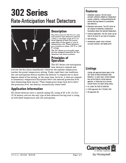
302 Series CS-2519 09/01/06Page 1 of 2Features•Immediate response. The 302 Seriesactivates whenever ambient air temperature reaches a detector's setting,eliminating the thermal time lag inherent in conventional heat detectors.•Eliminates false alarms. The 302 Series do not respond to momentary temperaturefluctuations below the selected temperature.•Universal application. The 302 Series can be used in all areas for any type of occupancy.•Self-restoring.•Hermetically sealed, shock resistant,corrosion resistant, and tamper-proff.ListingsListings and approvals below apply to the 302 Series M Rate-Anticipation Heat Detectors. In some cases, certain modules may not be listed by certain approval agencies, or listing may be in process.Consult factory for latest listing status.•UL Listed: file S539 & E35018A.•CSFM approved: file 7270-0021:001.•FM approved: file302 SeriesRate-Anticipation Heat DetectorsDescriptionThe Thermotech 302 Series rate-anticipation heat detectors operate within a conrolled range of two to three degrees of their set points,regardless of the speed or rate of temperature rise. These detectors are available in either 135° F or 194°F ratings.The 302 Series are normally-open devices designed especially for fire detection and alarm systems.Principles of OperationThe 302 Series rate-anticipation heat detectors respond andactivate the fire alarm immediately whenever the ambient temperature reaches the preset temperature setting. Under rapid heat rise conditions,the rate-anticipation feature enables the detector to respond one to three degrees ahead of the setting. At the same time, however, it does not respond to momentary temperature flucuations below the selected protection level,thus eliminating false alarms. When temperature drops back down below the protection level, the detector automatically resets itself.Application Information302 Series detectors have a smooth-ceiling UL rating of 50' x 50' (15.24 x 15.24 meters) and are the only type of heat detectors having such a rating on both fixed temperature and rate anticipation.6935p h o 1.j p g302 Series CS-2519 09/01/06Page 2 of 2Specifications and wiring information are provided for information only and are believed to be accurate. Gamewell-FCI assumes no responsibility for their use.Data and design are subject to change without notice. Installation and wiring instructions shipped with the product shall always be used for actual installation.For more information, contact Gamewell-FCI.Gamewell-FCI 12 Clintonville Road Northford, CT 06472-1610Phone: 203-484-7161Fax: A Honeywell Company © 2006 Gamewell-FCISpecificationsDimensionsTotal overall length: 4-1/8"Base diameter: 2"Electrical Ratings Voltage Current 6-125 VAC 5 amps 6-25 VDC 1 amp 125 VDC0.5 ampProduct Line Information302-135: 135°F Interior Vertical Mounting, FM and UL (See Note 1).302-194: 194°F Interior Vertical Mounting, FM and UL (See Note 1).302-AW-135:135°F All-Weather Vertical Mounting, FM and UL (See Note 2).302-AW-194: 194°F All-Weather Vertical Mounting, FM and UL (See Note 2).302-ET-135:135°F All-Weather Vertical Mounting, FM and UL (See Note 3).302-ET-194: 194°F All-Weather Vertical Mounting, FM and UL (See Note 3).302-EPM-135: 135°F Explosion-Proof Mounting, UL (See Note 4).302-EPM-194: 194°F Explosion Proof Mounting, UL (See Note 4).AP-P : Decorative white plastic adaptor plate for mounting 302 and 302-AM to 4"outlet box.Note 1: For interior mounting in any atmosphere that is compatible with termi-nal screw type connections. UL rating 50' x 50' (15.24 x 15.24 meters).Note 2: Humitically sealed for moisture-proof or dust-proof installations. Requires no special backbox when the all-weather leads are properly spliced to 'THW' or equivalent type wire.Note 3: Humitically sealed for moisture-proof or dust-proof installations. Requires no special backbox. Has plastic hexagonal wrench grip bushing with 1/2" (1.27 cm)conduit threads for attachment to threaded hub cover, or any special outlet box.Note 4: Explosion-proof for installation in hazardous locations. Has hexagonal wrench grip bushing with 1/2" (1.27 cm) conduit threads for attachment to threaded hub cover of Series JL fixture fitting as manufactured by Killark Electric Co., or equal.FINE SILVERCONTACT POINTS EXPANSION STRUTS HIGH EXPANSIONSENSING SHELL 0.040ANODIZED ALUMINUM HEAT ANTICIPATION CONTROL SLEEVE SETTING SCREWDEVCONHERMETIC SEALCut-Away View。
ATSTK520;中文规格书,Datasheet资料

STK520 .............................................................................................. User GuideSTK520 User Guide 3Table of ContentsSection 1Introduction............................................................................................1-2Section 2Using the STK520 Top Module.............................................................2-42.1Connecting the STK520 to the STK500 Starter Kit..................................2-42.1.1Placing an AT90PWM3 on the STK520.............................................2-42.1.2Placing an AT90PWM2 on the STK520.............................................2-52.2Programming the AVR..............................................................................2-72.2.1In-System Programming....................................................................2-72.2.2High-voltage Programming................................................................2-82.3JTAGICE mkII Connector.........................................................................2-92.4STK520 Jumpers, Leds & Test Points....................................................2-112.5DALI Interface.........................................................................................2-122.6Potentiometer.........................................................................................2-13Section 3Troubleshooting Guide........................................................................3-14Section 4Technical Specifications......................................................................4-16Section 5Technical Support ...............................................................................5-17Section 6Complete Schematics .........................................................................6-20IntroductionSection 1IntroductionThe STK520 board is a top module designed to add AT90PWM family support to theSTK500 development board from Atmel Corporation.The STK520 includes connectors and hardware allowing full utilization of the new fea-tures of the AT90PWM, while the Zero Insertion Force (ZIF) socket allows easy to use ofSO24 & SO32 packages for prototyping.This user guide acts as a general getting started guide as well as a complete technicalreference for advanced users.Notice that in this guide, the word AVR is used to refer to the target component(AT90PWM2, AT90PWM3...)Figure 1-1. STK520 Top Module for STK500Introduction1.1Features STK520 is a New Member of the Successful STK500 Starter Kit Family.Supports the AT90PWM2 & AT90PWM3.DALI Hardware Interface.Supported by AVR Studio® 4.Zero Insertion Force Socket for SO24 & SO32 Packages.High Voltage Parallell Programming.Serial Programming.DALI Peripherals can be Disconnected from the Device.6 Pin Connector for On-chip Debugging using JTAG MKII Emulator.Potentiometer for the Demo Application.Quick Reference to all Switches and Jumpers in the Silk-Screen of the PCB.Using the STK520 Top Module Section 2Using the STK520 Top Module2.1Connecting the STK520 to theSTK500 Starter Kit Connect the STK520 to the STK500 expansion header 0 and 1. It is important that the top module is connected in the correct orientation as shown in Figure 2-1. The EXPAND0 written on the STK520 top module should match the EXPAND0 written beside the expansion header on the STK500 board.Figure 2-1. Connecting STK520 to the STK500 BoardNote:Connecting the STK520 with wrong orientation may damage the board.2.1.1Placing anAT90PWM3 on theSTK520The STK520 contains both a ZIF socket for a SO32 package. Care should be taken so that the device is mounted with the correct orientation. Figure 2-2 shows the location of pin1 for the ZIF socket.Using the STK520 Top ModuleFigure 2-2. Pin1 on ZIF SocketCaution: Do not mount an AT90PWM3 on the STK520 at the same time as an AVR ismounted on the STK500 board or at the same time as an AT90PWM2 is mounted on theSTK520 board. None of the devices might work as intended.2.1.2Placing anAT90PWM2 on theSTK520The STK520 contains both a ZIF socket for a SO24 package. Care should be taken so that the device is mounted with the correct orientation. Figure 2-2 shows the location of pin1 for the ZIF socket.Figure 2-3. Pin1 on ZIF SocketPIN1PIN1Using the STK520 Top Module Caution: Do not mount an AT90PWM2 on the STK520 at the same time as an AVR is mounted on the STK500 board or at the same time as an AT90PWM3 is mounted on the STK520 board. None of the devices might work as intended.Using the STK520 Top Module2.2Programming theAVR The AVR (AT90PWM2, AT90PWM3...) can be programmed using both SPI and High-voltage Parallel Programming. This section will explain how to connect the programming cables to successfully use one of these two modes. The AVR Studio STK500 software is used in the same way as for other AVR partsNote:The AT90PWM3 also support Self Programming, See AVR109 application note for more information on this topic.2.2.1In-SystemProgramming Figure 2-4. In-System ProgrammingTo program the AT90PWM3 using ISP Programming mode, connect the 6-wire cable between the ISP6PIN connector on the STK500 board and the ISP connector on the STK520 board as shown in Figure 2-4. The device can be programmed using the Serial Programming mode in the AVR Studio4 STK500 software.Note:See STK500 User Guide for information on how to use the STK500 front-end software for ISP Programming.Using the STK520 Top Module2.2.2High-voltageProgramming Figure 2-5. High-voltage (Parallel) ProgrammingTo program the AVR using High-voltage (Parallel) Programming, connect the PROGC-TRL to PORTD and PROGDATA to PORTB on the STK500 as shown in Figure 2-5. Make sure that the TOSC-switch is placed in the XTAL position.As described in the STK500 User Guide (jumper settings), mount the BSEL2 jumper in order to High-voltage Program the ATmega devices. This setting also applies to High-voltage Programming of the AVR.The device can now be programmed using the High-voltage Programming mode in AVR Studio STK500 software.Note:See the STK500 User Guide for information on how to use the STK500 front-end software in High-voltage Programming mode.Note:For the High-voltage Programming mode to function correctly, the target voltage must be higher than 4.5V.Using the STK520 Top Module2.3JTAGICE mkIIConnector See the following document :“JTAGICE mkII Quick Start Guide” which purpose is “Connecting to a target board with the AVR JTAGICE mkII”.This note explains which signals are required for ISP and which signals are required for debugWIRE.Figure 2-6 shows how to connect the JTAGICE mkII probe on the STK520 board. Figure 2-6. Connecting JTAG ICE to the STK520The ISP connector is used for the AT90PWM3 built-in debugWire interface. The pin out of the connector is shown in Table 2-1 and is compliant with the pin out of the JTAG ICE available from Atmel. Connecting a JTAG ICE to this connector allows On-chip Debug-ging of the AT90PWM3.More information about the JTAG ICE and On-chip Debugging can be found in the AVR JTAG ICE User Guide, which is available at the Atmel web site, .分销商库存信息: ATMELATSTK520。
BLF175,112;中文规格书,Datasheet资料
• Easy power control
• Good thermal stability
ook, halfpage
• Withstands full load mismatch
1
4
• Gold metallization ensures
excellent reliability.
d
DESCRIPTION
PINNING - SOT123A
PIN
DESCRIPTION
1 drain
2 source
3 gate
4 source
WARNING
Product and environmental safety - toxic materials
This product contains beryllium oxide. The product is entirely safe provided that the BeO disc is not damaged. All persons who handle, use or dispose of this product should be aware of its nature and of the necessary safety precautions. After use, dispose of as chemical or special waste according to the regulations applying at the location of the user. It must never be thrown out with the general or domestic waste.
Silicon N-channel enhancement mode vertical D-MOS transistor designed for large signal amplifier applications in the HF/VHF frequency range.
SSCUB-200A;中文规格书,Datasheet资料
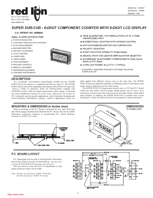
U.S. PATENT NO. 4599600IDEAL IN APPLICATIONS FOR:O POSITION INDICATIONO COUNTING FROM MULTIPLE SOURCES O FLOW MEASUREMENTO MACHINE MONITORSO SECURITY EQUIPMENTO UTILITY METERSO COMPUTERSO VIDEO GAMESO TEST EQUIPMENTO MACHINE CONTROLSO MEDICAL EQUIPMENTO DISPENSING EQUIPMENTO PORTABLE INSTRUMENTS O TRUE QUADRATURE - WITH RESOLUTIONS UP TO 4 TIMES THE ENCODED INPUTO BI-DIRECTIONAL COUNTING WITH UP/DOWN CONTROLO ANTI-COINCIDENCE ADDITION AND SUBTRACTIONO POLARITY INDICATIONO8-DIGIT COUNTING CAPABILITY(6-digit display)O DECIMAL POINT AND LEADING ZERO BLANKING SELECTION O SOLDERLESS, ELASTOMERIC INTERCONNECTS (Snap mounts directly on P.C. board)O ULTRA LOW POWER, 25 µA AT 5 V (TYPICAL)*ACCESSORY HARDWARE AVAILABLE FOR PANEL MOUNTINGSUPER SUB-CUBSUPER SUB-CUB - 8-DIGIT COMPONENT COUNTER WITH 6-DIGIT LCD DISPLAYP.C. BOARD LAYOUTP.C. Board pads may be gold or tin-lead plated. Pad surface must be flat without excessive tin-lead build-up. (Layout views are from SUPER SUB-CUB mounting side of board.)Pad area must be clean and free of contaminants so that proper electrical contact can be made.Note: All hole size tolerances ±0.003" (0.08 mm)All other tolerances ±0.005" (0.13 mm)CAUTIONThis device contains CMOS circuitry which requires special anti-static handling to the same degree required by standard CMOS integrated circuits.Units should be stored in the conductive packaging used to ship the devices.Containers should be opened and units handled only on a conductive table top by personnel wearing wrist strap grounding equipment. These devices have the same protection circuits as standard CMOS devices to prevent damage to inputs due to nominal over-voltage.RATINGSYMBOLVALUEUNITDC Supply VoltageV DD -0.5 to +6.5VDC Input Voltage, All Inputs V I -0.5 to (V DD +.5)VDC Operating Temperature T A -35 to +85°C Storage TemperatureT STG-35 to +85°CMAXIMUM RATINGS (VOLTAGE REF. TO V SS )SYMBOL PARAMETER MIN.TYP .MAX.UNIT TEST CONDITION V DD Supply Voltage 2.5 6.0VDC All Modes Except4.56.0Anti-Coincidence Modes Supply Current 2540µA F C =10 KHz I DD Supply Current 60100µA F C =10 KAnti-Coincidence Modes I DDQ Quiescent Current 1016µA Not CountingV IH Input High Voltage 3.93.0VDC V IL Input Low Voltage 0.90.5VDC I ILInput Leakage Current 0.010.1µA V SS <V IN <V DD400KHz X1, -10 & 100 Bidirectional Modes Count Frequency 250KHz X2, -5 & 50 Bidirectional Modesfc max(50% Duty Cycle)200KHz X1, X2, -10, 100, 5 & 50 Quad. Mode 100KHz X4, -2.5 & 25 Quadrature Mode 20KHz Anti-Coincidence Modes fosc Oscillator Frequency 240Hz R EXT = 2.4MT RSTReset Pulse Width10µSELECTRICAL CHARACTERISTICS V DD = 5 V ±10% @ 20°C UNLESS OTHERWISE SPECIFIEDBI-DIRECTIONAL COUNTING MODESFor Bi-Directional counting, input “A”serves as the count input, while input “B”serves as the direction control input. In the Times 1 Mode when “B”is at a low level, a negative going transition at “A”will cause the counter to count in the positive direction. When “B”is at a high level, a negative going transition at “A”will cause the counter to count in the negative direction.TABLE I illustrates the level settings of the Mode Select Inputs for the various modes of Bi-Directional counting. The Times 2 Mode works like Times 1 Mode except the counter changes on a positive going transition at “A”, as well as on a negative going transition at “A”. There are also two Divide-By Modes which prescale the display by 10 or by 100. This results in the capability of displaying the 7th and 8th digit of the internal counter. (Along with Times 2, this gives an MODES OF OPERATIONANTI-COINCIDENCE SUMMING MODESFor Anti-Coincidence Summing, input “A”and input “B”both serve as Add Inputs. These modes effectively separate count pulses which may simultaneously occur at the two inputs. The unit then processes the count pulses into a string of time-separated pulses so that the internal counter will not lose any counts. Both inputs respond to the negative going transition in the Times 1 Mode.TABLE III illustrates the level settings of the Mode Select Inputs for the various modes of Anti-Coincidence Summing.Note: The maximum count rate for all Anti-Coincidence counting modes is 20KHz.TABLE IIITYPICAL APPLICATIONSPANEL BEZEL KIT FOR THE SUPER SUB-CUB P/N HWK50000)This kit provides a convenient way to adapt the SUPER SUB-CUB for panel mounting. The kit includes the black plastic bezel, the panel and internal window gaskets, P.C. Board, 12" ribbon cableand mounting screws.TYPICALAPPLICATIONS (CONT'd)DIMENSIONS & PANEL CUT-OUT In inches (mm)ORDERING INFORMATIONSUPER SUB-CUB PROTOTYPING BOARDThis board is a handy way of doing experimental and prototyping work with the SUPER SUB-CUB.It easily plugs into standard 0.1" spacing bread boards. This in turn, greatly simplifies bread board work.SUPER SUB-CUB PROTO TYPING BOARDP/N DMOSCBO3This page intentionally left blankLIMITED WARRANTYThe Company warrants the products it manufactures against defects in materials and workmanship for a period limited to two years from the date of shipment, provided the products have been stored, handled, installed, and used under proper conditions. The Company’s liability under this limited warranty shall extend only to the repair or replacement of a defective product, at The Company’s option. The Company disclaims all liability for any affirmation, promise or representation with respect to the products.The customer agrees to hold Red Lion Controls harmless from, defend, and indemnify RLC against damages, claims, and expenses arising out of subsequent sales of RLC products or products containing components manufactured by RLC and based upon personal injuries, deaths, property damage, lost profits, and other matters which Buyer, its employees, or sub-contractors are or may be to any extent liable, including without limitation penalties imposed by the Consumer Product Safety Act (P.L. 92-573) and liability imposed upon any person pursuant to the Magnuson-Moss Warranty Act (P.L. 93-637), as now in effect or as amended hereafter.No warranties expressed or implied are created with respect to The Company’s products except those expressly contained herein. The Customer acknowledges the disclaimers and limitations contained herein and relies on no other warranties or affirmations.Red Lion Controls20 Willow Springs Circle York PA 17406Tel +1 (717) 767-6511 Fax +1 (717) 764-0839Red Lion Controls APUnit 101, XinAn PlazaBuilding 13, No.99 Tianzhou RoadShangHai, P.R. China 200223Tel +86 21 6113-3688Fax +86 21 6113-3683 Red Lion Controls BVPrinterweg 10NL - 3821 AD AmersfoortTel +31 (0) 334 723 225Fax +31 (0) 334 893 793分销商库存信息: RED-LION-CONTROLS SSCUB-200/A。
AO8822;中文规格书,Datasheet资料
Symbolt ≤ 10s Steady-State Steady-StateR θJLW Maximum Junction-to-Lead°C/W°C/W Maximum Junction-to-Ambient A D 6413083Maximum Junction-to-Ambient A T A =25°C T A =70°C Power DissipationBPulsed Drain Current CContinuous Drain T A =25°C AV Units ParameterAbsolute Maximum Ratings T A =25°C unless otherwise notedV Gate-Source Voltage Drain-Source Voltage °C/W R θJA 6310183°CThermal Characteristics Units ParameterTyp Max T A =70°CJunction and Storage Temperature Range Pin 1DSSymbolMin Typ Max Units BV DSS 20VV DS =20V, V GS =0V1T J =55°C 5I GSS 10µA BV GSO ±12V V GS(th)Gate Threshold Voltage 0.50.81V I D(ON)30A 131518T J =125°C2227151722m Ω161823m Ω182127m Ω28m Ωg FS 31S V SD 0.71V I S2A C iss 520650780pF C oss 140pF C rss60pFQ g (10V)121518nC Q g (4.5V)56.78nC Q gs 3.6nC Q gd 3nC t D(on)0.25us t r 0.45us t D(off)11us t f 4ust rr 81012ns Q rr81113.5nCTHIS PRODUCT HAS BEEN DESIGNED AND QUALIFIED FOR THE CONSUMER MARKET. APPLICATIONS OR USES AS CRITICAL COMPONENTS IN LIFE SUPPORT DEVICES OR SYSTEMS ARE NOT AUTHORIZED. AOS DOES NOT ASSUME ANY LIABILITY ARISING OUT OF SUCH APPLICATIONS OR USES OF ITS PRODUCTS. AOS RESERVES THE RIGHT TO IMPROVE PRODUCT DESIGN,FUNCTIONS AND RELIABILITY WITHOUT NOTICE.Body Diode Reverse Recovery TimeDrain-Source Breakdown Voltage On state drain currentI D =250µA, V GS =0V V GS =10V, V DS =5V V GS =10V, I D =7AReverse Transfer CapacitanceI F =7A, dI/dt=500A/µsV GS =0V, V DS =10V, f=1MHzSWITCHING PARAMETERS Electrical Characteristics (T J =25°C unless otherwise noted)STATIC PARAMETERS ParameterConditions I DSS µA V DS =V GS I D =250µA V DS =0V, V GS = ±10V Zero Gate Voltage Drain Current Gate-Body leakage current Gate-Source Breakdown Voltage V DS =0V, I G =±250µA Forward Transconductance Diode Forward VoltageR DS(ON)Static Drain-Source On-Resistancem ΩI S =1A,V GS =0VV DS =5V, I D =7A V GS =1.8V, I D =2AV GS =4.5V, I D =6.6A V GS =3.6V, I D =6A V GS =2.5V, I D =5.5A Turn-Off Fall TimeTotal Gate Charge V GS =10V, V DS =10V, I D =7AGate Source Charge Gate Drain Charge Total Gate Charge Body Diode Reverse Recovery Charge I F =7A, dI/dt=500A/µsMaximum Body-Diode Continuous CurrentInput Capacitance Output CapacitanceTurn-On DelayTime DYNAMIC PARAMETERS Turn-On Rise Time Turn-Off DelayTime V GS =10V, V DS =10V, R L =1.5Ω,R GEN =3ΩA. The value of R θJA is measured with the device mounted on 1in 2FR-4 board with 2oz. Copper, in a still air environment with T A =25°C. The value in any given application depends on the user's specific board design.B. The power dissipation P D is based on T J(MAX)=150°C, using ≤ 10s junction-to-ambient thermal resistance.C. Repetitive rating, pulse width limited by junction temperature T J(MAX)=150°C. Ratings are based on low frequency and duty cycles to keep initialT J =25°C.D. The R θJA is the sum of the thermal impedence from junction to lead R θJL and lead to ambient.E. The static characteristics in Figures 1 to 6 are obtained using <300µs pulses, duty cycle 0.5% max.F. These curves are based on the junction-to-ambient thermal impedence which is measured with the device mounted on 1in 2 FR-4 board with 2oz. Copper, assuming a maximum junction temperature of T J(MAX)=150°C. The SOA curve provides a single pulse ratin g.TYPICAL ELECTRICAL AND THERMAL CHARACTERISTICSTYPICAL ELECTRICAL AND THERMAL CHARACTERISTICSQ g (nC)Figure 7: Gate-Charge CharacteristicsV G S (V o l t s )48121620V DS (Volts)Figure 8: Capacitance Characteristics C a p a c i t a n c e (p F )VdsCharge Gate Charge Test Circuit & WaveformD iode RVVddVddVR esistive S w itching Test C ircuit & W aveform s分销商库存信息: AOSAO8822。
2KAX原厂中文规格书
Rev. 1.1
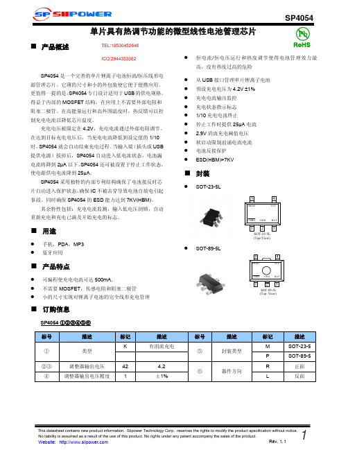
■ 功能框图
SP4054
■ 电学特性参数
输入电压
参数
输入电流
输出控制电压
BAT端电流
涓流充电电流
标号 Vcc Icc Vfloat
Ibat
Itrikl
条件
Charge mode,Rprog=10K Standby mode Shutdown mode(Rprog not connected,Vcc<Vbat or Vcc<Vuv) 0℃<TA<85℃, IBAT = 40mA Rprog=10k,Current mode Rprog=2k,Current mode Standby mode,Vbat=4.2V Shutdown mode Battery reverse mode, VBAT=-4V Sleep mode,Vcc=0V Vbat<Vtrikl,Rprog=2k
■ 封装
SOT-23-5L
5
4
PROG
VCC
SOT-89-5L
CHRG GND BAT
12 3
SOT-23-5L (Top View)
5
4
PROG PROG
VCC
CHRG GND BAT
1 23 1 SOT-829-5L 3
(Top View)
SP4054 ①②③④⑤⑥
标号 ① ②③ ④
描述 类型
Rev. 1.1
涓流充电极限电压 涓流充电迟滞电压 电源低电闭锁阈值电压 电源低电阈值电压迟滞电压 手动关闭阈值电压
Vcc-Vbat停止工作阈值电压
C/10 终端阈值电流 PROG端电压 CHRG端弱下拉电流 CHRG端最小输出电压 电池再充电迟滞电压
通华芯微电子 THX203H开关电源 控制器集成电路 参数表说明书

THXTHXTHXTHXTHXTHXTHXTHXTHXTHXTHXTHXTHXTHXTHXTHXTHXTHXTHXTHXTHXTHXTHX器件参数表 DataSheetTHXTHXTHXTHXTHXTHXTHXTHXTHXTHXTHXTHXTHXTHXTHXTHXTHXTHXTHXTHXTHXTHXTHX发行日期:2006.9.1文档编号:SPEC203H0609A1THX203H【开关电源控制器集成电路】THX Micro-elec. 通 华 芯 微 电 子THXTHXTHXTHXTHXTHXTHXTHXTHXTHXTHXTHXTHXTHXTHXTHXTHXTHX版本历史日期版本说明修订版本2006.9.1 第一版James A目录概述、特点、应用领域 (3)内部电路参考框图 (4)引脚功能描述 (4)极限参数 (5)推荐工作条件 (5)电气参数 (5)原理描述 (7)电参数定义 (8)应用信息 (9)典型应用电路 (11)元器件清单 (12)变压器绕制 (13)测试数据 (14)主要测试点波形 (15)热阻与结温参数 (19)封装尺寸图 (20)联系信息 (21)概述高性能电流模式PWM控制器。
专为高性价比AC/DC转换器设计。
在85V-265V的宽电压范围内提供高达12W的连续输出功率,峰值输出功率更可达18W。
优化的高合理性的电路设计结合高性能价格比的双极型制作工艺,最大程度上节约了产品的整体成本。
该电源控制器可工作于典型的反激电路拓扑中,构成简洁的AC/DC转换器。
IC内部的启动电路被设计成一种独特的电流吸入方式,可利用功率开关管本身的放大作用完成启动,这显著地降低了启动电阻的功率消耗;而在输出功率较小时IC将自动降低工作频率,从而实现了极低的待机功耗。
在功率管截止时,内部电路将功率管反向偏置,直接利用了双极性晶体管的CB高耐压特性,大幅提高功率管的耐电压能力直到700V的高压,这保证了功率管的安全。
HT862_Datasheet技术文档规格书

此外,HT862内部集成免滤波器调制技术,能够 直接驱动扬声器,内置的关断功能使待机电流最小 化,还集成了输出端过流保护、片内过温保护和电源 欠压异常保护等功能。
・保护功能:过流/过热/欠压异常保护功能
・无铅无卤封装,TSSOP20L-PP
典型特性曲线.........................................................................................................................................11 AGC ......................................................................................................................................................11 BOOST + Class D ............................................................................................................................... 13
使输出音频信号限制在固定失真水平内
・内置自适应同步升压 - 小音乐信号时不升压,可大幅提高系统效率,延 长电池续航时间 - 外围无需二极管
・内置自动限温控制功能 -特别适用于升压8.5V+D类,升压+AB类状态下及
环境温度较高的情况,显著提升音乐峰值功率
- 1、下载文档前请自行甄别文档内容的完整性,平台不提供额外的编辑、内容补充、找答案等附加服务。
- 2、"仅部分预览"的文档,不可在线预览部分如存在完整性等问题,可反馈申请退款(可完整预览的文档不适用该条件!)。
- 3、如文档侵犯您的权益,请联系客服反馈,我们会尽快为您处理(人工客服工作时间:9:00-18:30)。
- 55 °C to + 125 °C 15 pos. 26 pos. 44 pos. 62 pos. 78 pos. ≤ 50 N ≤ 84 N ≤ 120 N ≤ 70 N ≤ 200 N
Quality class
A = Quality class 3 = 50 mating cycles B = Quality class 2 = 200 mating cycles C = Quality class 1 = 500 mating cycles
分销商库存信息:
CONEC 302A10879X
D-Subminiature, Standard 9, 15, 25, 37 and 50 position
D-Subminiature, High Density 15, 26, 44, 62 and 78 position
Polyester GF UL94 V-0 CU alloy Gold plated over nickel Steel tin plated brass tin plated stainless steel
Insulation resistance Clearance and creepage distance
Operating temperature Mating and unmating forces 9 pos. 15 pos. 25 pos. 37 pos. 50 pos. ≤ 30 N ≤ 50 N ≤ 83 N ≤ 123 N ≤ 167 N
15 pos.
62 pos.
26 pos.
ห้องสมุดไป่ตู้
78 pos.
44 pos.
PCB layout Kat1iU1A (View: component side)
/
1| 17
D-S U B Co n n e c t o r s
PCB layout, D-SUB High Density
Technical alterations are subject to change without notice.
/
1| 3
D-SUB C o n n e c t o r s
PCB layout, D-SUB High Density
Solder pin, angled – .350" 7.98 mm – Socket connector
D-S U B Co n n e c t o r s
Mating conditions
Float mount tolerance guide
Rigid mount vertical to tolerance guide
Rigid mount tolerance guide
Panel cut-out
Rear panel mounting Front panel mounting
Mechanical and electrical characteristics
Test voltage U eff NN Working voltage 1000 V 125 V ≈ 60 V ≈ Depending on isolation coordination (refer to DIN VDE 0110 IEC 664-1) 7,5 A (UL) 5 A (CSA,VDE) 3 A (UL,VDE) 2,5 A (CSA)
Solder pin, angled – .350" 7.98 mm – Plug connector
15 pos.
62 pos.
26 pos.
78 pos.
44 pos.
PCB layout Kat1iU2A (View: component side)
1| 18 /
Shell size
9 15 25 37 50 15 26 44 62 78
A ± 0,13
20.50 28.80 42.50 59.10 56.30
B ± 0,13
22.20 30.50 44.30 60.70 61.10
C ± 0,13
25.00 33.30 47.04 63.50 61.10
D ± 0,13
Current rating Contact resistance
Max. 10 mΩ prior to stressing, Δ R max. 10 mΩ after stressing per DIN 41652, Part 2 ≥5 GΩ Contact – contact Contact – earth ≥ .004" 1.0 mm ≥ .047“ 1.2 mm ≥ .024“ 0,6 mm
11.40 11.40 11.40 11.40 11.40
E ± 0,13
13.00 13.00 13.00 13.00 15.80
1| 2/
D-SUB C o n n e c t o r s
Technical Data
Materials
Insulator Contacts Contact plating Shell