MAX1237EUA+;MAX1236EUA+;MAX1238EEE+;MAX1239EEE+;MAX1239KEEE+;中文规格书,Datasheet资料
MAX系列芯片大全

MAXIM/DALLAS 中文数据资料DS12CR887, DS12R885, DS12R887 RTC,带有恒压涓流充电器DS1870 LDMOS RF功放偏置控制器DS1921L-F5X Thermochron iButtonDS1923 温度/湿度记录仪iButton,具有8kB数据记录存储器DS1982, DS1982-F3, DS1982-F5 1k位只添加iButton?DS1990A 序列号iButtonDS1990R, DS1990R-F3, DS1990R-F5 序列号iButtonDS1991 多密钥iButtonDS2129 LVD SCSI 27线调节器DS2401 硅序列号DS2406 双通道、可编址开关与1k位存储器DS2408 1-Wire、8通道、可编址开关DS2411 硅序列号,带有VCC输入DS2413 1-Wire双通道、可编址开关DS2430A 256位1-Wire EEPROMDS2431 1024位、1-Wire EEPROMDS2480B 串行、1-Wire线驱动器,带有负荷检测DS2482-100 单通道1-Wire主控制器DS2482-100 勘误表PDF: 2482-100A2DS2482-800, DS2482S-800 八通道1-Wire主控制器DS2482-800 勘误表PDF: 2482-800A2DS2502 1k位只添加存储器DS2505 16k位只添加存储器DS28E04-100 4096位、可寻址、1-Wire EEPROM,带有PIODS3170DK DS3/E3单芯片收发器开发板DS3231, DS3231S 高精度、I2C集成RTC/TCXO/晶振DS33Z44 四路以太网映射器DS3902 双路、非易失、可变电阻器,带有用户EEPROMDS3906 三路、非易失、小步长调节可变电阻与存储器DS3984 4路冷阴极荧光灯控制器DS4302 2线、5位DAC,提供三路数字输出DS80C400-KIT DS80C400评估套件DS80C410, DS80C411 具有以太网和CAN接口的网络微控制器DS80C410 勘误表PDF: 80C410A1DS89C430, DS89C440, DS89C450 超高速闪存微控制器DS89C430 勘误表PDF: 89C430A2DS89C440 勘误表PDF: 89C440A2DS89C450 勘误表PDF: 89C450A2DS89C430 勘误表PDF: 89C430A3DS89C440 勘误表PDF: 89C440A3DS89C450 勘误表PDF: 89C450A3DS89C430 勘误表PDF: 89C430A5DS89C440 勘误表PDF: 89C440A5DS89C450 勘误表PDF: 89C450A5DS9090K 1-Wire器件评估板, B版DS9097U-009, DS9097U-E25, DS9097U-S09 通用1-Wire COM端口适配器DS9490, DS9490B, DS9490R USB至1-Wire/iButton适配器MAX1034, MAX1035 8/4通道、±VREF多量程输入、串行14位ADCMAX1072, MAX1075 1.8Msps、单电源、低功耗、真差分、10位ADCMAX1076, MAX1078 1.8Msps、单电源供电、低功耗、真差分、10位ADC,内置电压基准MAX1146, MAX1147, MAX1148, MAX1149 多通道、真差分、串行、14位ADCMAX1149EVKIT MAX1149评估板/评估系统MAX1220, MAX1257, MAX1258 12位、多通道ADC/DAC,带有FIFO、温度传感器和GPIO端口MAX1224, MAX1225 1.5Msps、单电源、低功耗、真差分、12位ADCMAX1258EVKIT MAX1057, MAX1058, MAX1257, MAX1258评估板/评估系统MAX1274, MAX1275 1.8Msps、单电源、低功耗、真差分、12位ADCMAX13000E, MAX13001E, MAX13002E, MAX13003E, MAX13004E, MAX13005E 超低电压电平转换器MAX1302, MAX1303 8/4通道、±VREF多量程输入、串行16位ADCMAX1304, MAX1305, MAX1306, MAX1308, MAX1309, MAX1310, MAX1312, MAX1313,MAX1314 8/4/2通道、12位、同时采样ADC,提供±10V、±5V或0至+5V模拟输入范围MAX13050, MAX13052, MAX13053, MAX13054 工业标准高速CAN收发器,具有±80V故障保护MAX13080E, MAX13081E, MAX13082E, MAX13083E, MAX13084E, MAX13085E, MAX13086E, MAX13087E, MAX13088E, MAX13089E +5.0V、±15kV ESD保护、失效保护、热插拔、RS-485/RS-422收发器MAX13101E, MAX13102E, MAX13103E, MAX13108E 16通道、带有缓冲的CMOS逻辑电平转换器MAX1334, MAX1335 4.5Msps/4Msps、5V/3V、双通道、真差分10位ADCMAX1336, MAX1337 6.5Msps/5.5Msps、5V/3V、双通道、真差分8位ADCMAX13481E, MAX13482E, MAX13483E ±15kV ESD保护USB收发器, 外部/内部上拉电阻MAX1350, MAX1351, MAX1352, MAX1353, MAX1354, MAX1355, MAX1356, MAX1357 双路、高端、电流检测放大器和驱动放大器MAX1450 低成本、1%精确度信号调理器,用于压阻式传感器MAX1452 低成本、精密的传感器信号调理器MAX1487, MAX481, MAX483, MAX485, MAX487, MAX488, MAX489, MAX490, MAX491 低功耗、限摆率、RS-485/RS-422收发器MAX1492, MAX1494 3位半和4位半、单片ADC,带有LCD驱动器MAX1494EVKIT MAX1493, MAX1494, MAX1495评估板/评估系统MAX1497, MAX1499 3位半和4位半、单片ADC,带有LED驱动器和μC接口MAX1499EVKIT MAX1499评估板/评估系统MAX15000, MAX15001 电流模式PWM控制器, 可调节开关频率MAX1515 低电压、内置开关、降压/DDR调节器MAX1518B TFT-LCD DC-DC转换器, 带有运算放大器MAX1533, MAX1537 高效率、5路输出、主电源控制器,用于笔记本电脑MAX1533EVKIT MAX1533评估板MAX1540A, MAX1541 双路降压型控制器,带有电感饱和保护、动态输出和线性稳压器MAX1540EVKIT MAX1540评估板MAX1551, MAX1555 SOT23、双输入、USB/AC适配器、单节Li+电池充电器MAX1553, MAX1554 高效率、40V、升压变换器,用于2至10个白光LED驱动MAX1556, MAX1557 16μA IQ、1.2A PWM降压型DC-DC转换器MAX1556EVKIT MAX1556EVKIT评估板MAX1558, MAX1558H 双路、3mm x 3mm、1.2A/可编程电流USB开关,带有自动复位功能MAX1586A, MAX1586B, MAX1586C, MAX1587A, MAX1587C 高效率、低IQ、带有动态内核的PMIC,用于PDA和智能电话MAX16801A/B, MAX16802A/B 离线式、DC-DC PWM控制器, 用于高亮度LED驱动器MAX1858A, MAX1875A, MAX1876A 双路180°异相工作的降压控制器,具有排序/预偏置启动和POR MAX1870A 升/降压Li+电池充电器MAX1870AEVKIT MAX1870A评估板MAX1874 双路输入、USB/AC适配器、1节Li+充电器,带OVP与温度调节MAX1954A 低成本、电流模式PWM降压控制器,带有折返式限流MAX1954AEVKIT MAX1954A评估板MAX19700 7.5Msps、超低功耗模拟前端MAX19700EVKIT MAX19700评估板/评估系统MAX19705 10位、7.5Msps、超低功耗模拟前端MAX19706 10位、22Msps、超低功耗模拟前端MAX19707 10位、45Msps、超低功耗模拟前端MAX19708 10位、11Msps、超低功耗模拟前端MAX2041 高线性度、1700MHz至3000MHz上变频/下变频混频器,带有LO缓冲器/开关MAX2043 1700MHz至3000MHz高线性度、低LO泄漏、基站Rx/Tx混频器MAX220, MAX222, MAX223, MAX225, MAX230, MAX231, MAX232, MAX232A, MAX233,MAX233A, MAX234, MAX235, MAX236, MAX237, MAX238, MAX239, MAX240, MAX241,MAX242, MAX243, MAX244, MAX245, MAX246, MAX247, MAX248, MAX249 +5V供电、多通道RS-232驱动器/接收器MAX2335 450MHz CDMA/OFDM LNA/混频器MAX2370 完备的、450MHz正交发送器MAX2370EVKIT MAX2370评估板MAX2980 电力线通信模拟前端收发器MAX2986 集成电力线数字收发器MAX3013 +1.2V至+3.6V、0.1μA、100Mbps、8路电平转换器MAX3205E, MAX3207E, MAX3208E 双路、四路、六路高速差分ESD保护ICMAX3301E, MAX3302E USB On-the-Go收发器与电荷泵MAX3344E, MAX3345E ±15kV ESD保护、USB收发器,UCSP封装,带有USB检测MAX3394E, MAX3395E, MAX3396E ±15kV ESD保护、大电流驱动、双/四/八通道电平转换器, 带有加速电路MAX3535E, MXL1535E +3V至+5V、提供2500VRMS隔离的RS-485/RS-422收发器,带有±15kV ESD保护MAX3570, MAX3571, MAX3573 HI-IF单芯片宽带调谐器MAX3643EVKIT MAX3643评估板MAX3645 +2.97V至+5.5V、125Mbps至200Mbps限幅放大器,带有信号丢失检测器MAX3645EVKIT MAX3645评估板MAX3654 47MHz至870MHz模拟CATV互阻放大器MAX3654EVKIT MAX3654评估板MAX3657 155Mbps低噪声互阻放大器MAX3658 622Mbps、低噪声、高增益互阻前置放大器MAX3735, MAX3735A 2.7Gbps、低功耗、SFP激光驱动器MAX3737 多速率激光驱动器,带有消光比控制MAX3737EVKIT MAX3737评估板MAX3738 155Mbps至2.7Gbps SFF/SFP激光驱动器,带有消光比控制MAX3744, MAX3745 2.7Gbps SFP互阻放大器,带有RSSIMAX3744EVKIT, MAX3745EVKIT MAX3744, MAX3745评估板MAX3748, MAX3748A, MAX3748B 紧凑的、155Mbps至4.25Gbps限幅放大器MAX3785 6.25Gbps、1.8V PC板均衡器MAX3787EVKIT MAX3787评估板MAX3793 1Gbps至4.25Gbps多速率互阻放大器,具有光电流监视器MAX3793EVKIT MAX3793评估板MAX3805 10.7Gbps自适应接收均衡器MAX3805EVKIT MAX3805评估板MAX3840 +3.3V、2.7Gbps双路2 x 2交叉点开关MAX3841 12.5Gbps CML 2 x 2交叉点开关MAX3967 270Mbps SFP LED驱动器MAX3969 200Mbps SFP限幅放大器MAX3969EVKIT MAX3969评估板MAX3982 SFP铜缆预加重驱动器MAX3983 四路铜缆信号调理器MAX3983EVKIT MAX3983评估板MAX3983SMAEVKIT MAX3983 SMA连接器评估板MAX4079 完备的音频/视频后端方案MAX4079EVKIT MAX4079评估板MAX4210, MAX4211 高端功率、电流监视器MAX4210EEVKIT MAX4210E、MAX4210A/B/C/D/F评估板MAX4211EEVKIT MAX4211A/B/C/D/E/F评估板MAX4397 用于双SCART连接器的音频/视频开关MAX4397EVKIT MAX4397评估系统/评估板MAX4411EVKIT MAX4411评估板MAX4729, MAX4730 低电压、3.5、SPDT、CMOS模拟开关MAX4754, MAX4755, MAX4756 0.5、四路SPDT开关,UCSP/QFN封装MAX4758, MAX4759 四路DPDT音频/数据开关,UCSP/QFN封装MAX4760, MAX4761 宽带、四路DPDT开关MAX4766 0.075A至1.5A、可编程限流开关MAX4772, MAX4773 200mA/500mA可选的限流开关MAX4795, MAX4796, MAX4797, MAX4798 450mA/500mA限流开关MAX4826, MAX4827, MAX4828, MAX4829, MAX4830, MAX4831 50mA/100mA限流开关, 带有空载标记, μDFN封装MAX4832, MAX4833 100mA LDO,带有限流开关MAX4834, MAX4835 250mA LDO,带有限流开关MAX4836, MAX4837 500mA LDO,带有限流开关MAX4838A, MAX4840A, MAX4842A 过压保护控制器,带有状态指示FLAGMAX4850, MAX4850H, MAX4852, MAX4852H 双路SPDT模拟开关,可处理超摆幅信号MAX4851, MAX4851H, MAX4853, MAX4853H 3.5/7四路SPST模拟开关,可处理超摆幅信号MAX4854 7四路SPST模拟开关,可处理超摆幅信号MAX4854H, MAX4854HL 四路SPST、宽带、信号线保护开关MAX4855 0.75、双路SPDT音频开关,具有集成比较器MAX4864L, MAX4865L, MAX4866L, MAX4867, MAX4865, MAX4866 过压保护控制器,具有反向保护功能MAX4880 过压保护控制器, 内置断路开关MAX4881, MAX4882, MAX4883, MAX4884 过压保护控制器, 内部限流, TDFN封装MAX4901, MAX4902, MAX4903, MAX4904, MAX4905 低RON、双路SPST/单路SPDT、无杂音切换开关, 可处理负电压MAX4906, MAX4906F, MAX4907, MAX4907F 高速/全速USB 2.0开关MAX5033 500mA、76V、高效率、MAXPower降压型DC-DC变换器MAX5042, MAX5043 双路开关电源IC,集成了功率MOSFET和热插拔控制器MAX5058, MAX5059 可并联的副边同步整流驱动器和反馈发生器控制ICMAX5058EVKIT MAX5051, MAX5058评估板MAX5062, MAX5062A, MAX5063, MAX5063A, MAX5064, MAX5064A, MAX5064B 125V/2A、高速、半桥MOSFET驱动器MAX5065, MAX5067 双相、+0.6V至+3.3V输出可并联、平均电流模式控制器MAX5070, MAX5071 高性能、单端、电流模式PWM控制器MAX5072 2.2MHz、双输出、降压或升压型转换器,带有POR和电源失效输出MAX5072EVKIT MAX5072评估板MAX5074 内置MOSFET的电源IC,用于隔离型IEEE 802.3af PD和电信电源MAX5078 4A、20ns、MOSFET驱动器MAX5084, MAX5085 65V、200mA、低静态电流线性稳压器, TDFN封装MAX5088, MAX5089 2.2MHz、2A降压型转换器, 内置高边开关MAX5094A, MAX5094B, MAX5094C, MAX5094D, MAX5095A, MAX5095B, MAX5095C 高性能、单端、电流模式PWM控制器MAX5128 128抽头、非易失、线性变化数字电位器, 采用2mm x 2mm μDFN封装MAX5417, MAX5417L, MAX5417M, MAX5417N, MAX5417P, MAX5418, MAX5419 256抽头、非易失、I2C接口、数字电位器MAX5417LEVKIT MAX5417_, MAX5418_, MAX5419_评估板/评估系统MAX5477, MAX5478, MAX5479 双路、256抽头、非易失、I2C接口、数字电位器MAX5478EVKIT MAX5477/MAX5478/MAX5479评估板/评估系统MAX5490 100k精密匹配的电阻分压器,SOT23封装MAX5527, MAX5528, MAX5529 64抽头、一次性编程、线性调节数字电位器MAX5820 双路、8位、低功耗、2线、串行电压输出DACMAX5865 超低功耗、高动态性能、40Msps模拟前端MAX5920 -48V热插拔控制器,外置RsenseMAX5921, MAX5939 -48V热插拔控制器,外置Rsense、提供较高的栅极下拉电流MAX5932 正电源、高压、热插拔控制器MAX5932EVKIT MAX5932评估板MAX5936, MAX5937 -48V热插拔控制器,可避免VIN阶跃故障,无需RSENSEMAX5940A, MAX5940B IEEE 802.3af PD接口控制器,用于以太网供电MAX5940BEVKIT MAX5940B, MAX5940D评估板MAX5941A, MAX5941B 符合IEEE 802.3af标准的以太网供电接口/PWM控制器,适用于用电设备MAX5945 四路网络电源控制器,用于网络供电MAX5945EVKIT, MAX5945EVSYS MAX5945评估板/评估系统MAX5953A, MAX5953B, MAX5953C, MAX5953D IEEE 802.3af PD接口和PWM控制器,集成功率MOSFETMAX6640 2通道温度监视器,提供双路、自动PWM风扇速度控制器MAX6640EVKIT MAX6640评估系统/评估板MAX6641 兼容于SMBus的温度监视器,带有自动PWM风扇速度控制器MAX6643, MAX6644, MAX6645 自动PWM风扇速度控制器,带有过温报警输出MAX6678 2通道温度监视器,提供双路、自动PWM风扇速度控制器和5个GPIOMAX6695, MAX6696 双路远端/本地温度传感器,带有SMBus串行接口MAX6877EVKIT MAX6877评估板MAX6950, MAX6951 串行接口、+2.7V至+5.5V、5位或8位LED显示驱动器MAX6966, MAX6967 10端口、恒流LED驱动器和输入/输出扩展器,带有PWM亮度控制MAX6968 8端口、5.5V恒流LED驱动器MAX6969 16端口、5.5V恒流LED驱动器MAX6970 8端口、36V恒流LED驱动器MAX6977 8端口、5.5V恒流LED驱动器,带有LED故障检测MAX6978 8端口、5.5V恒流LED驱动器,带有LED故障检测和看门狗MAX6980 8端口、36V恒流LED驱动器, 带有LED故障检测和看门狗MAX6981 8端口、36V恒流LED驱动器, 带有LED故障检测MAX7030 低成本、315MHz、345MHz和433.92MHz ASK收发器, 带有N分频PLLMAX7032 低成本、基于晶振的可编程ASK/FSK收发器, 带有N分频PLLMAX7317 10端口、SPI接口输入/输出扩展器,带有过压和热插入保护MAX7319 I2C端口扩展器,具有8路输入,可屏蔽瞬态检测MAX7320 I2C端口扩展器, 带有八个推挽式输出MAX7321 I2C端口扩展器,具有8个漏极开路I/O口MAX7328, MAX7329 I2C端口扩展器, 带有八个I/O口MAX7347, MAX7348, MAX7349 2线接口、低EMI键盘开关和发声控制器MAX7349EVKIT MAX7349评估板/仿真: MAX7347/MAX7348MAX7375 3引脚硅振荡器MAX7381 3引脚硅振荡器MAX7389, MAX7390 微控制器时钟发生器, 带有看门狗MAX7391 快速切换时钟发生器, 带有电源失效检测MAX7445 4通道视频重建滤波器MAX7450, MAX7451, MAX7452 视频信号调理器,带有AGC和后肩钳位MAX7452EVKIT MAX7452评估板MAX7462, MAX7463 单通道视频重建滤波器和缓冲器MAX8505 3A、1MHz、1%精确度、内置开关的降压型调节器,带有电源就绪指示MAX8524, MAX8525 2至8相VRM 10/9.1 PWM控制器,提供精密的电流分配和快速电压定位MAX8525EVKIT MAX8523, MAX8525评估板MAX8533 更小、更可靠的12V、Infiniband兼容热插拔控制器MAX8533EVKIT MAX8533评估板MAX8545, MAX8546, MAX8548 低成本、宽输入范围、降压控制器,带有折返式限流MAX8550, MAX8551 集成DDR电源方案,适用于台式机、笔记本电脑及图形卡MAX8550EVKIT MAX8550, MAX8550A, MAX8551评估板MAX8552 高速、宽输入范围、单相MOSFET驱动器MAX8553, MAX8554 4.5V至28V输入、同步PWM降压控制器,适合DDR端接和负载点应用MAX8563, MAX8564 ±1%、超低输出电压、双路或三路线性n-FET控制器MAX8564EVKIT MAX8563, MAX8564评估板MAX8566 高效、10A、PWM降压调节器, 内置开关MAX8570, MAX8571, MAX8572, MAX8573, MAX8574, MAX8575 高效LCD升压电路,可True ShutdownMAX8571EVKIT MAX8570, MAX8571, MAX8572, MAX8573, MAX8574, MAX8575评估板MAX8576, MAX8577, MAX8578, MAX8579 3V至28V输入、低成本、迟滞同步降压控制器MAX8594, MAX8594A 5路输出PMIC,提供DC-DC核电源,用于低成本PDAMAX8594EVKIT MAX8594评估板MAX8632 集成DDR电源方案,适用于台式机、笔记本电脑和图形卡MAX8632EVKIT MAX8632评估板MAX8702, MAX8703 双相MOSFET驱动器,带有温度传感器MAX8707 多相、固定频率控制器,用于AMD Hammer CPU核电源MAX8716, MAX8717, MAX8757 交叉工作、高效、双电源控制器,用于笔记本电脑MAX8716EVKIT MAX8716评估板MAX8717EVKIT MAX8717评估板MAX8718, MAX8719 高压、低功耗线性稳压器,用于笔记本电脑MAX8725EVKIT MAX8725评估板MAX8727 TFT-LCD升压型、DC-DC变换器MAX8727EVKIT MAX8727评估板MAX8729 固定频率、半桥CCFL逆变控制器MAX8729EVKIT MAX8729评估板MAX8732A, MAX8733A, MAX8734A 高效率、四路输出、主电源控制器,用于笔记本电脑MAX8737 双路、低电压线性稳压器, 外置MOSFETMAX8737EVKIT MAX8737评估板MAX8738 EEPROM可编程TFT VCOM校准器, 带有I2C接口MAX8740 TFT-LCD升压型、DC-DC变换器MAX8743 双路、高效率、降压型控制器,关断状态下提供高阻MAX8751 固定频率、全桥、CCFL逆变控制器MAX8751EVKIT MAX8751评估板MAX8752 TFT-LCD升压型、DC-DC变换器MAX8758 具有开关控制和运算放大器的升压调节器, 用于TFT LCDMAX8758EVKIT MAX8758评估板MAX8759 低成本SMBus CCFL背光控制器MAX8760 双相、Quick-PWM控制器,用于AMD Mobile Turion 64 CPU核电源MAX8764 高速、降压型控制器,带有精确的限流控制,用于笔记本电脑MAX9223, MAX9224 22位、低功耗、5MHz至10MHz串行器与解串器芯片组MAX9225, MAX9226 10位、低功耗、10MHz至20MHz串行器与解串器芯片组MAX9483, MAX9484 双输出、多模CD-RW/DVD激光二极管驱动器MAX9485 可编程音频时钟发生器MAX9485EVKIT MAX9485评估板MAX9486 8kHz参考时钟合成器,提供35.328MHz倍频输出MAX9486EVKIT MAX9486评估板MAX9489 多路输出网络时钟发生器MAX9500, MAX9501 三通道HDTV滤波器MAX9500EVKIT MAX9500评估板MAX9501EVKIT MAX9501评估板MAX9502 2.5V视频放大器, 带有重建滤波器MAX9504A, MAX9504B 3V/5V、6dB视频放大器, 可提供大电流输出MAX9701 1.3W、无需滤波、立体声D类音频功率放大器MAX9701EVKIT MAX9701评估板MAX9702 1.8W、无需滤波、立体声D类音频功率放大器和DirectDrive立体声耳机放大器MAX9702EVSYS/EVKIT MAX9702/MAX9702B评估系统/评估板MAX9703, MAX9704 10W立体声/15W单声道、无需滤波的扩展频谱D类放大器MAX9705 2.3W、超低EMI、无需滤波、D类音频放大器MAX9705BEVKIT MAX9705B评估板MAX9710EVKIT MAX9710评估板MAX9712 500mW、低EMI、无需滤波、D类音频放大器MAX9713, MAX9714 6W、无需滤波、扩频单声道/立体声D类放大器MAX9714EVKIT MAX9704, MAX9714评估板MAX9715 2.8W、低EMI、立体声、无需滤波、D类音频放大器MAX9715EVKIT MAX9715评估板MAX9716, MAX9717 低成本、单声道、1.4W BTL音频功率放大器MAX9716EVKIT MAX9716评估板MAX9718, MAX9719 低成本、单声道/立体声、1.4W差分音频功率放大器MAX9718AEVKIT MAX9718A评估板MAX9719AEVKIT MAX9719A/B/C/D评估板MAX9721 1V、固定增益、DirectDrive、立体声耳机放大器,带有关断MAX9721EVKIT MAX9721评估板MAX9722A, MAX9722B 5V、差分输入、DirectDrive、130mW立体声耳机放大器,带有关断MAX9722AEVKIT MAX9722A, MAX9722B评估板MAX9723 立体声DirectDrive耳机放大器, 具有BassMax、音量控制和I2C接口MAX9725 1V、低功率、DirectDrive、立体声耳机放大器,带有关断MAX9728AEVKIT MAX9728A/MAX9728B评估板MAX9750, MAX9751, MAX9755 2.6W立体声音频功放和DirectDrive耳机放大器MAX9759 3.2W、高效、低EMI、无需滤波、D类音频放大器MAX9759EVKIT MAX9759评估板MAX9770, MAX9772 1.2W、低EMI、无需虑波、单声道D类放大器,带有立体声DirectDrive耳机放大器MAX9787 2.2W立体声音频功率放大器, 提供模拟音量控制MAX9850 立体声音频DAC,带有DirectDrive耳机放大器MAX9890 音频咔嗒声-怦然声抑制器MAX9951, MAX9952 双路引脚参数测量单元MAX9960 双闪存引脚电子测量/高压开关矩阵MAX9961, MAX9962 双通道、低功耗、500Mbps ATE驱动器/比较器,带有2mA负载MAX9967 双通道、低功耗、500Mbps ATE驱动器/比较器,带有35mA负载MAX9986A SiGe高线性度、815MHz至1000MHz下变频混频器, 带有LO缓冲器/开关MAXQ2000 低功耗LCD微控制器MAXQ2000 勘误表PDF: MAXQ2000A2MAXQ2000-KIT MAXQ2000评估板MAXQ3120-KIT MAXQ3120评估板MXL1543B +5V、多协议、3Tx/3Rx、软件可选的时钟/数据收发器。
MAX1239MEEE+T中文资料

元器件交易网
2.7V to 3.6V and 4.5V to 5.5V, Low-Power, 4-/12-Channel, 2-Wire Serial, 12-Bit ADCs MAX1236–MAX1239
ABSOLUTE MAXIMUM RATINGS
VDD to GND ..............................................................-0.3V to +6V AIN0–AIN11, REF to GND ............-0.3V to the lower of (VDD + 0.3V) and 6V SDA, SCL to GND.....................................................-0.3V to +6V Maximum Current Into Any Pin .........................................±50mA Continuous Power Dissipation (TA = +70°C) 8-Pin µMAX (derate 4.5mW/°C above +70°C) .............362mW 16-Pin QSOP (derate 8.3mW/°C above +70°C)........666.7mW Operating Temperature Range ...........................-40°C to +85°C Juห้องสมุดไป่ตู้ction Temperature ......................................................+150°C Storage Temperature Range .............................-60°C to +150°C Lead Temperature (soldering, 10s) .................................+300°C
各种IC型号及重要参数(精)

导航菜单公司简介公司新闻产品及服务商机信息人才招聘留言反馈深圳市鑫利发电子有限公司『商机信息』商机主题:鑫利发电子供应各种IC电路!供求方向:供应关键字:IC规格:原装数量:0价格:0发布日期:2010-06-11 15:56:24有效日期:2017-04-14 21:37:38阅读次数:2188描述:PIC12C508A 大量现货 DIP8 05/06+PIC12C509A 大量现货 DIP8 05/06+PIC12F508 大量现货 DIP8 05/06+PIC12F629 大量现货 DIP8 05/06+PIC12F675 大量现货 DIP8 05/06+PIC16C54 大量现货 DIP18 05/06+PIC16C57 大量现货 DIP28宽 05/06+PIC16F54 大量现货 DIP18 05/06+PIC16F57 大量现货 DIP28 05/06+PIC16F630 大量现货 DIP14 05/06+PIC16F676 大量现货 DIP14 05/06+PIC16F84A 大量现货 DIP18 05/06+PIC16F628 大量现货 DIP18 05/06+PIC16F628A 大量现货 DIP18 05/06+PIC16F72 大量现货 DIP28窄 05/06+PIC16F73 大量现货 DIP28窄 05/06+2N3904S KEC SOT-23 05/06+2N3906S KEC SOT-23 05/06+MPS8050D KEC TO-92 05/06+MPS8550D KEC TO-92 05/06+KTC9014C KEC TO-92 05/06+KTC9015C KEC TO-92 05/06+KTC8050D KEC TO-92 05/06+2SC1623 NEC L6 05/06+2SC4226 NEC R24/R25 05/06+BAT85 1500 PHILIPS SMD 5BAV199 100000 PHILIPS SOT23 5BAV23 100000 PHILIPS SOT143 05+BAV23S 100000 PHILIPS SOT23 05+BAV70 10000 PHILIPS SOT23 5BAV99 100000 PHILIPS SOT23 5BAW56 800k PHILIPS SOT23 5BB145B 100000 PHILIPS SOD523 05+BB148 100000 PHILIPS SOD323 05+BB149 100000 PHILIPS SOD323 05+BB155 100000 PHILIPS SOD323 05+BB156 100000 PHILIPS SOD323 04+BB187 100000 PHILIPS SOD523 05+BB555 100000 INFINEON SOD323 05+BB804 100000 INFINEON SOD323 05+BC807-16 100000 PHILIPS SOT23 04+BC807-25 100000 PHILIPS SOT23 5BC807-40 100000 PHILIPS SOT23 5BC817-16 100000 PHILIPS SOT23 5BC817-25 100000 PHILIPS SOT23 5BC817-25W 3000 PHILIPS SMD 05+BC817-40 100000 PHILIPS SOT23 5BC817-40W 33000 PHILIPS SMD 05+BC817W 15000 PHILIPS SMD 05+BC846B 10000 PHILIPS SOT23 5BC847A 100000 PHILIPS SOT23 5BC847发送合作加入询盘车返回打印本页深圳市鑫利发电子有限公司技术支持:顶峰商业服务网© 2004-201031157。
MAX4130EUK+T,MAX4130EUK+T,MAX4132ESA+,MAX4132EUA+,MAX4131ESA,MAX4131EBT+T, 规格书,Datasheet 资料

MAX4130–MAX4134________________________________________________________________Maxim Integrated Products1For pricing, delivery, and ordering information,please contact Maxim/Dallas Direct!at 1-888-629-4642, or visit Maxim’s website at .General DescriptionThe MAX4130–MAX4134 family of operational amplifiers combines 10MHz gain-bandwidth product and excellent DC accuracy with Rail-to-Rail ®operation at the inputs and outputs. These devices require only 900µA per amplifier, and operate from either a single supply (+2.7V to +6.5V) or dual supplies (±1.35V to ±3.25V) with a common-mode voltage range that extends 250mV beyond V EE and V CC . They are capable of driving 250Ωloads and are unity-gain stable. In addition, the MAX4131/ MAX4133 feature a shutdown mode in which the outputs are placed in a high-impedance state and the supply current is reduced to only 25µA per amplifier.With their rail-to-rail input common-mode range and output swing, the MAX4130–MAX4134 are ideal for low-voltage, single-supply operation. Although the minimum operating voltage is specified at 2.7V, the devices typically operate down to 1.8V. In addition, low offset voltage and high speed make them the ideal signal-conditioning stages for precision, low-voltage data-acquisition systems. The MAX4130 is offered in the space-saving 5-pin SOT23 package. The MAX4131 is offered in the ultra-small 6-bump, 1mm x 1.5mm chip-scale package (UCSP™).________________________ApplicationsBattery-Powered Instruments Portable Equipment Data-Acquisition Systems Signal ConditioningLow-Power, Low-Voltage ApplicationsFeatureso 6-Bump UCSP (MAX4131)o +2.7V to +6.5V Single-Supply Operationo Rail-to-Rail Input Common-Mode Voltage Rangeo Rail-to-Rail Output Voltage Swing o 10MHz Gain-Bandwidth Product o 900µA Quiescent Current per Amplifier o 25µA Shutdown Function (MAX4131/MAX4133)o 200µV Offset Voltageo No Phase Reversal for Overdriven Inputs o Drive 250ΩLoadso Stable with 160pF Capacitive Loads o Unity-Gain StableSingle/Dual/Quad, Wide-Bandwidth, Low-Power,Single-Supply, Rail-to-Rail I/O Op Amps19-1089; Rev 3; 3/03*Dice are specified at T A = +25°C. DC parameters only.Ordering Information continued at end of data sheet.Pin Configurations appear at end of data sheet.Rail-to-Rail is a registered trademark of Nippon Motorola, Ltd.UCSP is a trademark of Maxim Integrated Products, Inc.M A X 4130–M A X 4134Single/Dual/Quad, Wide-Bandwidth, Low-Power,Single-Supply Rail-to-Rail I/O Op Amps 2_______________________________________________________________________________________ABSOLUTE MAXIMUM RATINGSDC ELECTRICAL CHARACTERISTICS(V CC = +2.7V to +6.5V, V EE = 0V, V CM = 0V, V OUT = V CC /2, R L tied to V CC /2, SHDN ≥2V (or open), T A = +25°C , unless otherwise noted.)Stresses beyond those listed under “Absolute Maximum Ratings” may cause permanent damage to the device. These are stress ratings only, and functional operation of the device at these or any other conditions beyond those indicated in the operational sections of the specifications is not implied. Exposure to absolute maximum rating conditions for extended periods may affect device reliability.Supply Voltage (V CC - V EE )...................................................7.5V IN+, IN-, SHDN Voltage...................(V CC + 0.3V) to (V EE - 0.3V)Output Short-Circuit Duration (Note 1).......................Continuous(short to either supply)Continuous Power Dissipation (T A = +70°C)5-Pin SOT23 (derate 7.1mW/°C above +70°C)............571mW 6-Bump UCSP (derate 2.9mW/°C above +70°C).........308mW 8-Pin SO (derate 5.88mW/°C above +70°C)................471mW8-Pin µMAX (derate 4.10mW/°C above +70°C)...........330mW 14-Pin SO (derate 8.00mW/°C above +70°C)..............640mW Operating Temperature RangeMAX413_E__...................................................-40°C to +85°C Maximum Junction Temperature.....................................+150°C Storage Temperature Range.............................-65°C to +160°C Lead Temperature (soldering, 10s).................................+300°C Bump Reflow Temperature .........................................+235°CNote 1:Provided that the maximum package power-dissipation rating is not exceeded.MAX4130–MAX4134Single/Dual/Quad, Wide-Bandwidth, Low-Power,Single-Supply Rail-to-Rail I/O Op AmpsDC ELECTRICAL CHARACTERISTICS (continued)(V CC = +2.7V to +6.5V, V EE = 0V, V CM = 0V, V OUT = V CC /2, R L tied to V CC /2, SHDN ≥2V (or open), T A = +25°C , unless otherwise noted.)DC ELECTRICAL CHARACTERISTICS(V CC = +2.7V to +6.5V, V EE = 0V, V CM = 0V, V OUT = V CC /2, R L tied to V CC /2, SHDN ≥2V (or open), T A = -40°C to +85°C , unlessM A X 4130–M A X 4134Single/Dual/Quad, Wide-Bandwidth, Low-Power,Single-Supply Rail-to-Rail I/O Op Amps 4_______________________________________________________________________________________DC ELECTRICAL CHARACTERISTICS(V CC = +2.7V to +6.5V, V EE = 0V, V CM = 0V, V OUT = V CC /2, R L tied to V CC /2, SHDN ≥2V (or open), T A = -40°C to +85°C , unlessMAX4130–MAX4134Single/Dual/Quad, Wide-Bandwidth, Low-Power,Single-Supply Rail-to-Rail I/O Op Amps_______________________________________________________________________________________5DC ELECTRICAL CHARACTERISTICS (continued)(V CC = +2.7V to +6.5V, V EE = 0V, V CM = 0V, V OUT = V CC /2, R L tied to V CC /2, SHDN ≥2V (or open), T A = -40°C to +85°C , unless otherwise noted.) (Note 2)AC ELECTRICAL CHARACTERISTICSM A X 4130–M A X 4134Single/Dual/Quad, Wide-Bandwidth, Low-Power,Single-Supply, Rail-to-Rail I/O Op Amps 6_______________________________________________________________________________________60-401001k 10k 1M 10M100k 100M GAIN AND PHASE vs. FREQUENCY-20FREQUENCY (Hz)G A I N (d B )02040P H A S E (D E G R E E S )180144720-72-144-180-108-363610860-401001k 10k 1M 10M100k 100MGAIN AND PHASEvs. FREQUENCY (WITH C)-20FREQUENCY (Hz)G A I N (d B )2040P H A S E (D E G R E E S )180144720-72-144-180-108-36361080-100101001k100k1M10M10k 100MPOWER-SUPPLY REJECTIONvs. FREQUENCY-80FREQUENCY (Hz)P S R (d B )-60-40-2001051520253530454050-40-25-105203550658095SHUTDOWN SUPPLY CURRENTvs. TEMPERATURETEMPERATURE (°C)S U P P L Y C U R R E N T (µA )1000.100.011001k100k1M10M10k100MOUTPUT IMPEDANCE vs. FREQUENCYFREQUENCY (Hz)O U T P U T I M P E D A N C E (Ω)1101150800850900950105010001100-40-25-105203550658095SUPPLY CURRENT PER AMPLIFIERvs. TEMPERATURETEMPERATURE (°C)S U P P L Y C U R R E N T (µA )-10-505101520-40-25-105203550658095OUTPUT LEAKAGE CURRENTvs. TEMPERATURETEMPERATURE (°C)L E A K A G E C U R R E N T (µA )Typical Operating Characteristics(V CC = +5V, V EE = 0V, VCM = V CC / 2, T A = +25°C, unless otherwise noted.)-600123456INPUT BIAS CURRENT vs. COMMON-MODE VOLTAGECOMMON-MODE VOLTAGE (V)I N P U T B I A S C U R R E N T (n A )-50-40-30-20-10010203040-60-40-40-25-105203550658095INPUT BIAS CURRENTvs. TEMPERATURETEMPERATURE (°C)I N P U T B I A S C U R R E N T (n A )-200204060MAX4130–MAX4134Single/Dual/Quad, Wide-Bandwidth, Low-Power,Single-Supply, Rail-to-Rail I/O Op Amps_______________________________________________________________________________________712070750600110115OUTPUT VOLTAGE: EITHER SUPPLY (mV)G A I N (d B )30095859080100200500105100400LARGE-SIGNAL GAIN vs. OUTPUT VOLTAGE130-40-25-105203550658095LARGE-SIGNAL GAIN vs. TEMPERATURE90120TEMPERATURE (°C)G A I N (d B )11010085951251151051.21.31.51.41.61.71.81.9-40-25-105203550658095MINIMUM OPERATING VOLTAGEvs. TEMPERATUREM A X 4130/34-21TEMPERATURE (°C)M I N I M U M O P E R A T I N G V O L T A G E (V )Typical Operating Characteristics (continued)(V CC = +5V, V EE = 0V, V CM = V CC / 2, T A = +25°C, unless otherwise noted.)12080859095100105110115-40-25-105203550658095COMMON-MODE REJECTIONvs. TEMPERATURETEMPERATURE (°C)C O M M O N -M ODE R E J E C T I O N (d B )130700600120OUTPUT VOLTAGE: EITHER SUPPLY (mV)G A I N (dB )3001009080100200500110400LARGE-SIGNAL GAIN vs. OUTPUT VOLTAGE12060600110OUTPUT VOLTAGE: EITHER SUPPLY (mV)G A I N (d B )300908070100200500100400LARGE-SIGNAL GAIN vs. OUTPUT VOLTAGE12080-40-25-105203550658095LARGE-SIGNAL GAIN vs. TEMPERATURE90TEMPERATURE (°C)G A I N (d B )105859511511010012070750600110115OUTPUT VOLTAGE: EITHER SUPPLY (mV)G A I N (d B )30095859080100200500105100400LARGE-SIGNAL GAIN vs. OUTPUT VOLTAGE-3.00-2.25-0.75-1.5001.500.752.253.00-40-25-105203550658095INPUT OFFSET VOLTAGE vs. TEMPERATURETEMPERATURE (°C)V O L T A G E (m V )M A X 4130–M A X 4134Single/Dual/Quad, Wide-Bandwidth, Low-Power,Single-Supply, Rail-to-Rail I/O Op Amps 8_______________________________________________________________________________________1408010k 1k 100k 10M 1M CHANNEL SEPARATION vs. FREQUENCYFREQUENCY (Hz)C H A N N E L S E P A R A T I O N (d B )1009013011012010100k10kFREQUENCY (Hz)1001k 0.03000.0050.0100.0150.0200.025 TOTAL HARMONIC DISTORTION AND NOISE vs. FREQUENCYT H D A N D N O I S E (%)0.10.0014.04.44.25.04.84.6TOTAL HARMONIC DISTORTION AND NOISE vs. PEAK-TO-PEAK SIGNAL AMPLITUDEPEAK-TO-PEAK SIGNAL AMPLITUDE (V)T H D + N O I S E (%)0.01INTIME (200ns/div)V O L T A G E (50m V /d i v )OUTMAX4131SMALL-SIGNAL TRANSIENT RESPONSE (NONINVERTING)IN TIME (200ns/div)V O L T A G E (50m V /d i v )OUT MAX4131SMALL-SIGNAL TRANSIENT RESPONSE (INVERTING)A V = -1IN TIME (2µs/div)V O L T A G E (2V/d i v )OUT MAX4131LARGE-SIGNAL TRANSIENT RESPONSE (NONINVERTING)A V = +1INTIME (2µs/div)V O L T A G E (2V /d i v )OUTMAX4131LARGE-SIGNAL TRANSIENT RESPONSE (INVERTING)Typical Operating Characteristics (continued)(V CC = +5V, V EE = 0V, V CM = V CC / 2, T A = +25°C, unless otherwise noted.)1600-40-25-105203550658095MINIMUM OUTPUT VOLTAGEvs. TEMPERATURE20140120TEMPERATURE (°C)V O U T - V E E (m V )100806040050100150200250300-40-25-105203550658095MAXIMUM OUTPUT VOLTAGEvs. TEMPERATURETEMPERATURE (°C)V C C - V O U T (m V )MAX4130–MAX4134Single/Dual/Quad, Wide-Bandwidth, Low-Power,Single-Supply, Rail-to-Rail I/O Op Amps_______________________________________________________________________________________9Figure 1a. Reducing Offset Error Due to Bias Current (Noninverting)Figure 1b. Reducing Offset Error Due to Bias Current (Inverting)M A X 4130–M A X 4134Single/Dual/Quad, Wide-Bandwidth, Low-Power,Single-Supply, Rail-to-Rail I/O Op Amps 10______________________________________________________________________________________Applications InformationRail-to-Rail Input StageDevices in the MAX4130–MAX4134 family of high-speed amplifiers have rail-to-rail input and output stages designed for low-voltage, single-supply opera-tion. The input stage consists of separate NPN and PNP differential stages that combine to provide an input common-mode range that extends 0.2V beyond the supply rails. The PNP stage is active for input volt-ages close to the negative rail, and the NPN stage is active for input voltages near the positive rail. The input offset voltage is typically below 200µV. The switchover transition region, which occurs near V CC / 2, has been extended to minimize the slight degradation in com-mon-mode rejection ratio caused by the mismatch of the input pairs. Their low offset voltage, high band-width, and rail-to-rail common-mode range make these op amps excellent choices for precision, low-voltage data-acquisition systems.Since the input stage switches between the NPN and PNP pairs, the input bias current changes polarity as the input voltage passes through the transition region.Reduce the offset error caused by input bias currents flowing through external source impedances by match-ing the effective impedance seen by each input (Figures 1a, 1b). High source impedances, together with input capacitance, can create a parasitic pole that produces an underdamped signal response. Reducing the input impedance or placing a small (2pF to 10pF)capacitor across the feedback resistor improves response.The MAX4130–MAX4134s ’ inputs are protected from large differential input voltages by 1k Ωseries resistors and back-to-back triple diodes across the inputs (Figure 2). For differential input voltages less than 1.8V,input resistance is typically 500k Ω. For differential input voltages greater than 1.8V, input resistance is approxi-mately 2k Ω. The input bias current is given by the fol-lowing equation:Figure 2. Input Protection CircuitMAX4130–MAX4134Single/Dual/Quad, Wide-Bandwidth, Low-Power,Single-Supply, Rail-to-Rail I/O Op Amps______________________________________________________________________________________11Rail-to-Rail Output StageThe minimum output voltage is within millivolts of ground for single-supply operation where the load is referenced to ground (V EE ). Figure 3 shows the input voltage range and output voltage swing of a MAX4131connected as a voltage follower. With a +3V supply and the load tied to ground, the output swings from 0.00V to 2.90V. The maximum output voltage swing depends on the load, but will be within 150mV of a +3V supply, even with the maximum load (500Ωto ground).Driving a capacitive load can cause instability in most high-speed op amps, especially those with low quies-cent current. The MAX4130–MAX4134 have a high tol-erance for capacitive loads. They are stable with capacitive loads up to 160pF. Figure 4 gives the stable operating region for capacitive loads. Figures 5 and 6show the response with capacitive loads and the results of adding an isolation resistor in series with the output (Figure 7). The resistor improves the circuit ’s phase margin by isolating the load capacitor from the op amp ’s output.INTIME (1µs/div)V O L T A G E (1V /d i v )OUTV CC = 3V, R L = 10k Ω to V EEFigure 3. Rail-to-Rail Input/Output Voltage RangeFigure 4. Capacitive-Load StabilityINTIME (200ns/div)V O L T A G E (50m V /d i v )OUTV CC = 5V R L = 10k Ω C L = 130pFFigure 5. MAX4131 Small-Signal Transient Response with Capacitive Load Figure 6. MAX4131 Transient Response to Capacitive Load with Isolation ResistorINTIME (500ns/div)V O L T A G E (50m V /d i v )OUTV CC = 5V C L = 1000pF R S = 39ΩM A X 4130–M A X 4134Single/Dual/Quad, Wide-Bandwidth, Low-Power,Single-Supply, Rail-to-Rail I/O Op Amps 12______________________________________________________________________________________Power-Up and Shutdown ModeThe MAX4130–MAX4134 amplifiers typically settle with-in 1µs after power-up. Figures 9 and 10 show the out-put voltage and supply current on power-up, using the test circuit of Figure 8.The MAX4131 and MAX4133 have a shutdown option.When the shutdown pin (SHDN ) is pulled low, the sup-ply current drops below 25µA per amplifier and theamplifiers are disabled with the outputs in a high-impedance state. Pulling SHDN high or leaving it float-ing enables the amplifier. In the dual-amplifier MAX4133, the shutdown functions operate indepen-dently. Figures 11 and 12 show the output voltage and supply current responses of the MAX4131 to a shut-down pulse, using the test circuit of Figure 8.Figure 7. Capacitive-Load Driving CircuitFigure 8. Power-Up/Shutdown Test CircuitV CC TIME (5µs/div)V O L T A G E (1V /d i v )OUTFigure 9. Power-Up Output Voltage V CC (1V/div)TIME (5µs/div)I EE(500µA/div)Figure 10. Power-Up Supply CurrentMAX4130–MAX4134Single/Dual/Quad, Wide-Bandwidth, Low-Power,Single-Supply, Rail-to-Rail I/O Op Amps______________________________________________________________________________________13Power Supplies and LayoutThe MAX4130–MAX4134 operate from a single +2.7V to +6.5V power supply, or from dual supplies of ±1.35V to ±3.25V. For single-supply operation, bypass the power supply with a 0.1µF ceramic capacitor in parallel with at least 1µF. For dual supplies, bypass each sup-ply to ground.Good layout improves performance by decreasing the amount of stray capacitance at the op amp ’s inputs and outputs. Decrease stray capacitance by placing external components close to the op amp ’s pins, mini-mizing trace lengths and resistor leads.UCSP Applications InformationFor the latest application details on UCSP construction,dimensions, tape carrier information, PC board tech-niques, bump-pad layout, and the recommended reflow temperature profile, as well as the latest informa-tion on reliability testing results, go to Maxim ’s website at /ucsp and search for the Application Note: UCSP –A Wafer-Level Chip-Scale Package .TIME (1µs/div)OUTFigure 11. Shutdown Output Voltage TIME (1µs/div)Figure 12. Shutdown Enable/Disable Supply CurrentM A X 4130–M A X 4134Single/Dual/Quad, Wide-Bandwidth, Low-Power,Single-Supply, Rail-to-Rail I/O Op Amps 14________________________________________________________________________________________________________________________________________________Pin ConfigurationsMAX4130–MAX4134Single/Dual/Quad, Wide-Bandwidth, Low-Power,Single-Supply, Rail-to-Rail I/O Op Amps______________________________________________________________________________________15Chip InformationOrdering Information (continued)MAX4130 TRANSISTOR COUNT: 170MAX4131 TRANSISTOR COUNT: 170MAX4132 TRANSISTOR COUNT: 340MAX4134 TRANSISTOR COUNT: 680*Dice are specified at T A = +25°C, DC parameters only.Package Information(The package drawing(s) in this data sheet may not reflect the most current specifications. For the latest package outline information,go to /packages .)M A X 4130–M A X 4134Single/Dual/Quad, Wide-Bandwidth, Low-Power,Single-Supply, Rail-to-Rail I/O Op Amps 16______________________________________________________________________________________Package Information (continued)(The package drawing(s) in this data sheet may not reflect the most current specifications. For the latest package outline information,go to /packages .)MAX4130–MAX4134Single/Dual/Quad, Wide-Bandwidth, Low-Power,Single-Supply, Rail-to-Rail I/O Op Amps______________________________________________________________________________________17Package Information (continued)(The package drawing(s) in this data sheet may not reflect the most current specifications. For the latest package outline information,go to /packages .)Maxim cannot assume responsibility for use of any circuitry other than circuitry entirely embodied in a Maxim product. No circuit patent licenses are M A X 4130–M A X 4134Single/Dual/Quad, Wide-Bandwidth, Low-Power,Single-Supply, Rail-to-Rail I/O Op Amps implied. Maxim reserves the right to change the circuitry and specifications without notice at any time.18__________________Maxim Integrated Products, 120 San Gabriel Drive, Sunnyvale, CA 94086 (408) 737-7600©2003 Maxim Integrated ProductsPrinted USAis a registered trademark of Maxim Integrated Products.Package Information (continued)(The package drawing(s) in this data sheet may not reflect the most current specifications. For the latest package outline information,go to /packages .)。
2011最新版1107更新三极管丝印MARK检索表对照查询表

PZM16NB3 DTC144VUA FMMT5179 PZM18NB1 PZM18NB2 PZM18NB3 BC846A BC846AT BC846A BC846A BC846AW BC846AW FMMT3904 MMBT3904 IRLML2402 PMMT3904 PXT3904 PMMT3904 PMST3904 PMST3904 MMBT3904L BC846B BC846BT BC846B BC846B BC846BW BC846BW FMMT2222 MMBT2222 IRLML2803 PMBT2222 PMBT2222 PMST2222 PMST2222 BC817UPN BAP50-05 FMMT-A20 MMBTA20L IRLML6302 BC847S BC846 BC846 BC846W BC846W MMBTA42
类型 UC4 L UC4 L UC4 L UC4 UC4 I N L ZB L UC4 L UC4 UC4 L UC4 L UC4 L UC4 UC4 L UC4 L UC4 L UC4 C O X DP N N N A C C O DP
封装 UCSP-4 SC70-3 SC70-3 SC70-3 UCSP-4 SC70-3 UCSP-4 UCSP-4 SOD323 SOT23 SC70-3 UCSP-4 SOT23 SC70-3 UCSP-4 SC70-3 UCSP-4 UCSP-4 SC70-3 UCSP-4 SC70-3 UCSP-4 SC70-3 UCSP-4 UCSP-4 SC70-3 UCSP-4 SC70-3 UCSP-4 SC70-3 UCSP-4 SOT346 SOT89 SOT143 SOT363 SOT416 SOT23 SOT23 SOT346 SOT23 SOT346 SOT89 SOT363
MAX4172:高品质的高侧电流感应器说明书

General DescriptionThe MAX4172 is a low-cost, precision, high-side current-sense amplifier for portable PCs, telephones, and other systems where battery/DC power-line monitoring is critical. High-side power-line monitoring is especially useful in battery-powered systems, since it does not interfere with the battery charger’s ground path. Wide bandwidth and ground-sensing capability make the device suitable for closed-loop battery-charger and general-purpose current-source applications. The 0 to 32V input common-mode range is independent of the supply voltage, which ensures that current-sense feedback remains viable, even when connected to a battery in deep discharge.T o provide a high level of flexibility, the MAX4172 functions with an external sense resistor to set the range of load current to be monitored. It has a current output that can be converted to a ground-referred voltage with a single resistor, accommodating a wide range of battery voltages and currents.An open-collector power-good output (PG ) indicates when the supply voltage reaches an adequate level to guarantee proper operation of the current-sense amplifier. The MAX4172 operates with a 3.0V to 32V supply voltage, and is available in a space-saving, 8-pin μMAX ® or SO package.Applications●Portable PCs: Notebooks/Subnotebooks/Palmtops ●Battery-Powered/Portable Equipment●Closed-Loop Battery Chargers/Current Sources ●Smart-Battery Packs ●Portable/Cellular Phones●Portable Test/Measurement Systems●Energy Management SystemsBenefits and Features●Ideal for High-Side Monitoring• 3V to 32V Supply Operation• ±0.5% Typical Full-Scale Accuracy Over T emperature • High Accuracy +2V to +32V Common-Mode Range, Functional Down to 0V, Independent of Supply Voltage• 800kHz Bandwidth [V SENSE = 100mV (1C)]• 200kHz Bandwidth [V SENSE = 6.25mV (C/16)] ●Minimizes Board Space Requirements• μMAX and SO Packages19-1184; Rev 5; 12/20μMAX is a registered trademark of Maxim Integrated Products, Inc.Click here to ask about the production status of specific part numbers.+Denotes a lead(Pb)-free/RoHS-compliant package.Ordering InformationTypical Operating CircuitPin ConfigurationPART TEMP RANGE PIN-PACKAGE MAX4172ESA+-40°C to +85°C 8 SO MAX4172EUA+-40°C to +85°C 8 μMAX MAX4172GUA+-40°C to +105°C8 µMAXMAX4172Low-Cost, Precision, High-SideCurrent-Sense AmplifierV+, RS+, RS-, PG .................................................-0.3V to +36V OUT .............................................................-0.3V to (V+ + 0.3V)Differential Input Voltage, V RS+ - V RS- ..........................±700mV Current into Any Pin .........................................................±50mA Continuous Power Dissipation (T A = +70°C)SO (derate 5.88mW/°C above +70°C) ........................471mW μMAX (derate 4.10mW/°C above +70°C) ...................330mWOperating Temperature RangeMAX4172E_A .................................................-40°C to +85°C MAX4172G_A ...............................................-40°C to +105°C Storage Temperature Range ............................-65°C to +150°C Lead Temperature (soldering, 10s) .................................+300°C Soldering Temperature (reflow) .......................................+260°C(V+ = +3V to +32V; V RS+, V RS- = 0 to 32V; T A = T MIN to T MAX ; unless otherwise noted. Typical values are at V+ = +12V, V RS+ = 12V, T A = +25°C.)Absolute Maximum RatingsStresses beyond those listed under “Absolute Maximum Ratings” may cause permanent damage to the device. These are stress ratings only, and functional operation of the device at these or any other conditions beyond those indicated in the operational sections of the specifications is not implied. Exposure to absolute maximum rating conditions for extended periods may affect device reliability.Electrical CharacteristicsPARAMETER SYMBOLCONDITIONSMIN TYPMAX UNITS Operating Voltage Range V+332V Input Voltage Range V RS-0032V Supply Current I V+I OUT = 0mA0.8 1.6mAInput Offset VoltageV OS V+ = 12V, V RS+ = 12V MAX4172ESA ±0.1±0.75mV MAX4172EUA±0.2±1.6V RS+ ≤ 2.0V4Positive Input Bias Current I RS+V RS+ > 2.0V, I OUT = 0mA 02742.5µA V RS+ ≤ 2.0V, I OUT = 0mA -325+42.5Negative Input Bias CurrentI RS-V RS+ > 2.0V 05085µA V RS+ ≤ 2.0V-65085Maximum V SENSE Voltage 150175mV Low-Level Current ErrorV SENSE = 6.25mV, V+ = 12V,V RS+ = 12V (Note 1)MAX4172ESA ±8.0µAMAX4172EUA ±15Output Current ErrorV SENSE = 100mV, V+ = 12V,V RS+ = 12VMAX4172ESA, T A = -40°C to 0°C±20µAMAX4172EUA,T A = -40°C to 0°C ±50MAX4172ESA,T A = 0°C to +105°C ±10MAX4172EUA,T A = 0°C to +105°C±15OUT Power-Supply Rejection Ratio ΔI OUT /ΔV+3V ≤ V+ ≤ 32V, V RS+ > 2.0V0.2μA/V OUT Common-Mode Rejection RatioΔI OUT /ΔV RS+ 2.0V < V RS+ < 32V0.03μA/VCurrent-Sense Amplifier(V+ = +3V to +32V; V RS+, V RS- = 0 to 32V; T A = T MIN to T MAX ; unless otherwise noted. Typical values are at V+ = +12V, V RS+ = 12V, T A = +25°C.)Note 1: 6.25mV = 1/16 of typical full-scale sense voltage (C/16).Note 2: Valid operation of the MAX4172 is guaranteed by design when PG is low.(V+ = +12V, V RS+ = 12V, R OUT = 1kΩ, T A = +25°C, unless otherwise noted.)Electrical Characteristics (continued)Typical Operating Characteristics1.00.9010OUTPUT ERROR vs. SUPPLY VOLTAGE0.30.40.20.10.80.7V+ (V)E R R O R (%)20300.60.54086-610C/16 LOAD OUTPUT ERROR vs. SUPPLY VOLTAGE-4-242V+ (V)E R R O R (%)2030040105095045010SUPPLY CURRENT vs. SUPPLY VOLTAGE650550850V+ (V)Q U I E S C E N T S U P P L Y C U R R E N T (μA )203075040PARAMETER SYMBOLCONDITIONSMINTYPMAX UNITS Maximum Output Voltage (OUT)I OUT ≤ 1.5mA V+ - 1.2V BandwidthV SENSE = 100mV800kHz V SENSE = 6.25mV (Note 1)200Maximum Output Current I OUT 1.5 1.75mA Transconductance G mG m = I OUT /(V RS+ - V RS-),V SENSE = 100mV , V RS+ > 2.0V T A = 0°C to +105°C 9.81010.2mA/V T A = -40°C to 0°C 9.71010.3V+ Threshold for PG Output Low (Note 2)V+ rising 2.77V V+ falling2.67PG Output Low Voltage V OL I SINK = 1.2mA, V+ = 2.9V, T A = +25°C 0.4V Leakage Current into PG V+ = 2.5V, T A = +25°C 1µA Power-Off Input Leakage Current (RS+, RS-)V+ = 0V, V RS+ = V RS- = 32V 0.11µA OUT Rise Time V SENSE = 0 to 100mV, 10% to 90%400ns OUT Fall TimeV SENSE = 100mV to 0mV, 90% to 10%800ns OUT Settling Time to 1%V SENSE = 5mV to 100mV Rising 1.3µs Falling6OUT Output ResistanceV SENSE = 150mV20MΩCurrent-Sense Amplifier(V+ = +12V, V RS+ = 12V, R OUT = 1kΩ, T A = +25°C, unless otherwise noted.)Typical Operating Characteristics (continued)40-50.1m10m 100m1m1ERROR vs. SENSE VOLTAGE0M A X 4172-04V SENSE (V)E R R O R (%)1051520253035350.010.11101001000POWER-SUPPLY REJECTION RATIOvs. FREQUENCY5POWER-SUPPLY FREQUENCY (kHz)E R R O R (%)151********.00.6-1.80842832OUTPUT ERRORvs. COMMON MODE VOLTAGE-1.4-1.00.2-0.2V+ (V)O U T P U T E R R O R (%)121620-0.6242.982.882.38-50-250125V+ THRESHOLD FOR PG OUTPUT LOWvs. TEMPERATURE2.782.682.582.48M A X 4172-07TEMPERATURE (°C)V + T R I P T H R E S H O L D (V )25507510010µs/div0 to 10mV V SENSE TRANSIENT RESPONSEGNDV SENSE 5mV/divV OUT 50mV/divGNDMAX4172-0810µs/div0 to 100mV V SENSE TRANSIENT RESPONSEGNDV SENSE 50mV/divV OUT 500mV/divGNDMAX4172-09Current-Sense Amplifier(V+ = +12V, V RS+ = 12V, R OUT = 1kΩ, T A = +25°C, unless otherwise noted.)Detailed DescriptionThe MAX4172 is a unidirectional, high-side current-sense amplifier with an input common-mode range that is independent of supply voltage. This feature not only allows the monitoring of current flow into a battery in deep discharge, but also enables high-side current sensing at voltages far in excess of the supply voltage (V+).The MAX4172 current-sense amplifier’s unique topology simplifies current monitoring and control. The MAX4172’s amplifier operates as shown in Figure 1. The battery/load current flows through the external sense resistor(R SENSE ), from the RS+ node to the RSnode. Current flows through R G1 and Q1, and into the current mirror, where it is multiplied by a factor of 50 before appearing at OUT.To analyze the circuit of Figure 1, assume that current flows from RS+ to RS-, and that OUT is connected to GND through a resistor. Since A1’s inverting input is high impedance, no current flows though R G2 (neglecting the input bias current), so A1’s negative input is equal to V SOURCE - (I LOAD x R SENSE ). A1’s open-loop gain forces its positive input to essentially the same voltage level as the negative input. Therefore, the drop across R G1 equalsPin DescriptionTypical Operating Characteristics (continued)5µs/divSTARTUP DELAYGNDV OUT 500mV/divV+2V/divGNDV SENSE = 100mVMAX4172-1010ms/divV+ to PG POWER-UP DELAYGNDPG 2V/divV+2V/divGND100kW PULLUP RESISTOR FROM PG TO +4VMAX4172-11PIN NAME FUNCTION1RS+Power connection to the external sense resistor. The “+” indicates the direction of current flow.2RS-Load-side connection for the external sense resistor. The “-” indicates the direction of current flow.3, 4N.C.No Connect. No internal connection. Leave open or connect to GND.5GND Ground6OUT Current Output. OUT is proportional to the magnitude of the sense voltage (V RS+ - V RS-). A 1kΩresistor from OUT to ground will result in a voltage equal to 10V/V of sense voltage.7PG Power Good Open-Collector Logic Output. A low level indicates that V+ is sufficient to power the MAX4172, and adequate time has passed for power-on transients to settle out.8V+Supply Voltage Input for the MAX4172Current-Sense AmplifierI LOAD x R SENSE. Then, since I RG1 flows through R G1, I RG1 x R G1 = I LOAD x R SENSE. The internal current mirror multiplies I RG1 by a factor of 50 to give I OUT = 50 x I RG1. Substituting I OUT/50 for I RG1, (I OUT/50) x R G1 = I LOAD x R SENSE, or:I OUT = 50 x I LOAD x (R SENSE/R G1)The internal current gain of 50 and the factory-trimmed resistor R G1 combine to result in the device’s transcon-ductance (G m) of 10mA/V. G m is defined as being equal to I OUT/(V RS+ - V RS-). Since (V RS+ - V RS-) = I LOAD x R SENSE, the output current (I OUT) can be calculated with the following formula:I OUT = G m x (V RS+ - V RS-) =(10mA/V) x (I LOAD x R SENSE)Current OutputThe output voltage equation for the MAX4172 is given below:V OUT = (G m) x (R SENSE x R OUT x I LOAD)where V OUT = the desired full-scale output voltage, I LOAD equals the full-scale current being sensed, R SENSE equals the current-sense resistor, R OUT equals the voltage-setting resistor, and G m equals the device’s transconductance (10mA/V).The full-scale output voltage range can be set by changing the R OUT resistor value, but the output voltage must be no greater than V+ - 1.2V. The above equation can be modified to determine the R OUT required for a particular full-scale range:R OUT = (V OUT)/(I LOAD x R SENSE x G m)OUT is a high-impedance current source that can be integrated by connecting it to a capacitive load.PG OutputThe PG output is an open-collector logic output that indicates the status of the MAX4172’s V+ power supply. A logic low on the PG output indicates that V+ is sufficient to power the MAX4172. This level is temperature dependent (see Typical Operating Characteristics graphs), and is typically 2.7V at room temperature. The internal PG comparator has a 100mV (typ) hysteresis to prevent possible oscillations caused by repeated toggling of the PG output, making the device ideal for power-management systems lacking soft-start capability. An internal delay (15μs, typ) in the PG comparator allows adequate time for power-on transients to settle out. The PG status indicator greatly simplifies the design of closed-loop systems by ensuring that the components in the control loop have sufficient voltage to operate correctly. Applications InformationSuggested Component Valuesfor Various ApplicationsThe Typical Operating Circuit is useful in a wide variety of applications. Table 1 shows suggested component values and indicates the resulting scale factors for various applications required to sense currents from 100mA to 10A.Adjust the R SENSE value to monitor higher/lower current levels. Select R SENSE using the guidelines and formulas in the following section.Figure 1. Functional DiagramCurrent-Sense AmplifierSense Resistor, R SENSEChoose R SENSE based on the following criteria:● Voltage Loss: A high R SENSE value causes the power-source voltage to degrade through IR loss. For minimal voltage loss, use the lowest R SENSE value.● Accuracy: A high R SENSE value allows lower currents to be measured more accurately. This is because offsets become less significant when the sense voltage is larger. For best performance, select R SENSE to provide approximately 100mV of sense voltage for the full-scale current in each application.● Efficiency and Power Dissipation: At high current levels, the I 2R losses in R SENSE can be significant. Take this into consideration when choosing the resistor value and its power dissipation (wattage) rating. Also, the sense resistor’s value might drift if it is allowed to heat up excessively.● Inductance: Keep inductance low if I SENSE has a large high-frequency component. Wire-wound resis-tors have the highest inductance, while metal film is somewhat better. Low-inductance metal-film resistors are also available. Instead of being spiral wrapped around a core, as in metal-film or wirewound resistors, they are a straight band of metal and are available in values under 1Ω.● Cost: If the cost of R SENSE is an issue, you might want to use an alternative solution, as shown in Figure 2. This solution uses the PCB traces to create a sense resistor. Because of the inaccuracies of the copper resistor, the full-scale current value must be adjusted with a potentiometer. Also, copper’s resistance temperature coefficient is fairly high (approximately 0.4%/°C).In Figure 2, assume that the load current to be measured is 10A, and that you have determined a 0.3-inchwide, 2-ounce copper to be appropriate. The resistivity of 0.1-inch-wide, 2-ounce (70μm thickness) copper is 30mΩ/ft. For 10A, you might want R SENSE = 5mΩ for a 50mV drop at full scale. This resistor requires about 2 inches of 0.1-inch-wide copper trace.Current-Sense Adjustment(Resistor Range, Output Adjust)Choose R OUT after selecting R SENSE . Choose R OUT to obtain the full-scale voltage you require, given the full-scale I OUT determined by R SENSE . OUT’s high impedance permits using R OUT values up to 200kΩ with minimal error. OUT’s load impedance (e.g., the input of an op amp or ADC) must be much greater than R OUT (e.g., 100 x R OUT ) to avoid degrading measurement accuracy.High-Current MeasurementThe MAX4172 can achieve high-current measurements by using low-value sense resistors, which can be paralleled to further increase the current-sense limit. As an alternative, PCB traces can be adjusted over a wide range.Figure 2. MAX4172 Connections Showing Use of PC BoardTable 1. Suggested Component ValuesFULL-SCALE LOAD CURRENT(A)CURRENT-SENSERESISTOR,RSENSE (mΩ)OUTPUTRESISTOR, ROUT(kΩ)FULL-SCALE OUTPUTVOLTAGE, V OUT (V)SCALE FACTOR,V OUT /ISENSE (V/A)0.11000 3.48 3.4834.81100 3.48 3.48 3.48520 3.48 3.480.69610103.483.48.348Current-Sense AmplifierPower-Supply Bypassing and GroundingIn most applications, grounding the MAX4172 requires no special precautions. However, in high-current systems, large voltage drops can develop across the ground plane, which can add to or subtract from V OUT. Use a single-point star ground for the highest currentmeasurement accuracy. The MAX4172 requires no special bypassing and responds quickly to transient changes in line current. If the noise at OUT caused by these transients is a problem, you can place a 1μF capacitor at the OUT pin to ground. You can also place a large capacitor at the RS terminal (or load side of the MAX4172) to decouple the load, reducing the current transients. These capacitors are not required for MAX4172 operation or stability. The RS+ and RS- inputs can be filtered by placing a capacitor (e.g., 1μF) between them to average the sensed current.Chip Information SUBSTRATE CONNECTED TO GNDPackage InformationFor the latest package outline information and land patterns (footprints), go to /packages. Note that a “+”, “#”, or “-” in the package code indicates RoHS status only. Package drawings may show a different suffix character, but the drawing pertains to the package regardless of RoHS status.PACKAGE TYPE PACKAGE CODE OUTLINE ND PATTERN NO.SO S8+421-004190-0096μMAX U8+121-003690-0092Current-Sense AmplifierRevision HistoryREVISION NUMBER REVISION DATEDESCRIPTIONPAGES CHANGED012/96Initial release—16/10Clarified 0 to 2V is not a high-accuracy range for the device, removed futureproduct reference, added lead-free options and soldering temperature 1, 2210/12Revised the Package Information 835/15Revised Benefits and Features section146/16Added G-temp grade for 105°C operation and updated Typical Operating Characteristics section1–4512/20Updated the Package Information table8Maxim Integrated cannot assume responsibility for use of any circuitry other than circuitry entirely embodied in a Maxim Integrated product. No circuit patent licenses are implied. Maxim Integrated reserves the right to change the circuitry and specifications without notice at any time. The parametric values (min and max limits) shown in the Electrical Characteristics table are guaranteed. Other parametric values quoted in this data sheet are provided for guidance.Current-Sense AmplifierFor pricing, delivery, and ordering information, please visit Maxim Integrated’s online storefront at https:///en/storefront/storefront.html.。
MAX4198-MAX4199中文资料

MAX4198/MAX4199Micropower, Single-Supply, Rail-to-RailPrecision Differential Amplifiers________________________________________________________________Maxim Integrated Products1For free samples & the latest literature: , or phone 1-800-998-8800.For small orders, phone 408-737-7600 ext. 3468.General DescriptionThe MAX4198/MAX4199 low-power, Rail-to-Rail ®differ-ential amplifiers are ideal for single-supply applications that benefit from a low 0.01% gain error. The MAX4198is factory trimmed to a fixed gain of +1V/V, and the MAX4199 is trimmed to a fixed gain of +10V/V. Capable of operating from a single +2.7V to +7.5V supply or from dual ±1.35V to ±3.75V supplies, they consume only 42µA while achieving -3dB bandwidths of 175kHz (MAX4198) and 45kHz (MAX4199). These amplifiers feature a shutdown mode that reduces the supply cur-rent to 6.5µA.The MAX4198/MAX4199 can drive 5k Ωloads to within 100mV from each rail. The standard differential amplifi-er configurations provide common-mode rejection of 90dB for the MAX4198 and 110dB for the MAX4199.The input common-mode voltage range for the MAX4198 extends 100mV Beyond-the-Rails™.The MAX4198/MAX4199 are offered in a space-saving 8-pin µMAX package. For complete micropower, rail-to-rail instrumentation amplifiers, see the MAX4194–MAX4197 data sheet.ApplicationsInstrumentation Amplifier Building Block Differential Voltage Amplifiers Data-Acquisition SystemsPortable/Battery-Powered Equipment Transducer Interface Current-Sense AmplifiersFeatureso Low 0.01% Gain Erroro High Common-Mode Rejection: 110dB (MAX4199)o 10µV Input Offset Voltage (MAX4199)30µV Input Offset Voltage (MAX4198)o +2.7V to +7.5V Single-Supply Operation o 42µA Supply Currento 175kHz (MAX4198) and 45kHz (MAX4199) -3dB Bandwidth o 6.5µA Shutdown Currento Rail-to-Rail Outputs Drive 5k ΩLoadso Input Voltage Range Extends 100mV Beyond-the-Rails (MAX4198)o Available in Space-Saving 8-Pin µMAX Package19-1445; Rev 0; 4/99Pin ConfigurationOrdering InformationRail-to-Rail is a registered trademark of Nippon Motorola, Ltd.Beyond-the-Rails is a trademark of Maxim Integrated Products.Functional DiagramM A X 4198/M A X 4199Micropower, Single-Supply, Rail-to-Rail Precision Differential Amplifiers 2_______________________________________________________________________________________ABSOLUTE MAXIMUM RATINGSELECTRICAL CHARACTERISTICS—MAX4198 (+5V Supply)(V CC = +5V, V EE = 0V, R L = 25k Ωtied to V CC / 2, V REF = V CC / 2, V SHDN = V CC - 1.5V, typical values are at T A = +25°C,Stresses beyond those listed under “Absolute Maximum Ratings” may cause permanent damage to the device. These are stress ratings only, and functional operation of the device at these or any other conditions beyond those indicated in the operational sections of the specifications is not implied. Exposure to absolute maximum rating conditions for extended periods may affect device reliability.Supply Voltage (V CC to V EE )..................................................+8V All Other Pins to GND......................(V EE - 0.3V) to (V CC + 0.3V)Output Short Circuit Duration (to V CC or V EE )............Continuous Continuous Power Dissipation (T A = +70°C)SO (derate 9.09mW/°C above +70°C)..........................471mW µMAX (derate 4.1mW/°C above +70°C).......................330mWOperating Temperature Range ...........................-40°C to +85°C Junction Temperature......................................................+150°C Storage Temperature Range............................-65°C to +150°C Lead Temperature (soldering, 10sec).............................+300°CMAX4198/MAX4199Micropower, Single-Supply, Rail-to-RailPrecision Differential AmplifiersELECTRICAL CHARACTERISTICS—MAX4198 (+5V Supply) (continued)(V CC = +5V, V EE = 0V, R L = 25k Ωtied to V CC / 2, V REF = V CC / 2, V SHDN = V CC - 1.5V, typical values are at T A = +25°C,T= T to T , unless otherwise noted.) (Note 1)ELECTRICAL CHARACTERISTICS—MAX4198 (+3V Supply)(V CC = +3V, V EE = 0V, R L = 25k Ωtied to V CC / 2, V REF = V CC / 2, V SHDN = V CC - 1.5V, typical values are at T A = +25°C, T A = T MIN to T MAX,unless otherwise noted.) (Note 1)M A X 4198/M A X 4199Micropower, Single-Supply, Rail-to-Rail Precision Differential Amplifiers 4_______________________________________________________________________________________ELECTRICAL CHARACTERISTICS—MAX4199 (+5V Supply)(V CC = +5V, V EE = 0V, R L = 25k Ωtied to V CC / 2, V REF = V CC / 2, V SHDN = V CC - 1.5V, typical values are at T A = +25°C,T A = T MIN to T MAX , unless otherwise noted.) (Note 1)MAX4198/MAX4199Micropower, Single-Supply, Rail-to-RailPrecision Differential Amplifiers_______________________________________________________________________________________5Note 1:The MAX4198EUA and the MAX4199EUA are 100% production tested at +25°C. All temperature limits are guaranteedby design.Note 2:Guaranteed by PSR test.Note 3:When shutdown input is at logic high, the part is active; when at logic low, the part is in shutdown.ELECTRICAL CHARACTERISTICS—MAX4199 (+5V Supply) (continued)(V CC = +5V, V EE = 0V, R L = 25k Ωtied to V CC / 2, V REF = V CC / 2, V SHDN = V CC - 1.5V, typical values are at T A = +25°C,T A = T MIN to T MAX , unless otherwise noted.) (Note 1)ELECTRICAL CHARACTERISTICS—MAX4199 (+3V Supply)(V CC = +3V, V EE = 0V, R L = 25k Ωtied to V CC / 2, V REF = V CC / 2, V S HDN = V CC - 1.5V, values are at T A = +25°C,T A = T MIN to T MAX , unless otherwise noted.) (Note 1)M A X 4198/M A X 4199Micropower, Single-Supply, Rail-to-Rail Precision Differential Amplifiers 6_______________________________________________________________________________________Typical Operating Characteristics(V CC = +5V, V EE = 0V, R L = 25k Ωto V CC / 2, V SHDN = V CC - 1.5V, small-signal V OUT = 100mVp-p, large-signal V OUT = 1Vp-p, T A = +25°C, unless otherwise noted.)3537363938414042444345SUPPLY CURRENT vs. TEMPERATURETEMPERATURE (°C)S U P P L Y C U R R E N T (µA )-4010-15356085100k 1M 0.1k 3210-1-2-3-4-5-61k10k FREQUENCY (Hz)MAX4198SMALL-SIGNAL GAIN vs. FREQUENCYM A X 4198t o c 02G A I N (d B )100k 1M0.1k 1k 10k MAX4199SMALL-SIGNAL GAIN vs. FREQUENCYM A X 4198t o c 03FREQUENCY (Hz)3210-1-2-3-4-5-6N O R M A L I Z E D G A I N (d B )-10-130-1101101001k10k100k POWER-SUPPLY REJECTION vs.FREQUENCY-90FREQUENCY (Hz)P S R (d B )-70-50-30-120-110-100-90-80-70-60COMMON-MODE REJECTION vs.TEMPERATURETEMPERATURE (°C)C M R (d B )-4010-153560850-120-100101001k 10k100k1MCOMMON-MODE REJECTION vs.FREQUENCY-80FREQUENCY (Hz)C M R (d B )-60-40-20800-10000.1100101OUTPUT VOLTAGE HIGH AND LOW vs.LOAD RESISTANCE-400-80040001000-200-600600200LOAD (k Ω)V O L T A G E (m V )-4010-15356085-100-5050100INPUT OFFSET VOLTAGE vs. TEMPERATURETEMPERATURE (°C)I N P U T O F F S E T V O L T A G E (µV )-4010-15356085-0.014-0.008-0.010-0.012-0.0060-0.004-0.0020.0040.0020.0080.006GAIN ERROR vs. TEMPERATURETEMPERATURE (°C)G A I N E R R O R (%)MAX4198/MAX4199Micropower, Single-Supply, Rail-to-RailPrecision Differential Amplifiers_______________________________________________________________________________________710k 1011k10k10010100kVOLTAGE NOISE DENSITYvs. FREQUENCY1001kFREQUENCY (Hz)V O L T A G E N O I S E D E N S I T Y (n V /H z )1.00001001k 10kTOTAL HARMONIC DISTORTION VOLTAGE NOISE vs. FREQUENCY0.0100.0010.100FREQUENCY (Hz)T H D + V O L T A G E N O I S E (%)50µs/divSMALL-SIGNAL PULSE RESPONSEINPUT 50mV/divOUTPUT 50mV/divMAX4198toc1250µs/div MAX4199SMALL-SIGNAL PULSE RESPONSEINPUT 5mV/div OUTPUT 50mV/divMAX4198toc1350µs/div MAX4198LARGE-SIGNAL PULSE RESPONSEINPUT 500mV/div OUTPUT 500mV/div MAX4198toc1450µs/divMAX4199LARGE-SIGNAL PULSE RESPONSEINPUT 50mV/divOUTPUT 500mV/divMAX4198toc15Typical Operating Characteristics (continued)(V CC = +5V, V EE = 0V, R L = 25k Ωto V CC / 2, V SHDN = V CC - 1.5V, small-signal V OUT = 100mVp-p, large-signal V OUT = 1Vp-p, T A = +25°C, unless otherwise noted.)50µs/div MAX4198SMALL-SIGNAL PULSE RESPONSEWITH CAPACITIVE LOADINPUT 50mV/divOUTPUT 50mV/divC L = 690pF50µs/div MAX4198SMALL-SIGNAL PULSE RESPONSE WITH EXCESSIVE CAPACITIVE LOADINPUT 50mV/divOUTPUT 50mV/div C L = 1060pF R ISO = 0Ω50µs/divMAX4198SMALL-SIGNAL PULSE RESPONSE WITHEXCESSIVE CAPACITIVE LOAD AND ISOLATION RESISTORINPUT 50mV/divOUTPUT 50mV/div C L = 1060pF R ISO = 50ΩM A X 4198/M A X 4199Micropower, Single-Supply, Rail-to-Rail Precision Differential Amplifiers 8_______________________________________________________________________________________Typical Operating Characteristics (continued)(V CC = +5V, V EE = 0V, R L = 25k Ωto V CC / 2, V SHDN = V CC - 1.5V, small-signal V OUT = 100mVp-p, large-signal V OUT = 1Vp-p, T A = +25°C, unless otherwise noted.)50µs/div MAX4199SMALL-SIGNAL PULSE RESPONSEWITH CAPACITIVE LOADINPUT 5mV/divOUTPUT 50mV/divC L = 590pF50µs/div MAX4199SMALL-SIGNAL PULSE RESPONSE WITHEXCESSIVE CAPACITIVE LOADINPUT 5mV/divOUTPUT 50mV/divC L = 760pF R ISO = 0Ω50µs/divMAX4199SMALL-SIGNAL PULSE RESPONSE WITHEXCESSIVE CAPACITIVE LOAD AND ISOLATION RESISTORINPUT 5mV/divOUTPUT 50mV/divC L = 760pF R ISO = 75Ω60402080120100-300-240-120-180-6012060180240300MAX4199 HISTOGRAM (V OS BASED ON 280 UNITS)V OS (µV)C O U N T304020107060501009080-0.08-0.06-0.04-0.0200.020.040.060.08MAX4198 HISTOGRAM(GAIN ACCURACY BASED ON 200 UNITS)GAIN ERROR (%)C O U N T40201008060160140120-0.24-0.18-0.12-0.06-0.060.120.180.24MAX4199 HISTOGRAM(GAIN ACCURACY BASED ON 280 UNITS)GAIN ERROR (%)C O U N T10µs/div MAX4198TIME EXITING SHUTDOWNINPUT (SHDN PIN)500mV/divOUTPUT 500mV/divMAX4198toc2210µs/div MAX4199TIME EXITING SHUTDOWNINPUT (SHDN PIN)500mV/divOUTPUT 500mV/divMAX4198toc23302010406050-300-240-120-180-60012060180240300MAX4198 HISTOGRAM (V OS BASED ON 200 UNITS)V OS (µV)C O U N T_______________Detailed DescriptionThe MAX4198/MAX4199 are precision low-power differ-ential amplifiers with factory-trimmed internal gain-set-ting resistors. The MAX4198 is trimmed to a gain of +1V/V and the MAX4199 is trimmed to a gain of +10V/V.Input StageThe Functional Diagram shows the internal structure of the MAX4198/MAX4199. Although the resistors are pre-cision matched, their absolute value varies by ±25%.The typical input impedance for the MAX4198 is 50k Ωfor the noninverting input and 25k Ωfor the inverting input. The typical input impedance for the MAX4199 is 275k Ωfor the noninverting input and 25k Ωfor the inverting input.The common-mode inputs of the internal op amp can range from V EE to (V CC - 1.1V). Although the inputs to the internal op amp are not rail-to-rail, the internal resis-tors form a voltage divider that extends the input com-mon-mode range beyond-the-rails for the MAX4198.The overall input range of the MAX4198 extends 100mV beyond-the-rails without adversely affecting common-mode rejection or undergoing phase reversal (V CC =5V). The MAX4199 input common-mode range extends from 100mV below the negative rail to (V CC - 1V) (see the Input Common-Mode Voltage Range vs. Supply Voltage graph in the Typical Operating Characteristics ).MAX4198/MAX4199Micropower, Single-Supply, Rail-to-RailPrecision Differential Amplifiers_______________________________________________________________________________________9-0.51.50.54.53.52.57.56.55.52435678MAX4199INPUT COMMON-MODE RANGE vs.SUPPLY VOLTAGESUPPLY VOLTAGE (V)I N P U T C O M M O N -M O D E V O L T A G E (V )Typical Operating Characteristics (continued)(V CC = +5V, V EE = 0V, R L = 25k Ωto V CC / 2, V SHDN = V CC - 1.5V, small-signal V OUT = 100mVp-p, large-signal V OUT = 1Vp-p, T A = +25°C, unless otherwise noted.)-0.51.50.54.53.52.57.56.55.58.52435678MAX4198INPUT COMMON-MODE RANGE vs.SUPPLY VOLTAGESUPPLY VOLTAGE (V)I N P U T C O M M O N -M O D E V O L T A G E (V )M A X 4198/M A X 4199Rail-to-Rail Output StageThe MAX4198/MAX4199 output stage incorporates a common-source rail-to-rail structure which maximizes the dynamic range of the differential amplifier. The output can swing to within 100mV from each rail with a 5k Ωload to V CC / 2 (see Typical Operating Characteristics ).Shutdown ModeThe MAX4198/MAX4199 have an active-low shutdown input. SHDN input logic thresholds are referenced to V CC , not to GND. Pulling SHDN 2.5V below the positive rail places the amplifiers in a 12µA (max) shutdown mode. The MAX4198/MAX4199 exit or enter shutdown in 35µs. In shutdown, the OUT pin is high-impedance.Applications InformationDriving Capacitive LoadsThe MAX4198/MAX4199 are relatively immune to oscilla-tions caused when driving large capacitive loads.Although heavy load capacitance increases transient ring-ing, sustained oscillations typically don’t occur for loads under 600pF (see Pulse Response with Capacitive Load in the Typical Operating Characteristics ). Applications that require driving higher capacitive loads can isolate the out-put capacitance using a 15Ωto 100Ωresistor between the amplifier output and the load (Figure 1). Although adding an isolation resistor dampens the response enough to pre-vent oscillations, it does so at the expense of bandwidth and DC accuracy.Power Supply ConsiderationsThe MAX4198/MAX4199 operate from single +2.7V to +7.5V supplies or from dual ±1.35V to ±3.75V supplies,and they consume only 45µA of supply current.Excellent power-supply rejection permits the amplifiers to be operated directly from a decaying 3V cell without excessive error. To maximize AC performance, the sup-ply must be bypassed with a 0.1µF ceramic capacitor to ground that must be as close as possible to the pin.If dual supplies are used, bypass both supply pins with 0.1µF to ground.Application CircuitsDifferential amplifiers can be used in single-ended and other amplifier applications. Figures 2 through 6 show the MAX4198/MAX4199 in different configurations. The internally trimmed and matched resistors offer conven-ience and have a distinct advantage over external resistors. These amplifiers are not compensated for sin-gle-ended unity gain; therefore, IN- should not be con-nected to OUT or left unconnected.Micropower, Single-Supply, Rail-to-Rail Precision Differential Amplifiers 10______________________________________________________________________________________Figure 1. Dual-Supply, Capacitive-Load Driving CircuitFigure 2. Standard Difference AmplifierFigure 3. Precision Inverting BufferInstrumentation Amplifier ApplicationsFor applications that require a complete low-power instrumentation amplifier, refer to the MAX4194–MAX4197 data sheet. Some differential to single-ended voltage amplifier applications that don’t require a high input impedance can use the MAX4198/MAX4199 for gains of +1V/V or +10V/V. The MAX4198/MAX4199 canalso be used as an instrumentation amplifier building block. The circuit of Figure 7 takes advantage of the 10pA (max), 0.1pA (typ) bias current of the MAX406A to form an instrumentation amplifier similar to the MAX4194 family, except with lower input bias currents.The MAX406A's low 1.2µA supply current maintains a low overall supply current.MAX4198/MAX4199Micropower, Single-Supply, Rail-to-RailPrecision Differential Amplifiers______________________________________________________________________________________11Figure 4. Precision Gain of Two Amplifiers Figure 5. Single-Supply Inverting Amplifier Biased at V CC / 2Figure 6. Digitally Controlled Precision Gain of ±1 AmplifierFigure 7. Ultra-Low Input Bias Current (0.1pA) InstrumentationAmplifiers with 47µA Supply-Current ConsumptionM A X 4198/M A X 4199Micropower, Single-Supply, Rail-to-Rail Precision Differential Amplifiers Maxim cannot assume responsibility for use of any circuitry other than circuitry entirely embodied in a Maxim product. No circuit patent licenses are implied. Maxim reserves the right to change the circuitry and specifications without notice at any time.12____________________Maxim Integrated Products, 120 San Gabriel Drive, Sunnyvale, CA 94086 408-737-7600©1999 Maxim Integrated ProductsPrinted USAis a registered trademark of Maxim Integrated Products.Package InformationChip InformationTRANSISTOR COUNT: 250SUBSTRATE CONNECTED TO VEE。
贴片电子元件代码丝印查询
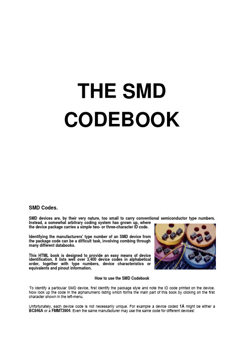
THE SMDCODEBOOKSMD Codes.SMD devices are, by their very nature, too small to carry conventional semiconductor type numbers. Instead, a somewhat arbitrary coding system has grown up, wherethe device package carries a simple two- or three-character ID code.Identifying the manufacturers' type number of an SMD device fromthe package code can be a difficult task, involving combing throughmany different databooks.This HTML book is designed to provide an easy means of deviceidentification. It lists well over 3,400 device codes in alphabeticalorder, together with type numbers, device characteristics orequivalents and pinout information.How to use the SMD CodebookTo identify a particular SMD device, first identify the package style and note the ID code printed on the device. Now look up the code in the alphanumeric listing which forms the main part of this book by clicking on the first character shown in the left-menu.Unfortunately, each device code is not necessarily unique. For example a device coded 1A might be either a BC846A or a FMMT3904. Even the same manufacturer may use the same code for different devices!If there is more than one entry, use the package style to differentiate between devices with the same ID code. This compilation has been collected from R P Blackwell G4PMK, manufacturers' data and other sources of SMD device ID codes, pinout and leaded device equivalent information.The entries under the Manufacturer column are not intended to be comprehensive; rather they are intended to provide help on locating sources of more detailed information if you require it.ID Code VariationsMany manufacturers use an extra letter as their own identification code. If the device is from Philips it will sometimes have a lower case 'p' (or sometimes 't') added to the code; Siemens devices usually have a lower case 's'.For example, if the code is 1A, according to the table there are a number of possibilities:• 1A BC846A Phi ITT N BC546A• 1A FMMT3904 Zet N 2N3904• 1A MMBT3904 Mot N 2N3904• 1A IRLML2402 IR F n-ch mosfet 20V 0.9AThis has been a problem in the past, however recently manufacturers have been adding lower case letters which clarify the code.Many recent Motorola devices have a small superscript letter after the device code, such as SA C . (This smaller letter is merely a month of manufacture code.)Many devices from Rohm Semiconductors which start with G have direct equivalents found in the rest of the number. For example GD1 is the same as D1 which is a BCW31.Some devices have a single coloured letter (usually on extremely small diode packages). Colour, if significant, is shown in small type after the code letter.An 'L' suffix usually indicates a low-profile package, such as an SOT323 orSC70.SOT323.SC70.Reverse joggle devices do present a few problems. They oftern have an 'R' in the type number. A reverse package is one where the lead have been bent up instead of down. So it's a mirror image of a conventional device. Identification is usually possible from the code number, but some manufacturers use the same code. In these cases, it's a case of looking at the device with a magnifying glass. The leads of most normal packages come out closer to the circuit board side of the device; conversely a reverse joggle package will have them coming out closer to the 'top' of the device.Sometimes a series of devices, derived from the same die, have related type (not code) numbers. Often an 'R' will indicate a reverse joggle package, and/or a 'W' indicate a smaller package variant, such as SOT343. Sometimes similarities are also found in the code numbers. For example:Recently some manufacturers have used a symbol or lower case letter to indicate the country of manufacture. These have been ignored in the alphabetical ordering. For example:• '67' is the code for a BFP67 (SOT143 package) ,• '67R' is the code for the reverse joggle variant BFP67R (SOT143R),• 'W67' is the code for a SOT343 package version.SOT143.'Z-S' and 'ZtS ' are both 2PC4081Q devices made by Philips; the first made in Hong Kong and the second in Malaysia; this appears in the codebook classified under ZS.Leaded equivalent device and informationWhere possible, the listing gives the part number of a conventional wire-leaded device with equivalent characteristics. If the leaded device is well-known then no more information is given. If the device is less common, some additional information will sometimes be given. Where no exact leaded equivalent exists, a brief device description is given, which may be sufficient to allow substitution with another device.When describing device characteristics, some terms are implied from the type of device. For example, a voltage specified for a rectifier diode is usually the maximum PIV (peak inverse voltage) of the diode, but for a zener diode the operating (zener voltage) will be given.Normally, where a voltage, current or power is specified, these will be limiting values. For example, a device specified as NPN 20V 0.1A 1W is a NPN transistor with a Vce (max) of 20V, maximum collector current of 100mA and a maximum total power dissipation of 1W. Some of the transistors are types with integrated resistors; in the list, a base resistor means a resistor connected in series with the base. When two resistor values are given, the first is the series base resistor, and the second the resistor between base and emitter.Digital Transistors (dtr)These are transistors with built-in resistors.Some have one resistor between base and emitter, others in series with the base. Many others have both.To keep things simple, the series resistor is called R1 and the base emitter resistor is called R2. If both are present, then two values are given, R1 first. So 4k7 + 10k means that R1 (the base resistor) is 4k7 and R2 (the resistor between base and emitter) is 10k.ConclusionIdentifying the manufacturers' type number of an SMD device from the package code can be a difficult task, involving combing through many different databooks. This HTML book is designed to provide an easy means of device identification.Abbreviationsamp amplifieratten attenuatora anodeb basec cathodeca common anodecc common cathodecomp complementd draindg dual gatedtr digital transistor (see codebook introduction) enh enhancement (mode - FETs)fet field effect transistorfT transition frequencyGaAsfet Gallium Arsenide field effect transistorg gategnd groundgp general purposehfe small signal current gaini/p inputId drain currentIg gate currentIr reverse leakage current (diodes)jfet junction field effect transistorMAG maximum available gainmax maximummin minimummmic microwave minature integrated circuit modamp modular amplifier - an mmic amplifier mosfet metal oxide insulated gate fetn-ch n-channel fet (any type)npn npn bipolar transistoro/p outputp-ch p-channel fet (any type)pin pin diodepkg packagepnp pnp bipolar transistorprot protection, protected (as in mosfet gate) res resistors sourceser seriesSi siliconsubstr substratesw switch or switchingVce collector - emitter voltage (maximum) Vcc collector supply voltageManufacturer abbreviationsAgi Agilent (was HP)Fch FairchildHP Hewlett-Packard (Now Agilent)Inf Infineon (was Siemens)ITT ITT SemiconductorsMC Mini-CircuitsMot Motorola (now ON Semiconductors) Nat National SemiconductorNec NECNJRC New Japan Radio CoON ON Semiconductors (was Motorola) Phi PhilipsRoh RohmSGS SGS-ThompsonSie Siemens (now Infineon)Sil Siliconix (Vishay-Silliconix)Tem Temic SemiconductorsTfk Telefunken (Vishay-Telefunken)Tok Toko Inc.Zet ZetexCodes beginning with '0'Code Device Manufacturer Base Package Leaded Equivalent/Data0 2SC3603 Nec CX SOT173 Npn RF fT 7GHz005 SSTPAD5 Sil J - PAD-5 5pA leakage diodep01 PDTA143ET Phi N SOT23 pnp dtr 4k7+4k7t01 PDTA143ET Phi N SOT23 pnp dtr 4k7+4k701 Gali-1 MC AZ SOT89 DC-8GHz MMIC amp 12dB gain 010 SSTPAD10 Sil J - PAD-10 10pA leakage diode 011 SO2369R SGS R SOT23R 2N236902 BST82 Phi M - n-ch mosfet 80V 175mA02 MRF5711L Mot X SOT143 npn RF MRF57102 DTCC114T Roh N - 50V 100mA npn sw + 10k base res 02 Gali-2 MC AZ SOT89 DC-8GHz MMIC amp 16dB gain p02 PDTC143ET Phi N SOT23 npn 4k7+4k7 bias rest02 PDTC143ET Phi N SOT23 npn 4k7+4k7 bias res03 Gali-3 MC AZ SOT89 DC-3GHz MMIC amp 22dB gain 03 DTC143TE Roh N EMT3 npn dtr R1 4k7 50V 100mA03 DTC143TUA Roh N SC70 npn dtr R1 4k7 50V 100mA03 DTC143TKA Roh N SC59 npn dtr R1 4k7 50V 100mA04 DTC114TCA Roh N SOT23 npn dtr R1 10k 50V 100mA 04 DTC114TE Roh N EMT3 npn dtr R1 10k 50V 100mA 04 DTC114TUA Roh N SC70 npn dtr R1 10k 50V 100mA 04 DTC114TKA Roh N SC59 npn dtr R1 10k 50V 100mA 04 MRF5211L Mot X SOT143 pnp RF MRF52104 Gali-4 MC AZ SOT89 DC-4GHz MMIC amp 17.5 dBm -04 PMSS3904 Phi N SOT323 2N3904t04 PMBS3904 Phi N SOT23 2N390405 Gali-4 MC AZ SOT89 DC-4GHz MMIC amp 18 dBm o/p 05 DTC124TE Roh N EMT3 npn dtr R1 22k 50V 100mA 05 DTC124TUA Roh N SC70 npn dtr R1 22k 50V 100mA 05 DTC124TKA Roh N SC59 npn dtr R1 22k 50V 100mA 05F TSDF1205R Tfk WQ - fT12GHz npn 4V 5mA06 Gali-6 MC AZ SOT89 DC-4GHz MMIC amp 115 dBm o/p 06 DTC144TE Roh N EMT3 npn dtr R1 47k 50V 100mA 06 DTC144TUA Roh N SC70 npn dtr R1 47k 50V 100mA 06 DTC144TKA Roh N SC59 npn dtr R1 47k 50V 100mA-06 PMSS3906 Phi N SOT323 2N3906t06 PMBS3906 Phi N SOT23 2N3906020 SSTPAD20 Sil J - PAD-20 20pA leakage diode 050 SSTPAD50 Sil J - PAD-50 50pA leakage diode 081 SO2369AR SGS R SOT23R 2N2369A09 DTC115TUA Roh N SC70 npn dtr R2 100k 50V 100mA 09 DTC115TKA Roh N SC59 npn dtr R2 100k 50V 100mA0A MUN5111DW1 Mot DO SOT363 dual pnp dtr 10k+10k0A DTC125TUA Roh N SC70 npn dtr R2 100k 50V 100mA0A DTC125TKA Roh N SC59 npn dtr R2 100k 50V 100mA0B MUN5112DW1 Mot DO SOT363 dual pnp dtr 22k+22k0C MUN5113DW1 Mot DO SOT363 dual pnp dtr 47k+47k0D MUN5114DW1 Mot DO SOT363 dual pnp dtr 10k+47k0E MUN5115DW1 Mot DO SOT363 dual pnp dtr R1 10k0F MUN5116DW1 Mot DO SOT363 dual pnp dtr R1 4k70G MUN5130DW1 Mot DO SOT363 dual pnp dtr 1k0+1k00H MUN5131DW1 Mot DO SOT363 dual pnp dtr 2k2+2k20J MUN5132DW1 Mot DO SOT363 dual pnp dtr 4k7+4k70K MUN5133DW1 Mot DO SOT363 dual pnp dtr 4k7+47k0L MUN5134DW1 Mot DO SOT363 dual pnp dtr 22k+47k0M MUN5135DW1 Mot DO SOT363 dual pnp dtr 2k2+47kCodes beginning with '1'Code Device Manufacturer Base Package Leaded Equivalent/Data1 2SC3587 Nec CX - npn RF fT10GHz1 BA277 Phi I SOD523 VHF Tuner band switch diode1 (red) BB669 Sie I SOD323 56-2.7 pF varicap10 MRF9411L Mot X SOT143 npn Rf 8GHz MRF94110A PZM10NB2A Phi A SOT346 dual ca 10V 0.3W zener10V PZM10NB Phi C SOT346 10V 0.3W zener10Y BZV49-C10 Phi O SOT89 10V 1W zener11 MRF9511L Mot X SOT143 npn RF 8GHz MRF95111 MUN5311DW1 Mot DP SOT363 npn/pnp dtr 10k+10k11 PDTA114EU Phi N SOT416 pnp dtrp11 PDTA114TT Phi N SOT23 pnp dtrt11 PDTA114TT Phi N SOT23 pnp dtr11A PZM11NB2A Phi A SOT346 dual ca 11V 0.3W zener11A MMBD1501A Nat C SOT23 Si diode 200V 100mA11V PZM11NB Phi C SOT346 11V 0.3W zener11Y BZV49-C11 Phi O SOT89 11V 1W zener12 MUN5312DW1 Mot DP SOT363 npn/pnp dtr 22k+22k12 DTA123EUA Rho N SC70 pnp dtr 2k2+2k2 50V 100ma12 DTA123EKA Rho N SC59 pnp dtr 2k2+2k2 res 50V 100ma p12 PDTC114TT Phi N SOT23 npn dtrt12 PDTC114TT Phi N SOT23 npn dtr12A MMBD1502A Nat K SOT23 Si diode 200V 100mA12A PZM12NB2A Phi A SOT346 dual ca 12V 0.3W zener12E ZC2812E Zet D SOT23 dual series RF schottky15V 20mA 12V PZM12NB Phi C SOT346 12V 0.3W zener12Y BZV49-C12 Phi O SOT89 12V 1W zener13 DTA143EUA Rho N SC70 pnp dtr 4k7+4k7 50V 100ma13 DTA143EKA Rho N SC59 pnp dtr 4k7+4k7 50V 100ma13 DTA143ECA Rho N SOT23 pnp dtr 4k7+4k7 50V 100ma13t BC846BPN Phi N SOT363 BC546B13s BAS125 Sie C SOT23 Schottky sw 24V 100mA13s BAS125W Sie C SOT323 Schottky sw 24V 100mA13 MA4CS103A M/A C SOT23 Schottky RF 20V 100mA13 MUN5313DW1 Mot DP SOT363 npn/pnp dtr 47k+47k13A MMBD1503A Nat D SOT23 dual Si diode 200V 100mA 13A PZM13NB2A Phi A SOT346 dual ca 13V 0.3W zener13E ZC2813E Zet A SOT23 dual ca RF schottky15V 20mA 13V PZM13NB Phi C SOT346 13V 0.3W zener13Y BZV49-C13 Phi O SOT89 13V 1W zener14s BAS125-04 Sie D SOT23 Dual series Schottky 25V 100mA 14s BAS125-04W Sie D SOT323 Dual series Schottky 25V 100mA 14 BAT114-099R Sie DQ - Quad Schottky crossover ring 14 DTA114EUA Roh N SC70 pnp dtr 10k + 10k14 DTA114EKA Roh N SC59 pnp dtr 10k + 10k14 MUN5314DW1 Mot DP SOT363 npn/pnp dtr 10k R114 DTA114ECA Roh N SOT23 pnp dtr 10k + 10k14A MMBD1504A Nat B - dual cc Si diode 200V 100mA 15s BAS125-05 Sie B SOT23 dual cc Schottky 25V 100mA 15s BAS125-05W Sie B SOT323 dual cc Schottky 25V 100mA 15 DTA124EUA Roh N SC70 pnp dtr 30V 50mA 22k+22k 15 DTA124EKA Roh N SC59 pnp dtr 30V 50mA 22k+22k 15 DTA124ECA Roh N SOT23 pnp dtr 30V 50mA 22k+22k 15 MUN5315DW1 Mot DP SOT363 npn/pnp dtr 10k R115 MMBT3960 Mot N - 2N396015A MMBD1505A Nat A - dual ca Si diode 200V 100mA 15A PZM15NB2A Phi A SOT346 dual ca 15V 0.3W zener15V PZM15NB Phi C SOT346 15V 0.3W zener15Y BZV49-C15 Phi O SOT89 15V 1W zenerp16 PDTC114ET Phi N SOT23 npn dtrt16 PDTC114EU Phi N SOT323 npn dtr16s BAS125-06 Sie A SOT23 dual ca Schottky 25V 100mA 16s BAS125-06W Sie A SOT323 dual ca Schottky 25V 100mA 16 MUN5316DW1 Mot DP SOT363 npn/pnp dtr 4k7 R116 DTA144EUA Roh N SC70 pnp dtr 30V 50mA 47k+47k 16 DTA144EKA Roh N SC59 pnp dtr 30V 50mA 47k+47k 16V PZM16NB Phi C SOT346 16V 0.3W zener16Y BZV49-C16 Phi O SOT89 16V 1W zener17s BAS125-07 Sie S SOT143 dual Schottky 25V 100mA 17s BAS125-07W Sie S SOT343 dual Schottky 25V 100mAp17 PDTC124ET Phi N SOT23 npn dtrt17 PDTC124EU Phi N SOT323 npn dtr18 BFP181T Tfk X - npn Rf fT 7.8GHz 10V 20mA 18 PDTC143ZK Phi N SOT346 npn dtr 4k7+47kp18 PDTC143ZT Phi N SOT23 npn dtr 4k7+47kt18 PDTC143ZT Phi N SOT23 npn dtr 4k7+47k18V PZM18NB Phi C SOT346 18V 0.3W zener18Y BZV49-C18 Phi O SOT89 18V 1W zener19 PDTA143ZK Phi N SOT346 pnp dtr 4k7+47k19 DTA115EUA Rho N SC70 pnp dtr 100k+100k 50V 100ma 19 DTA115EKA Rho N SC59 pnp dtr 100k+100k 50V 100ma p19 PDTA143ZT Phi N SOT23 pnp dtr 4k7+47kt19 PDTA143ZT Phi N SOT23 pnp dtr 4k7+47k100 SSTPAD100 Sil J SOT23 PAD-100 100pA leakage diode 101 PZM10NB1 Phi C SOT346 10V 0.3W zener102 PZM10NB2 Phi C SOT346 10V 0.3W zener103 PZM10NB3 Phi C SOT346 10V 0.3W zener111 PZM11NB1 Phi C SOT346 11V 0.3W zener111 DTA113ZUA Roh N SC70 pnp dtr 1k+10k 50V 100mA 112 PZM11NB2 Phi C SOT346 11V 0.3W zener113 PZM11NB3 Phi C SOT346 11V 0.3W zener113 DTA143ZUA Roh N SC70 pnp dtr 4k7+47k 50V 100mA 121 PZM12NB1 Phi C SOT346 12V 0.3W zener121 DTC113ZUA Roh N SC70 npn dtr 1k+10k 50V 100mA 122 PZM12NB2 Phi C SOT346 12V 0.3W zener123 PZM12NB3 Phi C SOT346 12V 0.3W zener123 DTC143ZUA Roh N SC70 npn dtr 4k7+47k 50V 100mA 131 PZM13NB1 Phi C SOT346 13V 0.3W zener132 PZM13NB2 Phi C SOT346 13V 0.3W zener132 DTA123JUA Roh N SC70 pnp dtr 2k2+47k 50V 100mA 133 PZM13NB3 Phi C SOT346 13V 0.3W zener142 DTA123JUA Roh N SC70 npn dtr 2k2+47k 50V 100mA 151 PZM15NB1 Phi C SOT346 15V 0.3W zener152 PZM15NB2 Phi C SOT346 15V 0.3W zener153 PZM15NB3 Phi C SOT346 15V 0.3W zener156 DTA144VUA Roh N SC70 pnp dtr 47k+10k 50V 100mA 161 PZM16NB1 Phi C SOT346 16V 0.3W zener162 PZM16NB2 Phi C SOT346 16V 0.3W zener163 PZM16NB3 Phi C SOT346 16V 0.3W zener166 DTC144VUA Roh N SC70 npn dtr 47k+10k 50V 100mA 179 FMMT5179 Zet N - 2N5179181 PZM18NB1 Phi C SOT346 18V 0.3W zener182 PZM18NB2 Phi C SOT346 18V 0.3W zener183 PZM18NB3 Phi C SOT346 18V 0.3W zener1A BC846A Phi N SOT23 BC546A1A BC846AT Phi N SOT416 BC546A1Ap BC846A Phi N SOT23 BC546A1At BC846A Phi N SOT23 BC546A1At BC846AW Phi N SOT323 BC546A1A- BC846AW Phi N SOT323 BC546A1A FMMT3904 Zet N SOT23 2N39041A MMBT3904 Mot N SOT23 2N39041A IRLML2402 IR F SOT23 n-ch mosfet 20V 0.9Ap1A PMMT3904 Phi N SOT23 2N3904p1A PXT3904 Phi N SOT89 2N3904t1A PMMT3904 Phi N SOT23 2N3904t1A PMST3904 Phi N SOT323 2N3904-1A PMST3904 Phi N SOT323 2N39041AM MMBT3904L Mot N SOT23 2N39041B BC846B Phi N SOT23 BC546B1B BC846BT Phi N SOT416 BC546B1Bp BC846B Phi N SOT23 BC546B1Bt BC846B Phi N SOT23 BC546B1Bt BC846BW Phi N SOT323 BC546B1B- BC846BW Phi N SOT323 BC546B1B FMMT2222 Zet N SOT23 2N22221B MMBT2222 Mot N SOT23 2N22221B IRLML2803 IR F SOT23 n-ch mosfet 30V 0.9Ap1B PMBT2222 Phi N SOT23 2N2222t1B PMBT2222 Phi N SOT23 2N2222t1B PMST2222 Phi N SOT233 2N2222-1B PMST2222 Phi N SOT323 2N22221Bs BC817UPN Sie N SC74 -1Cp BAP50-05 Phi B SOT23 dual cc GP RF pin diode 1C FMMT-A20 Zet N SOT23 MPSA201C MMBTA20L Mot N SOT23 MPS39041C IRLML6302 IR F SOT23 p-ch mosfet 20V 0.6A1Cs BC847S Sie - SOT363 BC4571Dp BC846 Phi N SOT23 BC4561Dt BC846 Phi N SOT23 BC4561Dt BC846W Phi N SOT323 BC4561D- BC846W Phi N SOT323 BC4561D MMBTA42 Mot N SOT23 MPSA42 300V npn1D IRLML5103 IR F SOT23 p-ch mosfet 30V 0.6Ap1D PMBTA42 Phi N SOT23 MPSA42 300V npnp1D PXTA42 Phi N SOT89 MPSA42 300V npnt1D PMBTA42 Phi N SOT23 MPSA42 300V npnt1D PMSTA42 Phi N SOT323 MPSA42 300V npn1Ds BC846U Sie N SC74 BC4561Ds BC846U Sie - SOT363 BC4561DN 2SC4083 Roh N - npn 11V 3.2GHz TV tuners 1DR MSD1328R Mot N SOT346 npn gp 25V 500mA1E BC847A Phi N SOT23 BC547A1E BC847AT Phi N SOT416 BC547A1Ep BC847A Phi N SOT23 BC547A1Et BC847A Phi N SOT23 BC547A1Et BC847A Phi N SOT323 BC547A1E- BC847A Phi N SOT323 BC547A1ER BC847AR Phi R SOT23R BC547A1E FMMT-A43 Zet N - MPSA431E MMBTA43 Mot N SOT23 MPSA43 200V npnt1E PMBTA43 Mot N SOT23 MPSA43 200V npnt1E PMSTA43 Mot N SOT323 MPSA43 200V npn1Es BC847A Sie N SOT23 BC4571Es BC847AW Sie N SOT323 BC4571EN 2SC4084 Roh N - npn 20V 2.0GHz TV tuners 1F BC847B Phi N SOT23 BC547B1F BC847BT Phi N SOT416 BC547B1Fs BC847B Sie N SOT23 BC547B1Fs BC847BT Sie N SC75 BC547B1Fs BC847BW Sie N SOT323 BC547B1Fp BC847B Phi N SOT23 BC547B1Ft BC847B Phi N SOT23 BC547B1Ft BC847BW Phi N SOT323 BC547B1F- BC847BW Phi N SOT323 BC547B1FR BC847BR Phi R SOT23R BC547B1F MMBT5550 Mot N SOT23 2N5550 140V npnp1F PMBT5550 Phi N SOT23 2N5550 140V npnt1F PMBT5550 Phi N SOT23 2N5550 140V npnt1F PMST5550 Phi N SOT323 2N5550 140V npn1FZ FMBT5550 Zet N SOT23 2N5550 140V npn1G BC847C Phi N SOT23 BC547C1G BC847CT Phi N SOT416 BC547C1Gp BC847C Phi N SOT23 BC547C1Gt BC847CW Phi N SOT323 BC547C1G- BC847CW Phi N SOT323 BC547C1Gs BC847C Sie N SOT23 BC547C1Gs BC847CW Sie N SOT323 BC547C1GR BC847CR Phi R SOT23R BC547C1GT SOA06 SGS N SOT23 MPSA061G FMMT-A06 Zet N SOT23 MPSA061G MMBTA06 Mot N SOT23 MPSA06p1G PMMTA06 Phi N SOT23 MPSA06t1G PMMTA06 Phi N SOT23 MPSA06t1G PMMTA06 Phi N SOT323 MPSA061GM MMBTA06 Mot N SOT23 MPSA061Hp BC847 Phi N SOT23 BC5471Ht BC847 Phi N SOT23 BC5471Ht BC847W Phi N SOT323 BC5471H- BC847W Phi N SOT323 BC5471H FMMT-A05 Zet N - MPSA051H MMBTA05 Mot N SOT23 MPSA05t1H MMBTA05 Phi N SOT323 MPSA051HT SOA05 SGS N SOT23 MPSA051J BC848A Phi N SOT23 BC548A1Js BC848A Sie N SOT23 BC548A1Js BC848AW Sie N SOT323 BC548A1J FMMT2369 Zet N SOT23 2N23691J MMBT2369 Mot N SOT23 MPS23691Js BCV61A Sie VQ SOT143 npn current mirror hFe 180 1Jp BCV61A Phi VQ SOT143 npn current mirror hFe 180 p1J PMBT2369 Phi N SOT23 2N2369t1J PMBT2369 Phi N SOT23 2N2369t1J PMBT2369 Phi N SOT323 2N23691JA MMBT2369A Mot N SOT23 MPS2369A1JR BC848AR Phi R SOT23R BC548A1JZ BC848A Zet N SOT23 BC548A1K BC848B ITT N SOT23 BC548B1Kp BC848B Phi N SOT23 BC548B1Ks BC848B Sie N SOT23 BC548B1Ks BC848BW Sie N SOT323 BC548B1K MMBT6428 Mot N SOT23 MPSA18 50Vp1K PMBT6428 Phi N SOT23 MPSA18 50Vt1K PMBT6428 Phi N SOT23 MPSA18 50Vt1K PMBT6428 Phi N SOT323 MPSA18 50V1K FMMT4400 Zet N SOT23 2N44001Ks BCV61B Sie VQ SOT143B npn current mirror hFe 290 1Kp BCV61B Phi VQ SOT143B npn current mirror hFe 290 1KR BC848BR Phi R SOT23R BC548B1KM MMBT6428L Mot N SOT23 MPSA18 50V1KZ FMMT4400 Zet N SOT23 2N44001L BC848C ITT N SOT23 BC548C1Lp BC848C Phi N SOT23 BC548C1Ls BC848C Sie N SOT23 BC548C1Ls BC848CW Sie N SOT323 BC548C1L MMBT6429 Mot N - MPSA18 45V1L FMMT4401 Zet N - 2N44011L BCV61C Sie VQ SOT143B npn current mirror hFe 520 1Lp BCV61C Phi VQ SOT143B npn current mirror hFe 520 p1L PMBT6429 Phi N SOT23 MPSA18 45Vt1L PMBT6429 Phi N SOT23 MPSA18 45Vt1L PMBT6429 Phi N SOT323 MPSA18 45V1LR BC848CR Phi R SOT23R BC548C1Mp BC848 Phi N SOT23 BC5481M MMBTA13 Mot N SOT23 MPSA13 darlington1Mp BCV61 Phi VQ SOT143B npn current mirror1M FMMT-A13 Zet N SOT23 MPSA13p1M PXTA13 Phi N SOT89 MPSA13 darlingtonp1M PMBTA13 Phi N SOT23 MPSA13 darlingtont1M PMBTA13 Phi N SOT23 MPSA13 darlington1N FMMT-A14 Zet N SOT23 MPSA141N MMBTA14 Mot N SOT23 MPSA14 darlington1N5 ZTX11N15DF Zet N SOT23 npn 15V 3A low saturation V p1N PMBTA14 Mot N SOT23 MPSA14 darlingtonp1N PXTA14 Mot N SOT89 MPSA14 darlingtont1N PMBTA14 Mot N SOT23 MPSA14 darlington1P FMMT2222A Zet N - 2N2222A1P MMBT2222A Mot N SOT23 2N2222A1P BC847PN Sie DI - pnp/npn separate pair gp AF p1P PMBT2222A Phi N SOT23 2N2222Ap1P PXT2222A Phi N SOT89 2N2222At1P PMBT2222A Phi N SOT23 2N2222At1P PMST2222A Phi N SOT323 2N2222A1Q MMBT5088 Mot N SOT23 MPSA18 Vce 30Vp1Q PMBT5088 Phi N SOT23 MPSA18 Vce 30Vt1Q PMBT5088 Phi N SOT23 MPSA18 Vce 30Vt1Q PMST5088 Phi N SOT323 MPSA18 Vce 30V1R MMBT5089 Mot N SOT23 MPSA18 Vce 25Vt1R PMST5089 Phi N SOT323 MPSA18 Vce 25V1S MMBT2369A Nat N SOT23 2N2369A 500MHz sw npn 1S MSC3130 Mot H SOT346 npn RF fT 1.4GHz 10V1T MMBT3960A Mot N - 2N3960A1U MMBT2484L Mot N SOT23 MPSA181V MMBT6427 Mot H SOT23 2N6426/7 darlington npn 1Vp BF820 Phi N SOT23 npn 300V 50mA BF4201Vt BF820 Phi N SOT23 npn 300V 50mA BF4201Vt BF820W Phi N SOT323 npn 300V 50mA BF4201V- BF820W Phi N SOT323 npn 300V 50mA BF4201W FMMT3903 Zet N SOT23 2N39031Wp BF821 Phi N SOT23 pnp 300V 50mA BF421 1Wt BF821 Phi N SOT23 pnp 300V 50mA BF4211W t BF822W Phi N SOT323 pnp 300V 50mA BF4211W - BF822W Phi N SOT323 pnp 300V 50mA BF421 1X MMBT930L Mot N SOT23 MPS39041Xp BF822 Phi N SOT23 npn 250V 50mA BF422 1Xt BF822 Phi N SOT23 npn 250V 50mA BF422 1Y MMBT3903 Mot N SOT23 2N39031Yp BF823 Phi N SOT23 pnp 250V 50mA BF423 1Yt BF823 Phi N SOT23 pnp 250V 50mA BF423 1Z BAS70-06 Zet A SOT23 dual RF CA schottky diode 1Z MMBT6517 Mot N SOT23 2N6517 npn Vce 350VCodes beginning with '2'Code Device Manufacturer Base Package Leaded Equivalent/Data2 BAT62-02W Sie I SCD80 BAT16 schottky diode2 (blue) BAR64-03W Sie I SOD323 pin diode2 2SC3604 Nec CX - npn RF fT8GHz 12dB@2GHz 2 (white) BB439 Sie I SOD323 29-5 pF varicap20 MRF5811 Mot X SOT143 npn Rf fT 5GHz 0.2A-20 PDTC114WU Phi N SOT323 npn dtr20F TSDF1220 Tfk X SOT143 fT 12GHz npn 6V 20mA 20V PZM20NB Phi C SOT346 20V 300mW zener 20Y BZV49-C20 Phi O SOT89 20V 1W zener21 Gali-21 MC AZ SOT89 DC-8GHz MMIC amp 14 dB gain22 MMBT4209 Nat N SOT23 pnp sw 850MHz 2N420922 DTC123EUA Rho N SC70 npn dtr 2k2+2k2 50V 100ma22 DTC123EKA Rho N SC59 npn dtr 2k2+2k2 50V 100ma22V PZM22NB Phi C SOT346 22V 300mW zener 22Y BZV49-C22 Phi O SOT89 22V 1W zener23 MMBT3646 Nat N SOT23 npn sw 350MHz 2N364623 DTC143EUA Roh N SC70 pnp dtr 50V 100mA 4k7+ 4k723 DTC143EKA Roh N SC59 pnp dtr 50V 100mA 4k7+ 4k7-23 PDTA114TU Phi N SOT323 pnp dtr R1 10k t23 PDTA114TU Phi N SOT323 pnp dtr R1 10k24 MMBD2101 Nat C SOT23 Si diode 100V 200mA24 DTC114ECA Roh N SOT23 npn dtr 50V 100mA 10k + 10k24 DTC114EUA Roh N SC70 npn dtr 50V 100mA 10k + 10k24 DTC114EKA Roh N SC59 npn dtr 50V 100mA 10k + 10k24 2SC5006 Nec N - npn RF fT 4.5GHz @3V 7mA-24 PDTC114TU Phi N SOT323 npn dtr R1 10k t24 PDTC114TU Phi N SOT323 npn dtr R1 10k 24V PZM24NB Phi C SOT346 24V 300mW Zener 24Y BZV49-C24 Phi O SOT89 24V 1W zener25 MMBD2102 Nat K SOT23 Si diode 100V 200mA25 DTC124ECA Roh N SOT23 npn dtr 50V 100mA 22k + 22k25 DTC124EKA Roh N SC59 npn dtr 50V 100mA 22k + 22k25 DTC124EUA Roh N SC70 npn dtr 50V 100mA 22k + 22k26 MMBD2103 Nat D SOT23 dual MMBD120126 DTC144EKA Roh N SC59 npn dtr 50V 30mA 47k + 47k26 DTC144EUA Roh N SC70 npn dtr 50V 30mA 47k + 47k27 MMBD2104 Nat B SOT23 dual cc MMBD120127V PZM27NB Phi C SOT346 27V 300mW Zener 27Y BZV49-C27 Phi O SOT89 27V 1W zener28 BFP280T Tfk W - npn RF fT 7GHz 8V 10mA28 MMBD2105 Nat A SOT23 dual ca MMBD1201-28 PDTA114WU Phi N SOT323 pnp dtr29 MMBD1401 Nat C SOT23 Si diode 200V 100mA29 DTC115EE Roh N EMT3 npn dtr 100k +100k 50V 20mA29 DTC115EUA Roh N SC70 npn dtr 100k +100k 50V 20mA29 DTC115EKA Roh N SC59 npn dtr 100k +100k 50V 20mA200 SSTPAD200 Sil J - PAD-200 200pA leakage diode 201 PZM20NB1 Phi C SOT346 20V 300mW Zener202 PZM20NB2 Phi C SOT346 20V 300mW Zener 203 PZM20NB3 Phi C SOT346 20V 300mW Zener 221 PZM22NB1 Phi C SOT346 22V 300mW Zener 222 PZM22NB2 Phi C SOT346 22V 300mW Zener 223 PZM22NB3 Phi C SOT346 22V 300mW Zener 241 PZM24NB Phi C SOT346 24V 300mW Zener 242 PZM24NB Phi C SOT346 24V 300mW Zener 243 PZM20NB Phi C SOT346 24V 300mW Zener 271 PZM2.7NB1 Phi C SOT346 2.7V 300mW Zener 272 PZM2.7NB2 Phi C SOT346 2.7V 300mW Zener 2A MMBT3906L Mot N SOT23 2N39062A MMBT3906W Mot N SOT323 2N39062A FMMT3906 Zet N SOT23 2N3906t2A PMBT3906 Phi N SOT23 2N3906t2A PMST3906 Phi N SOT323 2N3906p2A PMBT3906 Phi N SOT23 2N3906p2A PXT3906 Phi O SOT89 2N39062A4 PZM2.4NB2A Phi A SOT346 dual 2.4V cc Zener2A7 PZM2.7NB2A Phi A SOT346 dual 2.7V cc Zener2B BC849B ITT N SOT23 BC549B2Bs BC849B Sie N SOT23 BC549B2Bs BC849BW Sie N SOT323 BC549B2Bp BC849B Phi N SOT23 BC549B2Bt BC849BW Phi N SOT323 BC549B2B- BC849BW Phi N SOT323 BC549B2B FMMT2907 Zet N SOT23 2N29072B MMBT2907 Mot N SOT23 MPS2907p2B PMBT2907 Phi N SOT23 2N2907t2B PMBT2907 Phi N SOT23 2N29072BR BC849BR Phi R SOT23R BC549B2BZ FMMT2907 Zet N SOT23 2N29072C BC849C ITT N SOT23 BC549C2Cs BC849C Sie N SOT23 BC549C2Cs BC849CW Sie N SOT323 BC549C2Cp BC849C Phi N SOT23 BC549C2Ct BC849C Phi N SOT23 BC549C2Ct BC849CW Phi N SOT323 BC549C2C- BC849CW Phi N SOT323 BC549C2C MMBTA70 Mot N SOT23 MPSA702CR BC849CR Phi R SOT23R BC549C2CZ FMMTA70 Zet N SOT23 MPSA702D MMBTA92 Mot N SOT23 MPSA92 pnp Vce 300V p2D PMBTA92 Phi N SOT23 MPSA92 pnp Vce 300V p2D PXTA92 Phi O SOT89 MPSA92 pnp Vce 300V t2D PMBTA92 Phi N SOT23 MPSA92 pnp Vce 300V t2D PMSTA92 Phi N SOT323 MPSA92 pnp Vce 300V 2E MMBTA93 Mot N SOT23 MPSA93 pnp Vce 200V 2E FMMT-A93 Zet N SOT23 MPSA93t2E PMBTA93 Phi N SOT23 MPSA93 pnp Vce 200V t2E PMSTA93 Phi N SOT323 MPSA93 pnp Vce 200V 2F BC850B ITT N SOT23 BC550B2Fs BC850B Sie N SOT23 BC550B2Fs BC850BW Sie N SOT323 BC550B2Fp BC850B Phi N SOT23 BC550B2Ft BC850B Phi N SOT23 BC550B2Ft BC850BW Phi N SOT323 BC550B2F- BC850BW Phi N SOT323 BC550B2F FMMT2907A Zet N SOT23 2N2907A2F MMBT2907A Mot N SOT23 MPS2907A2F MMBT2907AW Mot N SOT323 MPS2907Ap2F PMBT2907A Phi N SOT23 2N2907Ap2F PXT2907A Phi O SOT89 2N2907At2F PMBT2907A Phi N SOT23 2N2907At2F PMBT2907A Phi N SOT323 2N2907A2FR BC850BR Phi R SOT23R BC550B。
- 1、下载文档前请自行甄别文档内容的完整性,平台不提供额外的编辑、内容补充、找答案等附加服务。
- 2、"仅部分预览"的文档,不可在线预览部分如存在完整性等问题,可反馈申请退款(可完整预览的文档不适用该条件!)。
- 3、如文档侵犯您的权益,请联系客服反馈,我们会尽快为您处理(人工客服工作时间:9:00-18:30)。
ELECTRICAL CHARACTERISTICS
(VDD = 2.7V to 3.6V (MAX1237/MAX1239), VDD = 4.5V to 5.5V (MAX1236/MAX1238), VREF = 2.048V (MAX1237/MAX1239), VREF = 4.096V (MAX1236/MAX1238), fSCL = 1.7MHz, TA = TMIN to TMAX, unless otherwise noted. Typical values are at TA = +25°C, see Tables 1–5 for programming notation.)
REF to GND ............-0.3V to the lower of (VDD + 0.3V) and 6V SDA, SCL to GND.....................................................-0.3V to +6V Maximum Current Into Any Pin .........................................±50mA Continuous Power Dissipation (TA = +70°C)
Selector Guide
PART
INPUT CHANNELS
INTERNAL REFERENCE
(V)
SUPPLY VOLTAGE
(V)
INL (LSB)
MAX1236
4
MAX1237
4
MAX1238
12
MAX1239
12
4.096 2.048 4.096 2.048
4.5 to 5.5 ±1 2.7 to 3.6 ±1 4.5 to 5.5 ±1 2.7 to 3.6 ±1
670µA at 94.4ksps 230µA at 40ksps 60µA at 10ksps 6µA at 1ksps 0.5µA in Power-Down Mode
♦ Software-Configurable Unipolar/Bipolar ♦ Small Packages
8-Pin µMAX (MAX1236/MAX1237) 16-Pin QSOP (MAX1238/MAX1239)
♦ Internal Reference 2.048V (MAX1237/MAX1239) 4.096V (MAX1236/MAX1238)
♦ External Reference: 1V to VDD ♦ Internal Clock ♦ 4-Channel Single-Ended or 2-Channel Fully
Differential (MAX1236/MAX1237)
♦ 12-Channel Single-Ended or 6-Channel Fully Differential (MAX1238/MAX1239)
♦ Internal FIFO with Channel-Scan Mode ♦ Low Power
For pricing, delivery, and ordering information, please contact Maxim Direct at 1-888-629-4642, or visit Maxim’s website at .
/
Pin Configurations and Typical Operating Circuit appear at end of data sheet.
________________________________________________________________ Maxim Integrated Products 1
The full-scale analog input range is determined by the internal reference or by an externally applied reference voltage ranging from 1V to VDD. The MAX1237/ MAX1239 feature a 2.048V internal reference and the MAX1236/MAX1238 feature a 4.096V internal reference. The MAX1236/MAX1237 are available in an 8-pin µMAX® package. The MAX1238/MAX1239 are available in a 16pin QSOP package. The MAX1236–MAX1239 are guaranteed over the extended temperature range (-40°C to +85°C). For pin-compatible 10-bit parts, refer to the MAX1136–MAX1139 data sheet. For pin-compatible 8-bit parts, refer to the MAX1036–MAX1039 data sheet.
Features
♦ High-Speed I2C-Compatible Serial Interface 400kHz Fast Mode 1.7MHz High-Speed Mode
♦ Single-Supply 2.7V to 3.6V (MAX1237/MAX1239) 4.5V to 5.5V (MAX1236/MAX1238)
0110101 0110101
MAX1239EEE+ -40°C to +85°C 16 QSOP 0110101
+Denotes a lead(Pb)-free/RoHS-compliant package. /V denotes an automotive qualified part.
AutoShutdown is a trademark of Maxim Integrated Products, Inc. µMAX is a registered trademark of Maxim Integrated Products, Inc.
19-2333; Rev 7; 5/10
MAX1236–MAX1239
2.7V to 3.6V and 4.5V to 5.5V, Low-Power, 4-/12-Channel, 2-Wire Serial, 12-Bit ADCs
General Description
The MAX1236–MAX1239 low-power, 12-bit, multichannel analog-to-digital converters (ADCs) feature internal track/hold (T/H), voltage reference, clock, and an I2C-compatible 2-wire serial interface. These devices operate from a single supply of 2.7V to 3.6V (MAX1237/ MAX1239) or 4.5V to 5.5V (MAX1236/MAX1238) and require only 670µA at the maximum sampling rate of 94.4ksps. Supply current falls below 230µA for sampling rates under 46ksps. AutoShutdown™ powers down the devices between conversions, reducing supply current to less than 1µA at low throughput rates. The MAX1236/MAX1237 have four analog input channels each, while the MAX1238/MAX1239 have 12 analog input channels each. The fully differential analog inputs are software configurable for unipolar or bipolar, and single-ended or differential operation.
Applications
Handheld Portable Applications Medical Instruments Battery-Powered Test Equipment
Solar-Powered Remote Systems Received-Signal-Strength Indicatnd those listed under “Absolute Maximum Ratings” may cause permanent damage to the device. These are stress ratings only, and functional operation of the device at these or any other conditions beyond those indicated in the operational sections of the specifications is not implied. Exposure to absolute maximum rating conditions for extended periods may affect device reliability.
Ordering Information
PART