TC2000中文资料
CTX gamma2000TC几何精度--中文版

1 / 4精度检验表CTX gamma 2000TC序号 测量目标 视图 测试 说明偏离值允许值 实测值 1机床校准: A 、 纵向方向; B 、 交叉方向水平校准放置水平仪于Y 轴滑枕上部,通过移动床身来测量水平。
0.02mm/mA 、B 、2机床主轴跳动: A 、 轴向 B 、 径向使用千分表,依据DIN879测量标准A 、 千分表测量主轴平端面;B 、 千分表测量主轴外圆面。
转动主轴看千分表读数。
0.01mm主轴: A 、 B 、 副主轴: A 、 B 、3机床刀具主轴端面跳动使用千分表,依据DIN879测量标准千分表测量刀具主轴平端面,转动刀具主轴,查看千分表读数。
0.003mm4机床刀具主轴跳动使用千分表,依据DIN879测量标准把校棒插入机床刀具主轴,转动主轴,使用秒表分别测量a、b两点,得出读数。
A、0.005mmB、0.015mmA、B、5 测量车削主轴和刀具主轴平行度:A、X方向B、Y方向使用千分表和校棒,依据DIN879测量标准校棒插入车削主轴,使用千分表从c点水平移动至d点,读千分表读数。
主轴A、0.005mmB、0.008mmX方向A、B、副主轴A、0.005mmB、0.008mmY方向A、B、6 刀具主轴和车削主轴的同轴度:A、X方向B、Y方向使用千分表、测量臂和校棒,依据DIN879测量标准放置测量表座在刀具主轴S1上,安装校棒于车削主轴上,放置千分表针于c点,转动车削主轴180°,取千分表0度和180度差值读数,将该数值除以2及为误差值调整千分表至d点位置,重复测量。
在第二个平面上重复测量。
主轴A、0.010mmB、0.015mmA、B、副主轴A、0.030mmB、0.030mmA、B、7 测量刀具主轴之平行度:A、Z/X方向使用千分表和校棒,依据DIN879测插入校棒至刀具主轴,B轴转至0°位置,千分表针头放于c点位置,移动千分表至dA、0.01mmB、0.02mm0°A、B、2 / 43 / 4B、 Y 方向量标准点,读千分表之读数。
德国 TC2000S经颅多普勒检修1例
德国 TC2000S经颅多普勒检修1例
马伟民;孙文乔
【期刊名称】《中国医疗设备》
【年(卷),期】2002(017)002
【摘要】@@ 故障现象机器时而不能启动,时而启动后却发现无显示,进入死机状态.rn分析与检修该机器比一般的计算机多了经颅多普勒处理部分,暂时抛开多普勒部分,大致能够判断出故障点在计算机上.首先用排除法把显示器接到其它电脑主机上发现显示正常,可以排除显示器故障,然后检查主机电源,经两个变压器输出的电压均正常,也可排除.其主机内系统板共 9块,包括底板、多普勒板、 I/O板、软驱硬盘板、显卡、打印卡等.
【总页数】1页(P66)
【作者】马伟民;孙文乔
【作者单位】大连第210医院器械科,辽宁大连,116021;大连第210医院器械科,辽宁大连,116021
【正文语种】中文
【中图分类】TH77
【相关文献】
1.德国DWL系列经颅多普勒超声探头巧维修 [J], 申开州;张涛;杨晓明
2.德国DWL2000型经颅多普勒诊断仪故障分析维修一例 [J], 晁云志;徐歌
3.以色列TRANS-LINK9900型经颅多普勒诊断仪典型故障分析与检修 [J], 钟里
明
4.经颅多普勒血流诊断仪故障检修 [J], 霍赟
5.经颅多普勒血流诊断仪故障检修 [J], 曲伟敬;马玉文;高宝山
因版权原因,仅展示原文概要,查看原文内容请购买。
LMP7731_08资料

June 16, 2008 LMP77312.9 nV/sqrt(Hz) Low Noise, Precision, RRIO AmplifierGeneral DescriptionThe LMP7731 is a single, low noise, low offset voltage, rail-to-rail input and output, low voltage precision amplifier. The LMP7731 is part of the LMP® precision amplifier family and is ideal for precision and low noise applications with low voltage requirements.This operational amplifier offers low voltage noise of 2.9 nV/ with a 1/f corner of only 3 Hz and low DC offset with a maximum value of ±40 µV, targeting high accuracy, low fre-quency applications. The LMP7731 has bipolar input stages with a bias current of only 1.5 nA. This low input bias current, complemented by the very low AC and DC levels of voltage noise, makes the LMP7731 an excellent choice for photom-etry applications.The LMP7731 provides a wide GBW of 22 MHz while con-suming only 2 mA of current. This high gain bandwidth along with the high open loop gain of 130 dB enables accurate sig-nal conditioning in applications with high closed loop gain requirements.The LMP7731 has a supply voltage range of 1.8V to 5.5V, making it an ideal choice for battery operated portable appli-cations.The LMP7731 is offered in the space saving 5-Pin SOT-23 and 8-Pin SOIC packages.Features(Typical values, TA= 25°C, VS= 5V)■Input voltage noise—f = 3 Hz 3.3 nV/√Hz —f = 1 kHz 2.9 nV/√Hz ■Offset voltage (max)±40 µV ■Offset voltage drift (max)±1.0 µV/°C ■CMRR130 dB ■Open loop gain130 dB ■GBW22 MHz ■Slew rate 2.4 V/µs ■THD @ f = 10 kHz, A V = +1, R L = 2 kΩ0.001%■Supply current per channel 2.2 mA ■Supply voltage range 1.8V to 5.5V ■Operating temperature range−40°C to 125°C ■Input bias current±1.5 nA ■RRIOApplications■Thermopile amplifier■Gas analysis instruments■Photometric instrumentation■Medical instrumentationTypical ApplicationThermopile Signal Amplifier20175201LMP® is a registered trademark of National Semiconductor Corporation.© 2008 National Semiconductor LMP7731, Low Noise, Precision, RRIO AmplifierAbsolute Maximum Ratings (Note 1)If Military/Aerospace specified devices are required,please contact the National Semiconductor Sales Office/Distributors for availability and specifications.ESD Tolerance (Note 2) Human Body Model Inputs pins only 2000V All other pins 2000V Machine Model200V Charge Device Model 1000V V IN Differential±2V Supply Voltage (V S = V + – V −)6.0V Storage Temperature Range −65°C to 150°C Junction Temperature (Note 3)+150°C maxSoldering InformationInfrared or Convection (20 sec)235°C Wave Soldering Lead Temp. (10 sec)260°COperating Ratings(Note 1)Temperature Range−40°C to 125°C Supply Voltage (V S = V + – V –)1.8V to 5.5VPackage Thermal Resistance (θJA ) 5-Pin SOT-23265°C/W 8-Pin SOIC190°C/W2.5V Electrical Characteristics(Note 4)Unless otherwise specified, all limits are guaranteed for T A = 25°C, V + = 2.5V, V − = 0V, V CM = V +/2, R L >10 k Ω to V +/2. Bold-face limits apply at the temperature extremes.Symbol ParameterConditionsMin (Note 6)Typ (Note 5)Max (Note 6)UnitsV OSInput Offset Voltage (Note 7)V CM = 2.0V ±9±50±120μVV CM = 0.5V±9±40±100TCV OS Input Offset Voltage Temperature Drift V CM = 2.0V±0.5±1.0μV/°C V CM = 0.5V±0.2±0.8 Input Offset Voltage Time Drift V CM = 0.5V and V CM = 2.0V 0.35 μV/monthI BInput Bias CurrentV CM = 2.0V ±1±30±45nAV CM = 0.5V±12±50±75I OSInput Offset CurrentV CM = 2.0V ±1±50±75nAV CM = 0.5V±11±60±80TCI OS Input Offset Current Drift V CM = 0.5V and V CM = 2.0V 0.0474 nA/°CCMRRCommon Mode Rejection Ratio0.15V ≤ V CM ≤ 0.7V 0.23V ≤ V CM ≤ 0.7V 10189120 dB 1.5V ≤ V CM ≤ 2.35V 1.5V ≤ V CM ≤ 2.27V10599129 PSRRPower Supply Rejection Ratio2.5V ≤ V + ≤ 5V 111105129dB1.8V ≤ V + ≤ 5.5V117 CMVR Common Mode Voltage Range Large Signal CMRR ≥ 80 dB 0 2.5V A VOLOpen Loop Voltage GainR L = 10 k Ω to V +/2V OUT = 0.5V to 2.0V 112104130 dB R L = 2 k Ω to V +/2V OUT = 0.5V to 2.0V10990119 2L M P 7731Symbol ParameterConditionsMin (Note 6)Typ (Note 5)Max (Note 6)UnitsV OUTOutput Voltage Swing HighR L = 10 k Ω to V +/2 45075mV from either rail R L = 2 k Ω to V +/2135075Output Voltage Swing LowR L = 10 k Ω to V +/2 65075R L = 2 k Ω to V +/295075I OUTOutput CurrentSourcing, V OUT = V +/2V IN (diff) = 100 mV 221231 mA Sinking, V OUT = V +/2V IN (diff) = −100 mV151044 I SSupply Current (Per Channel)V CM = 2.0V 2.0 2.73.4mAV CM = 0.5V2.33.13.9SR Slew Rate A V = +1, C L = 10 pF, R L = 10 k Ω to V +/2,V O = 2 V PP2.4 V/μs GBW Gain Bandwidth C L = 20 pF, R L = 10 k Ω to V +/2 21 MHz G M Gain Margin C L = 20 pF, R L = 10 k Ω to V +/2 14 dB ΦM Phase Margin C L = 20 pF, R L = 10 k Ω to V +/2 60 deg R IN Input ResistanceDifferential Mode 38 k ΩCommon Mode151 M ΩTHD+N Total Harmonic Distortion + Noise A V = 1, f = 1 kHz, Amplitude = 1V 0.002 %e nInput Referred Voltage Noise Density f = 1 kHz, V CM = 2.0V 3 nV/f = 1 kHz, V CM = 0.5V 3 Input Voltage Noise0.1 Hz to 10 Hz 75 nV PP i nInput Referred Current Noise Densityf = 1 kHz, V CM = 2.0V 1.1 pA/f = 1 kHz, V CM = 0.5V2.33.3V Electrical Characteristics(Note 4)Unless otherwise specified, all limits are guaranteed for T A = 25°C, V + = 3.3V, V − = 0V, V CM = V +/2, R L > 10 k Ω to V +/2. Bold-face limits apply at the temperature extremes.Symbol ParameterConditionsMin (Note 6)Typ (Note 5)Max (Note 6)UnitsV OSInput Offset Voltage (Note 7)V CM = 2.5V ±6±50±120μVV CM = 0.5V±6±40±100TCV OS Input Offset Voltage Temperature Drift V CM = 2.5V±0.5±1.0μV/°C V CM = 0.5V±0.2±0.8 Input Offset Voltage Time Drift V CM = 0.5V and V CM = 2.5V 0.35 μV/monthI BInput Bias CurrentV CM = 2.5V ±1.5±30±45nAV CM = 0.5V±13±50±77I OSInput Offset CurrentV CM = 2.5V ±1±50±70nAV CM = 0.5V±11±60±80LMP7731Symbol ParameterConditionsMin (Note 6)Typ (Note 5)Max (Note 6)Units TCI OS Input Offset Current Drift V CM = 0.5V and V CM = 2.5V 0.048 nA/°CCMRRCommon Mode Rejection Ratio0.15V ≤ V CM ≤ 0.7V 0.23V ≤ V CM ≤ 0.7V 10189120 dB 1.5V ≤ V CM ≤ 3.15V 1.5V ≤ V CM ≤ 3.07V10599130 PSRRPower Supply Rejection Ratio2.5V ≤ V + ≤ 5.0V 111105129dB1.8V ≤ V + ≤ 5.5V117 CMVR Common Mode Voltage Range Large Signal CMRR ≥ 80 dB 0 3.3V A VOLOpen Loop Voltage GainR L = 10 k Ω to V +/2V OUT = 0.5V to 2.8V 112104130 dB R L = 2 k Ω to V +/2V OUT = 0.5V to 2.8V11092119 V OUTOutput Voltage Swing HighR L = 10 k Ω to V +/2 55075mV from either rail R L = 2 k Ω to V +/2145075Output Voltage Swing LowR L = 10 k Ω to V +/2 95075R L = 2 k Ω to V +/2135075I OUTOutput CurrentSourcing, V OUT = V+/2V IN (diff) = 100 mV 282245 mA Sinking, V OUT = V+/2V IN (diff) = -100 mV252048 I SSupply Current (Per Channel)V CM = 2.5V 2.1 2.83.5mAV CM = 0.5V2.43.24.0SR Slew Rate A V = +1, C L = 10 pF, R L = 10 k Ω to V +/2,V OUT = 2 V PP2.4 V/μs GBW Gain Bandwidth C L = 20 pF, R L = 10 k Ω to V +/2 22 MHz G M Gain Margin C L = 20 pF, R L = 10 k Ω to V +/2 14 dB ΦM Phase Margin C L = 20 pF, R L = 10 k Ω to V +/2 62 deg R IN Input ResistanceDifferential Mode 38 k ΩCommon Mode151 M ΩTHD+N Total Harmonic Distortion + Noise A V = 1, f = 1 kHz, Amplitude = 1V, 0.002 %e nInput Referred Voltage Noise Density f = 1 kHz, V CM = 2.5V 2.9 nV/f = 1 kHz, V CM = 0.5V 2.9 Input Voltage Noise0.1 Hz to 10 Hz 65 nV PP i nInput Referred Current Noise Densityf = 1 kHz, V CM = 2.5V 1.1 pA/f = 1 kHz, V CM = 0.5V2.1 4L M P 77315V Electrical Characteristics(Note 4)Unless otherwise specified, all limits are guaranteed for T A = 25°C, V + = 5V, V − = 0V, V CM = V +/2, R L > 10 k Ω to V +/2. Boldface limits apply at the temperature extremes.Symbol ParameterConditionsMin (Note 6)Typ (Note 5)Max (Note 6)UnitsV OSInput Offset Voltage (Note 7)V CM = 4.5V ±6±50±120μVV CM = 0.5V±6±40±100TCV OS Input Offset Voltage Temperature Drift V CM = 4.5V±0.5±1.0μV/°C V CM = 0.5V±0.2±0.8 Input Offset Voltage Time Drift V CM = 0.5V and V CM = 4.5V 0.35 μV/monthI BInput Bias CurrentV CM = 4.5V ±1.5±30±50nAV CM = 0.5V±14±50±85I OSInput Offset CurrentV CM = 4.5V ±1±50±70nAV CM = 0.5V±11±65±80TCI OS Input Offset Current Drift V CM = 0.5V and V CM = 4.5V 0.0482 nA/°CCMRRCommon Mode Rejection Ratio0.15V ≤ V CM ≤ 0.7V 0.23V ≤ V CM ≤ 0.7V 10189120 dB1.5V ≤ V CM ≤ 4.85V 1.5V ≤ V CM ≤ 4.77V10599130 PSRRPower Supply Rejection Ratio2.5V ≤ V + ≤ 5V 111105129dB1.8V ≤ V + ≤ 5.5V117 CMVR Common Mode Voltage Range Large Signal CMRR ≥ 80 dB 0 5VA VOLOpen Loop Voltage GainR L = 10 k Ω to V +/2V OUT = 0.5V to 4.5V 112104130 dB R L = 2 k Ω to V +/2V OUT = 0.5V to 4.5V11094119 V OUTOutput Voltage Swing HighR L = 10 k Ω to V +/2 85075mV from either rail R L = 2 k Ω to V +/2245075Output Voltage Swing LowR L = 10 k Ω to V +/2 95075R L = 2 k Ω to V +/2235075I OUTOutput CurrentSourcing, V OUT = V+/2V IN (diff) = 100 mV 332747 mA Sinking, V OUT = V+/2V IN (diff) = -100 mV302549 I SSupply Current (Per Channel)V CM = 4.5V 2.2 3.03.7mAV CM = 0.5V2.53.44.2SR Slew Rate A V = +1, C L = 10 pF, R L = 10 k Ω to V +/2,V OUT = 2 V PP2.4 V/μs GBWGain BandwidthC L = 20 pF, R L = 10 k Ω to V +/222MHz5LMP7731Symbol ParameterConditionsMin (Note 6)Typ (Note 5)Max (Note 6)Units G M Gain Margin C L = 20 pF, R L = 10 k Ω to V +/2 12 dB ΦM Phase Margin C L = 20 pF, R L = 10 k Ω to V +/2 65 deg R IN Input ResistanceDifferential Mode 38 k ΩCommon Mode151 M ΩTHD+N Total Harmonic Distortion + Noise A V = 1, f = 1 kHz, Amplitude = 1V 0.001 %e nInput Referred Voltage Noise Density f = 1 kHz, V CM = 4.5V 2.9 nV/f = 1 kHz, V CM = 0.5V 2.9 Input Voltage Noise0.1 Hz to 10 Hz 78 nV PP i nInput Referred Current Noise Densityf = 1 kHz, V CM = 4.5V 1.1 pA/f = 1 kHz, V CM = 0.5V2.2Note 1:Absolute Maximum Ratings indicate limits beyond which damage to the device may occur. Operating Ratings indicate conditions for which the device is intended to be functional, but specific performance is not guaranteed. For guaranteed specifications and the test conditions, see the Electrical Characteristics Tables.Note 2:Human Body Model, applicable std. MIL-STD-883, Method 3015.7. Machine Model, applicable std. JESD22-A115-A (ESD MM std. of JEDEC)Field-Induced Charge-Device Model, applicable std. JESD22-C101-C (ESD FICDM std. of JEDEC).Note 3:The maximum power dissipation is a function of T J(MAX), θJA . The maximum allowable power dissipation at any ambient temperature is P D = (T J(MAX) – T A )/ θJA . All numbers apply for packages soldered directly onto a PC Board.Note 4:Electrical Table values apply only for factory testing conditions at the temperature indicated. Factory testing conditions result in very limited self-heating of the device such that T J = T A . No guarantee of parametric performance is indicated in the electrical tables under conditions of internal self-heating where T J >T A . Absolute maximum Ratings indicate junction temperature limits beyond which the device maybe permanently degraded, either mechanically or electrically.Note 5:Typical values represent the most likely parametric norm as determined at the time of characterization. Actual typical values may vary over time and will also depend on the application and configuration. The typical values are not tested and are not guaranteed on shipped production material.Note 6:All limits are guaranteed by testing, statistical analysis or design.Note 7:Ambient production test is performed at 25°C with a variance of ±3°C.Connection Diagrams5-Pin SOT-2320175202Top View8-Pin SOIC20175203Top ViewOrdering InformationPackage Part Number Package MarkingTransport Media NSC Drawing5-Pin SOT-23LMP7731MF AY3A 1k Units Tape and Reel MF05A LMP7731MFE 250 Units Tape an Reel LMP7731MFX3k Units Tape and Reel8-Pin SOICLMP7731MA LMP7731MA95 Units/Rail M08A LMP7731MAX2.5k Tape and Reel 6L M P 7731Typical Performance Characteristics Unless otherwise noted: TA = 25°C, RL> 10 kΩ, VCM= VS/2.Offset Voltage Distribution20175238TCVOSDistribution20175234Offset Voltage Distribution20175239TCVOSDistribution20175236Offset Voltage Distribution20175240TCVOSDistribution20175235LMP7731Offset Voltage Distribution20175241TCV OS Distribution20175237Offset Voltage vs. Temperature 20175251Offset Voltage vs. Temperature20175252PSRR vs. Frequency 20175229CMRR vs. Frequency20175256 8L M P 7731Offset Voltage vs. Supply Voltage20175242Offset Voltage vs. VCM20175243Offset Voltage vs. VCM20175244Offset Voltage vs. VCM20175245Input Offset Voltage Time Drift20175230Slew Rate vs. Supply Voltage20175220LMP7731Input Voltage Noise vs. Frequency20175261Input Current Noise vs. Frequency20175262Time Domain Voltage Noise 20175269Time Domain Voltage Noise20175267Time Domain Voltage Noise 20175268Output Voltage vs. Output Current20175259 10L M P 7731Input Bias Current vs. V CM20175225Input Bias Current vs. V CM20175226Input Bias Current vs. V CM20175227Open Loop Frequency Response Over Temperature20175218Open Loop Frequency Response 20175219Open Loop Frequency Response20175228LMP7731THD+N vs. Frequency20175257THD+N vs. Output Voltage20175258Large Signal Step Response 20175222Small Signal Step Response20175221Large Signal Step Response 20175224Small Signal Step Response20175223 12L M P 7731Supply Current vs. Supply Voltage20175246Output Swing High vs. Supply Voltage20175250Output Swing Low vs. Supply Voltage20175249Sinking Current vs, Supply Voltage20175247Sourcing Current vs. Supply Voltage20175248 LMP7731Application InformationLMP7731The LMP7731 is a single, low noise, low offset voltage, rail-to-rail input and output, and low voltage precision amplifier.The low input voltage noise of only 2.9 nV/with a 1/f cor-ner at 3 Hz makes the LMP7731 ideal for sensor applications where DC accuracy is of importance.The LMP7731 has a very low guaranteed offset voltage of only ±40 µV. This low offset voltage along with the very low input voltage noise allows higher signal integrity and higher signal to noise ratios as the error contribution by the amplifier is at a minimum.The LMP7731 has a high gain bandwidth of 22 MHz. This wide bandwidth enables use of the amplifier at higher gain settings while retaining usable bandwidth for the application.This is particularly beneficial when system designers need to use sensors with very limited output voltage range as it allows larger gains in one stage which in turn increases the signal to noise ratio.The LMP7731 has proprietary input bias cancellation circuitry on the input stages. This allows the LMP7731 to have only about 1.5 nA bias current with a bipolar input stage. This low input bias current, paired with the inherent lower input voltage noise of bipolar input stages makes the LMP7731 an excellent choice for precision applications. The combination of low in-put bias current, low input offset voltage, and low input voltage noise enables the user to achieve unprecedented accuracy and higher signal integrity.National Semiconductor is heavily committed to precision amplifiers and the market segment they serve. Technical sup-port and extensive characterization data are available for sensitive applications or applications with a constrained error budget.The LMP7731 is offered in the space saving 5-Pin SOT-23and 8-Pin SOIC packages. These small packages are ideal solutions for area constrained PC boards and portable elec-tronics.INPUT BIAS CURRENT CANCELLATIONThe LMP7731 has proprietary input bias current cancellation circuitry on their input stages.The LMP7731 has rail-to-rail input. This is achieved by having two input stages in parallel. Figure 1 shows only one of the input stages as the circuitry is symmetrical for both stages.Figure 1 shows that as the common mode voltage gets closer to one of the extreme ends, current I 1 significantly increases.This increased current shows as an increase in voltage drop across resistor R 1 equal to I 1*R 1 on IN + of the amplifier. This voltage contributes to the offset voltage of the amplifier. When common mode voltage is in the mid-range, the transistors are operating in the linear region and I 1 is significantly small. The voltage drop due to I 1 across R 1 can be ignored as it is orders of magnitude smaller than the amplifier's input offset voltage.As the common mode voltage gets closer to one of the rails,the offset voltage generated due to I 1 increases and becomes comparable to the amplifiers offset voltage.20175206FIGURE 1. Input Bias Current CancellationINPUT VOLTAGE NOISE MEASUREMENTThe LMP7731 has very low input voltage noise. The peak-to-peak input voltage noise of the LMP7731 can be measured using the test circuit shown in Figure 220175255FIGURE 2. 0.1 Hz to 10 Hz Noise Test CircuitThe frequency response of this noise test circuit at the 0.1 Hz corner is defined by only one zero. The test time for the 0.1H z to 10 H z noise measurement using this configuration should not exceed 10 seconds, as this time limit acts as an14L M P 7731additional zero to reduce or eliminate the noise contributions of noise from frequencies below 0.1 Hz.Figure 3 shows typical peak-to-peak noise for the LMP7731measured with the circuit in Figure 2 for the LMP7731.20175268FIGURE 3. 0.1 Hz to 10 Hz Input Voltage Noise Measuring the very low peak-to-peak noise performance of the LMP7731, requires special testing attention. In order to achieve accurate results, the device should be warmed up for at least five minutes. This is so that the input offset voltage of the op amp settles to a value. During this warm up period, the offset can typically change by a few µV because the chip temperature increases by about 30°C. If the 10 seconds of the measurement is selected to include this warm up time,some of this temperature change might show up as the mea-sured noise. Figure 4 shows the start-up drift of five typical LMP7731 units.20175230FIGURE 4. Start-Up Input Offset Voltage DriftDuring the peak-to-peak noise measurement, the LMP7731must be shielded. This prevents offset variations due to air-flow. Offset can vary by a few nV due to this airflow and that can invalidate measurements of input voltage noise with a magnitude which is in the same range. For similar reasons,sudden motions must also be restricted in the vicinity of the test area. The feed-through which results from this motion could increase the observed noise value which in turn would invalidate the measurement.DIODES BETWEEN THE INPUTSThe LMP7731 has a set of anti-parallel diodes between the input pins as shown in Figure 5. These diodes are present to protect the input stage of the amplifier. At the same time, they limit the amount of differential input voltage that is allowed on the input pins. A differential signal larger than the voltage needed to turn on the diodes might cause damage to the diodes. The differential voltage between the input pins should be limited to ±3 diode drops or the input current needs to be limited to ±20 mA.20175204FIGURE 5. Anti-Parallel Diodes between InputsLMP7731DRIVING AN ADCAnalog to Digital Converters, ADCs, usually have a sampling capacitor on their input. When the ADC's input is directly con-nected to the output of the amplifier a charging current flows from the amplifier to the ADC. This charging current causes a momentary glitch that can take some time to settle. There are different ways to minimize this effect. One way is to slow down the sampling rate. This method gives the amplifier suf-ficient time to stabilize its output. Another way to minimize the glitch caused by the switch capacitor is to have an external capacitor connected to the input of the ADC. This capacitor is chosen so that its value is much larger than the internal switching capacitor and it will hence provide the voltage need-ed to quickly and smoothly charge the ADC's sampling ca-pacitor. Since this large capacitor will be loading the output of the amplifier as well, an isolation resistor is needed between the output of the amplifier and this capacitor. The isolation resistor, R ISO , separates the additional load capacitance from the output of the amplifier and will also form a low-pass filter and can be designed to provide noise reduction as well as anti-aliasing. The drawback to having R ISO is that it reduces signal swing since there is some voltage drop across it.Figure 6 (a) shows the ADC directly connected to the ampli-fier. To minimize the glitch in this setting, a slower sample rate needs to be used. Figure 6 (b) shows R ISO and an external capacitor used to minimize the glitch.20175205FIGURE 6. Driving an ADCTHERMOPILE AMPLIFIERThermopile SensorsThermopiles are arrays of interconnected thermocouples which can detect the surface temperature of an object through radiation rather than direct contact. The hot and cold junctions of the thermocouples are thermally isolated. The hot junctions are exposed to IR radiation emitted from the measurement surface and the cold junctions are connected to a heat sink.The incident IR changes the temperature of the hot junctions of the thermopile and produces an output voltage proportional to this change.The hot junction of the thermopile is covered with a highly emissive coating. The IR radiation incident to this highly emis-sive material changes the temperature of this coating. The temperature change is converted to a voltage by the ther-mopile. Emissivity represents the radiation or absorption ef-ficiency of a material relative to a black body. An ideal black body has an emissivity of 1.0. Excluding shiny metals, most objects have emissivities above 0.85. As a practical matter,shiny metals are not good candidates for IR sensing because of their low emissivity. The low emissivity means that the ma-terial is highly reflective. Reflective materials often “reflect”the temperature of their surrounding environment rather than their own heat radiation. This makes them not suitable for thermopile applications.The output voltage of a thermopile is related to temperature and emissivity by the following formula:Where:V OUT : Output voltage of the thermopile K : Proportionality constantεOBJ : Emissivity of object being measured T OBJ : Temperature of object being measuredδ : Correction factor. (This is needed since thermopile filters do not allow all wavelengths to enter the sensor.)εTP : Emissivity of the thermopile T TP : Temperature of the thermopileAs mentioned above, the IR radiation generates a static volt-age across the pyroelectric material. If the illumination is constant, the signal level detection declines. This is why the radiation needs to be periodically refreshed. This task is usu-ally achieved by the means of a mechanical chopper in front of the detector.Thermopiles offer much faster response time compared to other temperature measurement devices. Packaged thermis-tors and thermocouples have response times that can range up to a few seconds, whereas packaged thermopiles can easily achieve response times in the order of tens of millisec-onds. Thermopiles also provide superior thermal isolation compared to their contact temperature measurement coun-terparts. Physical contact disturbs the systems temperature and also creates temperature gradients.Figure 7 shows a simplified schematic of a thermopile. The cold junctions are connected to a heat sink, and the absorber material covers the hot junction. The output voltage resulting from the temperature difference between the two junctions is measured at the two ends of the array of thermocouples. As is evident in Figure 7, increasing the number of thermocou-ples in a thermopile increases the output voltage range. This also increases the active area of the thermopile sensor.16L M P 773120175207FIGURE 7. ThermopileThermopiles have very wide temperature ranges of -100°C to1000°CWhen choosing a thermopile for a certain application, onemust pay attention to several parameters.Thermopiles' sensitivity, or responsivity, is determined by theratio of output voltage to the absorbed input signal power andis usually specified in V/W. Typical sensitivity of thermopilesranges from 10s of V/W to about 100 V/W. Generally, highervalues of sensitivity are desirable. Sensitivity is dependent onthe absorber's area and number of thermocouples used in thesensor. Sensitivity is often represented by S where:S = VOUT/PINThe sensitivity of a thermopile varies with change in temper-ature. This change is usually specified as the TemperatureCoefficient, TC, of sensitivity. Lower numbers are desired forthis parameter.Resistance of the thermopiles is usually specified in thedatasheet. This is the impedance which will be seen by theinput of the amplifier used to process the thermopile's outputsignal. Typical values for thermopile resistance, RTP, rangefrom 10s of kilo-ohms to about 100 kΩ. This resistance is alsoa function of temperature. The temperature coefficient of theresistance is usually specified in a thermopile's datasheet. Aswith any other parameter, minimum variation with tempera-ture is desired.The dominant noise source for a thermopile is its resistance.The noise spectral density of a resistor is calculated by:Where k is the Boltzman constant and T is absolute temper-ature. The unit of noise spectral density is: V/For the thermopile sensor, this noise is usually representedby VNOISEwhere:A typical value for this voltage noise is in the order of a fewtens of nV/.The Noise Equivalent Power, NEP, is often used to specifythe minimum detectable signal level per square root band-width. A smaller NEP is desired, however NEP is dependenton the thermopile active area, AD. For a thermopileandAs shown above, the NEP of two thermopiles cannot be com-pared without considering the corresponding active areas.A better way to compare thermopiles is to look at their specificdetectivity, D*. Specific detectivity includes both the devicenoise and its sensitivity. It is normalized with respect to thedetector's active area and also noise bandwidth. D* is givenby:The unit of D* is cm/ W. Typical values for specific detec-tivity range from 108 to 3*108 cm/ W.After receiving radiation, the thermopile takes some time be-fore it comes to thermal equilibrium. The time it takes for thesensor to achieve this equilibrium is called response time ortime constant of the sensor. Clearly, lower time constants arevery desirable.Precision AmplifierSince the output of thermopiles is usually very small and atmost in the order of only a few millivolts, the first part of thesignal conditioning path should involve amplification. Inchoosing an amplifier for this purpose, a few different sensorcharacteristics and the way they interface with the amplifiershould be considered.Sensor's Impedance and Op Amp's Input Bias Current:The input bias current causes a voltage drop across the sen-sor and the amount of this voltage is equal to the sensor'simpedance multiplied by the magnitude of bias current. Thehigher the sensor's input impedance, the more accentuatedthe effect of the amplifier's input bias current will be. For veryhigh impedance sensors, it is imperative that op amps withvery low input bias currents be used. Thermopiles have inputimpedances in the range of 100 kΩ, so input bias current isnot as critical as in some other applications.Sensor's Output Voltage Range:The output signal of the sensor is fed into the op amp whereit will be amplified or otherwise conditioned, e.g. level shifted,buffered. It is important to pay attention to different parame-ters of this output signal.The lowest expected level of the sensor's output is very im-portant. It is necessary to compare this level with the differentparameters contributing to the amplifier's total input noise. Ifthe sensor's output level is in the same order of magnitude orsmaller than the op amp's total input noise, then signal in-tegrity at the op amp's output and the ADC's input will becompromised.LMP7731。
DS90CR282资料
DS90CR281/DS90CR28228-Bit Channel LinkGeneral DescriptionThe DS90CR281transmitter converts 28bits of CMOS/TTL data into four LVDS (Low Voltage Differential Signaling)data streams.A phase-locked transmit clock is transmitted in par-allel with the data streams over a fifth LVDS link.Every cycle of the transmit clock 28bits of input data are sampled and transmitted.The DS90CR282receiver converts the LVDS data streams back into 28bits of CMOS/TTL data.At a trans-mit clock frequency of 40MHz,28bits of TTL data are trans-mitted at a rate of 280Mbps per LVDS data ing a 40MHz clock,the data throughput is 1.12Gbit/s (140Mbytes/s).The multiplexing of the data lines provides a substantial cable reduction.Long distance parallel single-ended buses typically require a ground wire per active signal (and have very limited noise rejection capability).Thus,for a 28-bit wide data bus and one clock,up to 58conductors are required.With the Channel Link chipset as few as 11conductors (4data pairs,1clock pair and a minimum of oneground)are needed.This provides a 80%reduction in re-quired cable width,which provides a system cost savings,reduces connector physical size and cost,and reduces shielding requirements due to the cables’smaller form fac-tor.The 28CMOS/TTL inputs can support a variety of signal combinations.For example,74-bit nibbles or 39-bit (byte +parity)and 1control.Featuresn Narrow bus reduces cable size and cost n ±1V common mode range (ground shifting)n 290mV swing LVDS data transmission n 1.12Gbit/s data throughputn Low swing differential current mode drivers reduce EMI n Rising edge data strobe n Power down modenOffered in low profile 56-lead TSSOP packageBlock DiagramsTRI-STATE ®is a registered trademark of National Semiconductor Corporation.DS90CR281DS012638-27Order Number DS90CR281MTD See NS Package Number MTD56DS90CR282DS012638-1Order Number DS90CR282MTD See NS Package Number MTD56July 1997DS90CR281/DS90CR28228-Bit Channel Link©1998National Semiconductor Corporation Connection DiagramsTypical ApplicationDS90CR281DS012638-2DS90CR282DS012638-3DS012638-19 2Absolute Maximum Ratings(Note1)If Military/Aerospace specified devices are required, please contact the National Semiconductor Sales Office/ Distributors for availability and specifications.Supply Voltage(V CC)−0.3V to+6V CMOS/TTL Input Voltage−0.3V to(V CC+0.3V) CMOS/TTL Ouput Voltage−0.3V to(V CC+0.3V) LVDS Receiver Input Voltage−0.3V to(V CC+0.3V) LVDS Driver Output Voltage−0.3V to(V CC+0.3V) LVDS Output Short CircuitDuration continuous Junction Temperature+150˚C Storage Temperature Range−65˚C to+150˚C Lead Temperature(Soldering,4sec.)+260˚C Maximum Package Power Dissipation@+25˚CMTD56(TSSOP)Package:DS90CR281 1.63W DS90CR282 1.61W Package Derating:DS90CR28112.5mW/˚C above+25˚C DS90CR28212.4mW/˚C above+25˚C This device does not meet2000V ESD rating(Note4).Recommended Operating ConditionsMin Max Units Supply Voltage(V CC) 4.5 5.5V Operating Free Air Temperature(T A)−10+70˚C Receiver Input Range0 2.4V Supply Noise Voltage(V CC)100mV P-PElectrical CharacteristicsOver recommended operating supply and temperature ranges unless otherwise specifiedSymbol Parameter Conditions Min Typ Max Units CMOS/TTL DC SPECIFICATIONSV IH High Level Input Voltage 2.0V CC VV IL Low Level Input Voltage GND0.8VV OH High Level Output Voltage I OH=−0.4mA 3.8 4.9VV OL Low Level Output Voltage I OL=2mA0.10.3VV CL Input Clamp Voltage I CL=−18mA−0.79−1.5VI IN Input Current V IN=V CC,GND,2.5V or0.4V±5.1±10µAI OS Output Short Circuit Current V OUT=0V−120mA LVDS DRIVER DC SPEClFlCATIONSV OD Differential Output Voltage R L=100Ω250290450mV ∆V OD Change in V OD between35mV Complementary Output StatesV CM Common Mode Voltage 1.1 1.25 1.375V∆V CM Change in V CM between35mV Complementary Output StatesI OS Output Short Circuit Current V OUT=OV,R L=100Ω−2.9−5mAI OZ Output TRI-STATE®Current Power Down=0V,V OUT=0V or V CC±1±10µA LVDS RECEIVER DC SPECIFlCATIONSV TH Differential Input HighThresholdV CM=+1.2V+100mVV TL Differential Input Low Threshold−100mVI IN Input Current V IN=+2.4V V CC=5.5V<±1±10µAV IN=0V<±1±10µA TRANSMITTER SUPPLY CURRENTI CCTW Transmitter Supply Current,R L=100Ω,C L=5pF,f=32.5MHz3451mAWorst Case Worst Case Pattern(Figures1,2)f=37.5MHz3653mAI CCTZ Transmitter Supply Current,Power Down=Low125µAPower Down3Electrical Characteristics(Continued)Over recommended operating supply and temperature ranges unless otherwise specifiedSymbol Parameter Conditions Min Typ Max Units RECEIVER SUPPLY CURRENTI CCRW Receiver Supply Current,C L=8pF,f=32.5MHz5575mAWorst Case Worst Case Pattern(Figures1,3)f=37.5MHz6080mA I CCRZ Receiver Supply Current,Power Down=Low110µAPower DownNote1:“Absolute Maximum Ratings”are those values beyond which the safety of the device cannot be guaranteed.They are not meant to imply that the device should be operated at these limits.The tables of“Electrical Characteristics”specify conditions for device operation.Note2:Typical values are given for V CC=5.0V and T A=+25˚C.Note3:Current into device pins is defined as positive.Current out of device pins is defined as negative.Voltages are referenced to ground unless otherwise speci-fied(except V OD and∆V OD).Note4:ESD Rating:HBM(1.5kΩ,100pF)PLL V CC≥1000VAll other pins≥2000VEIAJ(0Ω,200pF)≥150VTransmitter Switching CharacteristicsOver recommended operating supply and temperature ranges unless otherwise specifiedSymbol Parameter Min Typ Max Units LLHT LVDS Low-to-High Transition Time(Figure2)0.75 1.5ns LHLT LVDS High-to-Low Transition Time(Figure2)0.75 1.5ns TCIT TxCLK IN Transition Time(Figure4)8ns TCCS TxOUT Channel-to-Channel Skew(Note5)(Figure5)350ps TPPos0Transmitter Output Pulse Position for Bit0(Figure16)f=20MHz−200150350ps TPPos1Transmitter Output Pulse Position for Bit1 6.37.27.5ns TPPos2Transmitter Output Pulse Position for Bit212.813.614.6ns TPPos3Transmitter Output Pulse Position for Bit32020.821.5ns TPPos4Transmitter Output Pulse Position for Bit427.22828.5ns TPPos5Transmitter Output Pulse Position for Bit534.535.235.6ns TPPos6Transmitter Output Pulse Position for Bit642.242.642.9ns TPPos0Transmitter Output Pulse Position for Bit0(Figure16)f=40MHz−100100300ps TPPos1Transmitter Output Pulse Position for Bit1 2.9 3.3 3.9ns TPPos2Transmitter Output Pulse Position for Bit2 6.1 6.67.1ns TPPos3Transmitter Output Pulse Position for Bit39.710.210.7ns TPPos4Transmitter Output Pulse Position for Bit41313.514.1ns TPPos5Transmitter Output Pulse Position for Bit51717.417.8ns TPPos6Transmitter Output Pulse Position for Bit620.320.821.4ns TCIP TxCLK IN Period(Figure6)25T50ns TCIH TxCLK IN High Time(Figure6)0.35T0.5T0.65T ns TCIL TxCLK IN Low Time(Figure6)0.35T0.5T0.65T ns TSTC TxIN Setup to TxCLK IN(Figure6)f=20MHz14nsf=40MHz8ns THTC TxIN Hold to TxCLK IN(Figure6) 2.52ns TCCD TxCLK IN to TxCLK OUT Delay@25˚C,59.7ns V CC=5.0V(Figure8)TPLLS Transmitter Phase Lock Loop Set(Figure10)10ms TPDD Transmitter Powerdown Delay(Figure14)100ns Note5:This limit based on bench characterization.4Receiver Switching CharacteristicsOver recommended operating supply and temperature ranges unless otherwise specifiedSymbol Parameter Min Typ Max Units CLHT CMOS/TTL Low-to-High Transition Time(Figure3) 3.5 6.5ns CHLT CMOS/TTL High-to-Low Transition Time(Figure3) 2.7 6.5ns RCOP RxCLK OUT Period(Figure7)25T50ns RSKM Receiver Skew Margin(Note6)V CC=5V,T A=25˚C(Figure17)f=20MHz 1.1nsf=40MHz700ps RCOH RxCLK OUT High Time(Figure7)f=20MHz19nsf=40MHz6ns RCOL RxCLK OUT Low Time(Figure7)f=20MHz21.5nsf=40MHz10.5ns RSRC RxOUT Setup to RxCLK OUT(Figure7)f=20MHz14nsf=40MHz 4.5ns RHRC RxOUT Hold to RxCLK OUT(Figure7)f=20MHz16nsf=40MHz 6.5ns RCCD RxCLK IN to RxCLK OUT Delay@25˚C,7.611.9ns V CC=5.0V(Figure9)RPLLS Receiver Phase Lock Loop Set(Figure11)10ms RPDD Receiver Powerdown Delay(Figure15)1µsNote6:Receiver Skew Margin is defined as the valid data sampling region at the receiver inputs.This margin takes into account for transmitter output skew(TCCS) and the setup and hold time(internal data sampling window),allowing LVDS cable skew dependent on the type/length and source clock(TxCLK IN)jitter.RSKM≥cable skew(type,length)+source clock jitter(cycle to cycle).AC Timing DiagramsDS012638-4FIGURE1.“WORST CASE”Test PatternDS012638-5DS012638-6 FIGURE2.DS90CR281(Transmitter)LVDS Output Load and Transition Timing5AC Timing Diagrams(Continued)DS012638-7DS012638-8 FIGURE3.DS90CR282(Receiver)CMOS/TTL Output Load and Transition TimingDS012638-9FIGURE4.DS90CR281(Transmitter)Input Clock Transition TimeDS012638-10Measurements at V diff=0VMeasurements at V diff=0VTCCS measured between earliest and latest initial LVDS edges.Measurements at V diff=0VTxCLK OUT Differential Low→High EdgeFIGURE5.DS90CR281(Transmitter)Channel-to-Channel Skew and Pulse WidthDS012638-11FIGURE6.DS90CR281(Transmitter)Setup/Hold and High/Low Times6AC Timing Diagrams(Continued)DS012638-12FIGURE7.(Receiver)DS90CR282Setup/Hold and High/Low TimesDS012638-13FIGURE8.DS90CR281(Transmitter)Clock In to Clock Out DelayDS012638-14FIGURE9.DS90CR282(Receiver)Clock In to Clock Out DelayDS012638-15FIGURE10.DS90CR281(Transmitter)Phase Lock Loop Set Time7AC Timing Diagrams(Continued)DS012638-16FIGURE11.DS90CR282(Receiver)Phase Lock Loop Set TimeDS012638-17FIGURE12.Seven Bits of LVDS in One Clock CycleDS012638-18 FIGURE13.28Parallel TTL Data Inputs Mapped to LVDS Outputs(DS90CR281)DS012638-23FIGURE14.Transmitter Powerdown Delay8AC Timing Diagrams(Continued)DS012638-24FIGURE15.Receiver Powerdown DelayDS012638-25FIGURE16.Transmitter LVDS Output Pulse Position MeasurementDS012638-26SW—Setup and Hold Time(Internal data sampling window)TCCS—Transmitter Output SkewRSKM≥Cable Skew(type,length)+Source Clock Jitter(cycle to cycle)Cable Skew—Typically10ps–40ps per footFIGURE17.Receiver LVDS Input Skew Margin9DS90CR281Pin Description—Channel Link Transmitter(Tx)Pin Name I/O No.DescriptionTxIN I28TTL Level inputsTxOUT+O4Positive LVDS differential data outputTxOUT−O4Negative LVDS differential data outputTxCLK IN I1TTL level clock input.The rising edge acts as data strobeTxCLK OUT+O1Positive LVDS differential clock outputTxCLK OUT−O1Negative LVDS differential clock outputPWR DOWN I1TTL level input.Assertion(low input)TRI-STATES the outputs,ensuring low current at powerdownV CC I4Power supply pins for TTL inputsGND I5Ground pins for TTL inputsPLL V CC I1Power supply pin for PLLPLL GND I2Ground pins for PLLLVDS V CC I1Power supply pin for LVDS outputsLVDS GND I3Ground pins for LVDS outputsDS90CR282Pin Description—Channel Link Receiver(Rx)Pin Name I/O No.DescriptionRxIN+I4Positive LVDS differential data inputsRxIN−I4Negative LVDS differential data inputsRxOUT O28TTL level outputsRxCLK IN+I1Positive LVDS differential clock inputRxCLK IN−I1Negative LVDS differential clock inputRxCLK OUT O1TTL level clock output.The rising edge acts as data strobePWR DOWN I1TTL level input.Assertion(low input)maintains the receiver outputs in the previous stateV CC I4Power supply pins for TTL outputsGND I5Ground pins for TTL outputsPLL V CC I1Power supply for PLLPLL GND I2Ground pin for PLLLVDS V CC I1Power supply pin for LVDS inputsLVDS GND I3Ground pins for LVDS inputsApplications InformationThe Channel Link devices are intended to be used in a widevariety of data transmission applications.Depending uponthe application the interconnecting media may vary.For ex-ample,for lower data rate(clock rate)and shorter cablelengths(<2m),the media electrical performance is less criti-cal.For higher speed/long distance applications the media’sperformance becomes more critical.Certain cable construc-tions provide tighter skew(matched electrical length be-tween the conductors and pairs).Twin-coax for example,hasbeen demonstrated at distances as great as10meters andwith the maximum data transfer of1.12Gbit/s.Additional ap-plications information can be found in the following NationalInterface Application Notes:AN-####TopicAN-1035PCB Design Guidelines for LVDS and LinkDevicesAN-806Transmission Line TheoryAN-905Transmission Line Calculations andDifferential ImpedanceAN-####TopicAN-916Cable InformationCABLES:A cable interface between the transmitter and re-ceiver needs to support the differential LVDS pairs.The 21-bit CHANNEL LINK chipset(DS90CR211/212)requires four pairs of signal wires and the28-bit CHANNEL LINK chipset(DS90CR281/282)requires five pairs of signal wires. The ideal cable/connector interface would have a constant 100Ωdifferential impedance throughout the path.It is also recommended that cable skew remain below350ps(@40 MHz clock rate)to maintain a sufficient data sampling win-dow at the receiver.In addition to the four or five cable pairs that carry data and clock,it is recommended to provide at least one additional conductor(or pair)which connects ground between the transmitter and receiver.This low impedance ground pro-vides a common mode return path for the two devices.Some of the more commonly used cable types for point-to-point ap-plications include flat ribbon,flex,twisted pair and Twin-Coax.All are available in a variety of configurations and options.Flat ribbon cable,flex and twisted pair generally per-form well in short point-to-point applications while Twin-Coax10Applications Information(Continued)is good for short and long applications.When using ribbon cable,it is recommended to place a ground line between each differential pair to act as a barrier to noise coupling be-tween adjacent pairs.For Twin-Coax cable applications,it is recommended to utilize a shield on each cable pair.All ex-tended point-to-point applications should also employ an overall shield surrounding all cable pairs regardless of the cable type.This overall shield results in improved transmis-sion parameters such as faster attainable speeds,longer distances between transmitter and receiver and reduced problems associated with EMS or EMI.The high-speed transport of LVDS signals has been demon-strated on several types of cables with excellent results. However,the best overall performance has been seen when using Twin-Coax cable.Twin-Coax has very low cable skew and EMI due to its construction and double shielding.All of the design considerations discussed here and listed in the supplemental application notes provide the subsystem com-munications designer with many useful guidelines.It is rec-ommended that the designer assess the tradeoffs of each application thoroughly to arrive at a reliable and economical cable solution.BOARD LAYOUT:To obtain the maximum benefit from the noise and EMI reductions of LVDS,attention should be paid to the layout of differential lines.Lines of a differential pair should always be adjacent to eliminate noise interference from other signals and take full advantage of the noise can-celing of the differential signals.The board designer should also try to maintain equal length on signal traces for a given differential pair.As with any high speed design,the imped-ance discontinuities should be limited(reduce the numbers of vias and no90degree angles on traces).Any discontinui-ties which do occur on one signal line should be mirrored in the other line of the differential pair.Care should be taken to ensure that the differential trace impedance match the differ-ential impedance of the selected physical media(this imped-ance should also match the value of the termination resistor that is connected across the differential pair at the receiver’s input).Finally,the location of the CHANNEL LINK TxOUT/ RxIN pins should be as close as possible to the board edge so as to eliminate excessive pcb runs.All of these consider-ations will limit reflections and crosstalk which adversely ef-fect high frequency performance and EMI.UNUSED INPUTS:All unused inputs at the TxIN inputs of the transmitter must be tied to ground.All unused outputs at the RxOUT outputs of the receiver must then be left floating. TERMINATION:Use of current mode drivers requires a ter-minating resistor across the receiver inputs.The CHANNEL LINK chipset will normally require a single100Ωresistor be-tween the true and complement lines on each differential pair of the receiver input.The actual value of the termination resistor should be selected to match the differential mode characteristic impedance(90Ωto120Ωtypical)of the cable. Figure18shows an example.No additional pull-up or pull-down resistors are necessary as with some other differ-ential technologies such as PECL.Surface mount resistors are recommended to avoid the additional inductance that ac-companies leaded resistors.These resistors should be placed as close as possible to the receiver input pins to re-duce stubs and effectively terminate the differential lines. DECOUPLING CAPACITORS:Bypassing capacitors are needed to reduce the impact of switching noise which could limit performance.For a conservative approach three parallel-connected decoupling capacitors(Multi-Layered Ce-ramic type in surface mount form factor)between each V CC and the ground plane(s)are recommended.The three ca-pacitor values are0.1µF,0.01µF and0.001µF.An example is shown in Figure19.The designer should employ wide traces for power and ground and ensure each capacitor has its own via to the ground plane.If board space is limiting the number of bypass capacitors,the PLL V CC should receive the most filtering/bypassing.Next would be the LVDS V CC pins and finally the logic V CC pins.DS012638-20FIGURE18.LVDS Serialized Link Termination11Applications Information(Continued)CLOCK JITTER:The CHANNEL LINK devices employ a PLL to generate and recover the clock transmitted across the LVDS interface.The width of each bit in the serialized LVDS data stream is one-seventh the clock period.For example,a 40MHz clock has a period of 25ns which results in a data bit width of 3.57ns.Differential skew (∆t within one differential pair),interconnect skew (∆t of one differential pair to an-other)and clock jitter will all reduce the available window for sampling the LVDS serial data streams.Care must be taken to ensure that the clock input to the transmitter be a clean low noise signal.Individual bypassing of each V CC to ground will minimize the noise passed on to the PLL,thus creating alow jitter LVDS clock.These measures provide more margin for channel-to-channel skew and interconnect skew as a part of the overall jitter/skew budget.COMMON MODE vs.DIFFERENTIAL MODE NOISE MAR-GIN:The typical signal swing for LVDS is 300mV centered at +1.2V.The CHANNEL LINK receiver supports a 100mV threshold therefore providing approximately 200mV of differ-ential noise mon mode protection is of more im-portance to the system’s operation due to the differential data transmission.LVDS supports an input voltage range of Ground to +2.4V.This allows for a ±1.0V shifting of the cen-ter point due to ground potential differences and common mode noise.POWER SEQUENCING AND POWERDOWN MODE:Out-puts of the CHANNEL LINK transmitter remain in TRI-STATE ®until the power supply reaches 3V.Clock and data outputs will begin to toggle 10ms after V CC has reached 4.5V and the Powerdown pin is above 2V.Either device may be placed into a powerdown mode at any time by asserting the Powerdown pin (active low).Total power dissipation for each device will decrease to 5µW (typical).The CHANNEL LINK chipset is designed to protect itself from accidental loss of power to either the transmitter or re-ceiver.If power to the transmit board is lost,the receiver clocks (input and output)stop.The data outputs (RxOUT)re-tain the states they were in when the clocks stopped.When the receiver board loses power,the receiver inputs are shorted to V CC through an internal diode.Current is limited (5mA per input)by the fixed current mode drivers,thus avoiding the potential for latchup when powering the device.DS012638-21FIGURE 19.CHANNEL LINK Decoupling ConfigurationDS012638-22FIGURE 20.Single-Ended and Differential Waveforms 1213Physical Dimensions inches(millimeters)unless otherwise notedLIFE SUPPORT POLICYNATIONAL’S PRODUCTS ARE NOT AUTHORIZED FOR USE AS CRITICAL COMPONENTS IN LIFE SUPPORT DE-VICES OR SYSTEMS WITHOUT THE EXPRESS WRITTEN APPROVAL OF THE PRESIDENT OF NATIONAL SEMI-CONDUCTOR CORPORATION.As used herein:1.Life support devices or systems are devices or sys-tems which,(a)are intended for surgical implant intothe body,or(b)support or sustain life,and whose fail-ure to perform when properly used in accordancewith instructions for use provided in the labeling,canbe reasonably expected to result in a significant injuryto the user.2.A critical component in any component of a life supportdevice or system whose failure to perform can be rea-sonably expected to cause the failure of the life supportdevice or system,or to affect its safety or effectiveness.National SemiconductorCorporationAmericasTel:1-800-272-9959Fax:1-800-737-7018Email:support@National SemiconductorEuropeFax:+49(0)180-5308586Email:europe.support@Deutsch Tel:+49(0)180-5308585English Tel:+49(0)180-5327832Français Tel:+49(0)180-5329358Italiano Tel:+49(0)180-5341680National SemiconductorAsia Pacific CustomerResponse GroupTel:65-2544466Fax:65-2504466Email:sea.support@National SemiconductorJapan Ltd.Tel:81-3-5620-6175Fax:81-3-5620-617956-Lead Molded Thin Shrink Small Outline Package,JEDECOrder Number DS90CR281MTD or DS90CR282MTDNS Package Number MTD56DS9CR281/DS9CR28228-BitChannelLinkNational does not assume any responsibility for use of any circuitry described,no circuit patent licenses are implied and National reserves the right at any time without notice to change said circuitry and specifications.。
LM2904中文资料_数据手册_参数
Please be aware that an important notice concerning availability, standard warranty, and use in critical applications of Texas Instruments semiconductor products and disclaimers thereto appears at the end of this data sheet.
• POST OFFICE BOX 655303 DALLAS, TEXAS 75265
Copyright 2004, Texas Instruments Incorporated On products compliant to MILĆPRFĆ38535, all parameters are tested unless otherwise noted. On all other products, production processing does not necessarily include testing of all parameters.
LM358D LM358DR
LM358
0°C to 70°C
7 mV
30 V
SOP (PS)
TSSOP (PW) MSOP/VSSOP (DGK) PDIP (P)
Reel of 2000 Tube of 150 Reel of 2000 Reel of 2500 Tube of 50
LM358PSR LM358PW LM358PWR LM358DGKR LM358AP
Tube of 50 Tube of 55 Tube of 50 Tube of 55
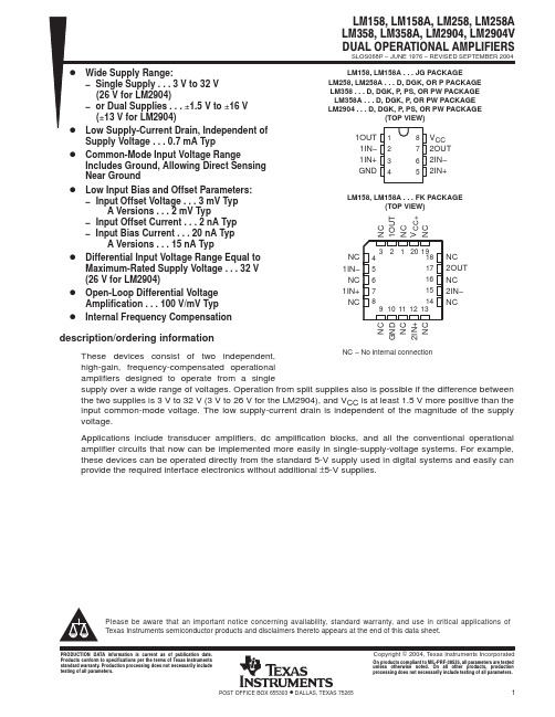
表面粗糙度学习资料 中文
表面粗糙度教材
完成记号 ~
表面粗糙度的标准数值
Ra
Rmax
Rz
0.2a
0.8S
0.8Z
1.6a
6.3S
6.3Z
6.3a
25S
25Z
25a
100S 100Z
无特别指定
由弊公司向客户・交易往来公司提供的技术资料,符合外为令附表的1 ~15项以及16 项所载技术。将符合外为令附表的技术提供给日本国非居住者时,需得到经济产业大 臣的许可。另外,将符合外为令附表16项的技术提供给日本国非居住者时,根据同项 所记载的发送区域以及Catch all货物管制所规定的内容,有个别情况需要得到经济产 业大臣的许可。在将本资料提供给非日本国居住者时,请留意以上注意点。
信息不全的图纸举例
100
φ 30.0 φ 30.0 φ 30.0
+0.2
φ30
-0.1
上・下面的真直度 如何
上・下面的平行度 如何
信息不全的图纸举例
适用的形体
公差的种类
记号
真直度的公差
单独形体
形状公差
平面度公差 真圆度公差 圆柱度公差
单独形体以及
线的轮廓度公差
关连形体
面的轮廓度公差
适用的形体 关连形体
9
最近与表面粗糙度有关的JIS
JIS B 0601:2001
(旧JIS B 0601:1994 表面粗糙度-定义及表示) 【改正】
产品几何量技术规范(GPS).表面结构:轮廓法.术语、定义和表面结构参数
ISO 4287:1997
Geometrical Product Specifications(GPS)-Surface texture: Profile method-Terms, definitions and surface texture
KIC 2000中文操作手册-1
KIC 2000爐溫測溫器1.啟動KIC 2000軟體KIC會自動在”開始”按鈕中添加一個快捷方式。
點擊這個圖標可啟動KIC 2000軟體。
進入下面畫面﹕1)此按鈕為總體設置(一次設好后,可不再修改):Units of Measure –有三個下拉選項Conveyor Speed, Distance, and Temperature.(選擇鏈條速度﹑距離﹑溫度單位)∙ Product Start Temperature –輸入產品開始測量時的最高溫度﹔實際測量時最好等SlimKIC2000及各個測溫點的溫度都低于此值時再開始測Profile.這樣和實際生產時的情況相一致.測出的曲線也比較准确.一般設為高于環境溫度5度。
測Profile 時當Air TC 的溫度在此基礎上變化超過2度時﹐SlimKIC 自動啟動﹐開始記錄數據∙ Profiling Hardware –選擇測溫方式(transmitter or datalogger)﹐無線傳輸或有線傳輸∙Languages –選擇語言(英語﹑西班牙語﹑德語﹑繁體﹑簡體和日本語 )﹐這些設置需配合電腦操作系統.如電腦的操作系統是簡體中文的,那就可以選擇簡體中文或英語,不管在什麼操作系統上,英語都是可選的.∙Engineer Password–選擇密碼2) 此按鈕為錫膏特性設置:Process Window Name–下拉菜單中選擇錫膏名稱或者人為輸入錫膏名稱Solder Paste Menu -進入錫膏數據庫,可從中選擇錫膏Edit S pecs–進入錫膏特性編輯Read only text box–顯示當前錫膏的specProcess Window Description–空白處輸入對此錫膏品種的一些注解∙Buttons at the Bottom of Screen–屏幕下方的按鈕錫膏品種數據庫∙綠色的勾表示接受所選的錫膏∙paste jar and tube提供此錫膏的廠商資料. ∙紅色 X取消您的選擇并退出編輯錫膏編輯升溫斜率和降溫斜率,斜率計算時間﹐預熱﹑浸泡﹑回流及最高溫等錫膏的一些特性綠色的勾表示保存并退出紅色 X表示放棄﹐不保存并退出Saving - Process Window保存–點擊綠色勾狀”保存并退出”按鈕 .接著會彈出右方對話框﹐問你是否要保存修改后的錫膏特性。
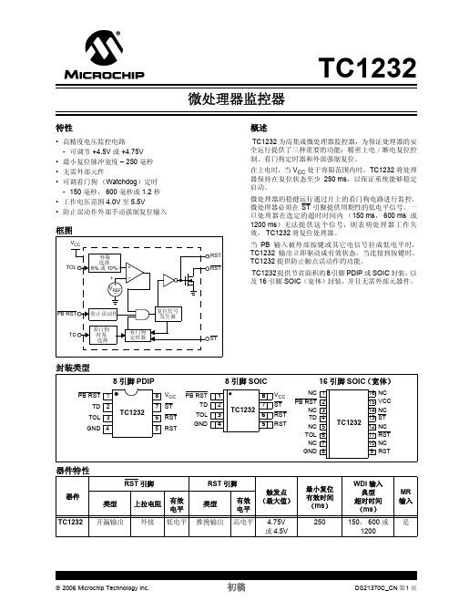
TC1232中文资料
2006 Microchip Technology Inc.
初稿
DS21370C_CN 第3 页
TC1232
tPB
ST
tST
tTD
PB RST
tPBD
VIL
RST RST
VIH tRST
防误动作 PB RST 输入引脚忽略长度小于 1 毫秒的输入脉冲 , 设计成只识别长度大于等于 20 毫秒的脉冲。
4: 由设计保证。
DS21370C_CN 第2 页
初稿
2006 Microchip Technology Inc.
TC1232
VCC
tF
+4.75V +4.25V
tR +4.75V
+4.25V
VCC = 5V
VCC
+4.5V(5% 触发点) +4.25V(10% 触发点) VCC
4.6V(5% 触发点) 4.5V(10% 触发点)
器件参考地。
复位输出 (高电平有效) 以下任一条件发生时,输出变成有效 (高电平):
1. 如果 VCC 电压跌落至选定的复位电压门限值以下; 2. 如果 PB RST 引脚被强制为低电平;
3. 如果 ST 引脚在选定的最小超时周期内没有被锁存; (参考 TD 引脚)
4. 初始上电时。
复位输出 (低电平有效) 以下任一条件发生时,输出变成有效 (低电平):
TC1232
微处理器监控器
特性
• 高精度电压监控电路 - 可调节 +4.5V 或 +4.75V
• 最小复位脉冲宽度 – 250 毫秒 • 无需外部元件 • 可调看门狗 (Watchdog)定时
- 1、下载文档前请自行甄别文档内容的完整性,平台不提供额外的编辑、内容补充、找答案等附加服务。
- 2、"仅部分预览"的文档,不可在线预览部分如存在完整性等问题,可反馈申请退款(可完整预览的文档不适用该条件!)。
- 3、如文档侵犯您的权益,请联系客服反馈,我们会尽快为您处理(人工客服工作时间:9:00-18:30)。
APPLICATIONS
FEATURES
5.1-Channel DVD Mini/Micro Component Systems Home Theater Stereo applications
BENEFITS
Class-T Architecture Audiophile Quality Sound 0.007% THD+N @ 30W 8Ω (with TP2050) High Efficiency 92% @ 60W 8Ω (with TP2050) Dynamic Range >100 dB
Note 1: Absolute Maximum Ratings indicate limits beyond which damage to the device may occur. See the table below for Operating Conditions.
Note 2: Human body model, 100pF discharged through a 1.5KΩ resistor.
OPERATING CONDITIONS
SYMBOL V5 VHI VLO TA Supply Voltage Logic Input High Logic Input Low Operating Temperature Range -40 25 PARAMETER MIN. 4.5 V5-1.0 1 85 TYP. 5 MAX. 5.5 UNITS V V V °C
R VN N SEN SE
V5
17 18 19 20
10k R O FA 500K R VPPSEN SE 20k
1 R O FB 5K
RCA J9
3
COF .1u;50V R O FA 500K CI 2.2u;10V RF 20K
V5
21 22 23
V5
FD BKN 1
7
O U T1A
O AO U T1 IN V1
TC 2000
R FBB
C FB
1 1
+
V5
RI 20K 1 R O FA 500K
JP
IN 1
2 2 1 R O FB 5K 2
R FBC FD BKP1 6
O U T1B
2
V5
24
MU TE
JU MPER
25 COF .1u;50V R O FA
C FB
O U T2B
4
TC2000 – KLI/1.1/12-03
元器件交易网
Tr i path Technol ogy, I nc. - Techni cal I nfor m ati on
E X T E R N A L C O M P O N E N T S D E S C R I P T I O N (Refer to the Application/Test Circuit)
Technical Information Revision 1.1 – December 2003
GENERAL DESCRIPTION
The TC2000 is a two channel audio controller that uses Tripath’s proprietary Digital Power Processing (DPPTM) technology. When combined with switching power output stages, the TC2000 allows the implementation of a complete Class-T audio amplifier. Class-T amplifiers offer both the audio fidelity of Class-AB and the power efficiency of Class-D amplifiers.
APPLICATION / TEST DIAGRAM
Inputs and TC2000
R R EF 8.2K
15 16
R EF OCD0 VN N SEN SE O VR LD B VPPSEN SE AG N D
OCD1 NC Y2 Y2B Y1B Y1 H MU TE
14 13 12 11 10 9 8 Y2 Y2B Y1B Y1 H MU TE R FBC
TC2000 AUDIO SIGNAL PROCESSOR PINOUT
BIASCAP FDBKP2 DCMP FDBKN2 VPW R FDBKP1 FDBKN1 HMUTE Y1 Y1B Y2B Y2 NC OCD2
1 2 3 4 5 6 7 8 9 10 11 12 13 14
28 27 26 25 24 23 22 21 20 19 18 17 16 15
元器件交易网
Tr i path Technol ogy, I nc. - Techni cal I nfor m ati on
TC2000 STEREO CLASS-T™ AUDIO CONTROLLER USING DIGITAL POWER PROCESSING (DPP™) TECHNOLOGY
RCA J10
26
3
BBM1 5 4
27 28
1 1
O AO U T2 IN V2
VPW R FD BKN 2
R FBC
O U T2A
+
CI 2.2u;10V
IN 2
2 2
RI 20K
V5 V5
R FBB
C FB
+
CS .1u;50V CS 100u;16V D C MP 3 R FBC FD BKP2 BIASC AP 2 1 R FBB C7 .1u;50V C FB
A B S O L U T E M A X I M U M R A T I N G S (Note 1)
SYMBOL V5 Vlogic TA TSTORE TJMAX ESDHB 5V Power Supply Input Logic Level Operating Free-air Temperature Range Storage Temperature Range Maximum Junction Temperature ESD Susceptibility – Human Body Model (Note 2), all pins PARAMETER Value 6 V5+0.3V -40 to 85 -55 to 150 150 2000 UNITS V V °C °C °C V
High fidelity, high efficiency Class-T Analog inputs
1
TC2000 – KLI/1.1/12-03
元器件交易网
Tr i path Technol ogy, I nc. - Techni cal I nfor m ati on
THERMAL CHARACTERISTICS
TC2000
SYMBOL θJA
PARAMETER Junction-to-ambient Thermal Resistance (still air)
Value 80
UNITS °C/W
ELECTRICAL CHARACTERISTICS
SYMBOL I5 fsw VIN VOUTHI VOUTLO RIN Supply Current Switching Frequency (adjustable via CFB) Input Sensitivity High Output Voltage Low Output Voltage Input Impedance Input DC Bias 2 2.5 600 0 V5-0.5 100 PARAMETER MIN. TYP. 60 650 1.5 MAX. UNITS mA kHz V V mV kΩ V
INV2 OAOUT2 BBM0 BBM1 MUTE INV1 OAOUT1 V5 AGND VPPSENSE OVRLDB VNNSENSE OCD1 REF
3
TC2000 – KLI/1.1/12-03
元器件交易网
Tr i path Technol ogy, I nc. - Techni cal I nfor m ati on
2
TC2000 – KLI/1.1/12-03
元器件交易网
Tr i path Technol ogy, I nc. - Techni cal I nfor m ati on
TC2000 AUDIO SIGNAL PROCESSOR PIN DESCRIPTIONS
Pin 1 2, 6 3 4, 7 5 8 9, 12 10, 11 13 14,16 15 17 18 19 20 21 22, 27 23, 28 24 25, 26 Function BIASCAP FDBKP2, FDBKP1 DCMP FDBKN2, FDBKN1 VPWR HMUTE Y1, Y2 Y1B, Y2B NC OCD2, OCD1 REF VNNSENSE OVRLDB VPPSENSE AGND V5 OAOUT1, OAOUT2 INV1, INV2 MUTE BBM1, BBM0 Description Bandgap reference times two (typically 2.5VDC). Used to set the common mode voltage for the input op amps. This pin is not capable of driving external circuitry. Positive switching feedback. Internal mode selection. This pin must be grounded for proper device operation. Negative switching feedback. Test pin. Must be left floating. Logic output. A logic high indicates both amplifiers are muted, due to the mute pin state, or a “fault”. Non-inverted switching modulator outputs. Inverted switching modulator outputs. No connect Over Current Detect. Ground if not used. Internal reference voltage; approximately 1.2 VDC. Negative power stage over/under supply voltage sense resistor tie point. A logic low output indicates the input signal has overloaded the amplifier. Positive power stage over/under supply voltage sense resistor tie point. Ground 5 Volt power supply input. Input stage output pins. Single-ended inputs. Inputs are a “virtual” ground of an inverting opamp with approximately 2.4VDC bias. When set to logic high, both amplifiers are muted and in idle mode. When low (grounded), both amplifiers are fully operational. If left floating, the device stays in the mute mode. Ground if not used. Break-before-make timing control.