DRV8842PWP;DRV8842PWPR;中文规格书,Datasheet资料
QX6104中文规格书
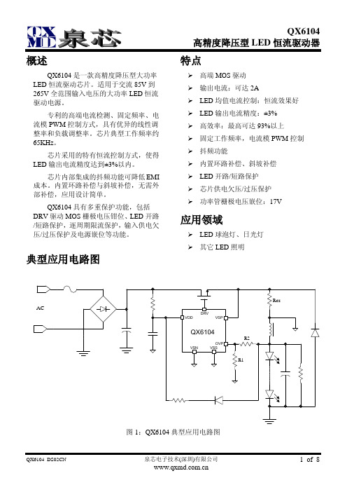
.典型应用电路图图1:QX6104典型应用电路图概述 QX6104是一款高精度降压型大功率LED 恒流驱动芯片。
适用于交流85V 到265V 全范围输入电压的大功率LED 恒流驱动电源。
专利的高端电流检测、固定频率、电流模PWM 控制方式,具有优异的线性调整率和负载调整率。
芯片典型工作频率约65KHz 。
芯片采用的特有恒流控制方式,使得LED 输出电流精度达到±3%以内。
芯片内部集成的抖频功能可降低EMI 成本。
内置环路补偿与斜坡补偿,无需外部补偿,应用设计简单。
QX6104具有多重保护功能,包括DRV 驱动MOS 栅极电压钳位、LED 开路/短路保护,逐周期限流保护,输入供电欠压/过压保护及电源嵌位等功能。
特点高端MOS 驱动 输出电流:可达2ALED 均值电流控制:恒流效果好 LED 输出电流精度:±3%高效率:最高可达93%以上固定工作频率,电流模PWM 控制 抖频功能内置环路补偿、斜坡补偿 LED 开路/短路保护 芯片供电欠压/过压保护 功率管栅极电压嵌位:17V 应用领域 LED 球泡灯、日光灯 其它LED 照明订货信息产品型号QX6104丝印6104X批号封装及管脚分配DRVVSN VSPOVPVDD132645VSS6104XSOT23-6管脚描述内部电路方框图DRVVSPVSN图2:QX6104内部电路方框图极限参数(注1)注1:超过上表中规定的极限参数会导致器件永久性损坏。
而工作在以上极限条件下可能会影响器件的可靠性。
电气特性除非特别说明,T A =25o C电气特性(接上一页) 除非特别说明,T A =25o C应用指南概述QX6104是一款高精度降压型大功率LED 恒流驱动芯片,输出电流可达2A 以上。
芯片采用专利的高端电流检测、固定频率、电流模PWM 控制方式,具有优异的线性调整率和负载调整率。
芯片内置频率补偿与斜坡补偿,无需外部补偿。
QX6104还集成了抖频功能,以改善系统的EMI 特性。
Rockwell Automation Trusted 8 Channel Temperature

PD-T8840 TrustedTrusted 8 Channel Temperature FTAProduct OverviewThe Trusted® Temperature Field Termination Assembly (FTA) is designed to interface between a Trusted system and up to eight temperature, voltage or current devices using a range of available plug in conditioning units.Features:•Eight Input channels per Trusted Temperature FTA.•Flexible user defined conditioning.•Standard DIN rail compatibility.•Configurable 2 or 3 wire Resistance Temperature Detector (RTD) inputs.•Dual 24 V Supply.Trusted PD-T8840Page intentionally left blankPREFACEIn no event will Rockwell Automation be responsible or liable for indirect or consequential damages resulting from the use or application of this equipment. The examples given in this manual are included solely for illustrative purposes. Because of the many variables and requirements related to any particular installation, Rockwell Automation does not assume responsibility or reliability for actual use based on the examples and diagrams.No patent liability is assumed by Rockwell Automation, with respect to use of information, circuits, equipment, or software described in this manual.All trademarks are acknowledged.DISCLAIMERIt is not intended that the information in this publication covers every possible detail about the construction, operation, or maintenance of a control system installation. You should also refer to your own local (or supplied) system safety manual, installation and operator/maintenance manuals.REVISION AND UPDATING POLICYThis document is based on information available at the time of its publication. The document contents are subject to change from time to time. The latest versions of the manuals are available at the Rockwell Automation Literature Library under "Product Information" information "Critical Process Control & Safety Systems".TRUSTED RELEASEThis technical manual applies to Trusted Release: 3.6.1.LATEST PRODUCT INFORMATIONFor the latest information about this product review the Product Notifications and Technical Notes issued by technical support. Product Notifications and product support are available at the Rockwell Automation Support Centre atAt the Search Knowledgebase tab select the option "By Product" then scroll down and select the Trusted product.Some of the Answer ID’s in the Knowledge Base require a TechConnect Support Contract. For more information about TechConnect Support Contract Access Level and Features please click on the following link:https:///app/answers/detail/a_id/50871This will get you to the login page where you must enter your login details.IMPORTANT A login is required to access the link. If you do not have an account then you can create one using the "Sign Up" link at the top right of the web page.DOCUMENTATION FEEDBACKYour comments help us to write better user documentation. If you discover an error, or have a suggestion on how to make this publication better, send your comment to our technical support group at SCOPEThis manual specifies the maintenance requirements and describes the procedures to assist troubleshooting and maintenance of a Trusted system. WHO SHOULD USE THIS MANUALThis manual is for plant maintenance personnel who are experienced in the operation and maintenance of electronic equipment and are trained to work with safety systems. SYMBOLSIn this manual we will use these notices to tell you about safety considerations.SHOCK HAZARD: Identifies an electrical shock hazard. If a warning label is fitted, it can be on or inside the equipment.WARNING: Identifies information about practices or circumstances that can cause an explosion in a hazardous environment, which can cause injury or death, property damage or economic loss.ATTENTION: Identifies information about practices or circumstances that can cause injury or death.CAUTION: Identifies information about practices or circumstances that can cause property damage or economic loss.BURN HAZARD: Identifies where a surface can reach dangerous temperatures. If a warning label is fitted, it can be on or inside the equipment.This symbol identifies items which must be thought about and put in place when designing and assembling a Trusted controller for use in a Safety Instrumented Function (SIF). It appears extensively in the Trusted Safety Manual.IMPORTANTIdentifies information that is critical for successful application and understanding of the product.NOTE Provides key information about the product or service.TIP Tips give helpful information about using or setting up the equipment.WARNINGS AND CAUTIONSWARNING: EXPLOSION RISKDo not connect or disconnect equipment while the circuit is live or unless the area is known to be free of ignitable concentrations or equivalentAVERTISSEMENT - RISQUE D’EXPLOSIONNe pas connecter ou déconnecter l’équipement alors qu’il est sous tension, sauf si l’environnement est exempt de concentrations inflammables ou équivalenteMAINTENANCEMaintenance must be carried out only by qualified personnel. Failure to follow these instructions may result in personal injury.CAUTION: RADIO FREQUENCY INTERFERENCEMost electronic equipment is influenced by Radio Frequency Interference. Caution should be exercised with regard to the use of portable communications equipment around such equipment. Signs should be posted in the vicinity of the equipment cautioning against the use of portable communications equipment.CAUTION:The module PCBs contains static sensitive components. Static handling precautions must be observed. DO NOT touch exposed connector pins or attempt to dismantle a module.ISSUE RECORDIssue Date Comments1 July 052 Aug 06 Corrections3 Jun 08 Open circuit effects4 Apr 10 Change to sub-section 2.15 Apr 16 Rebranded, reformatted, Inclusion of IEEE symbols and correction oftypographical errorsPage intentionally left blankTrusted 8 Channel Temperature FTA Table of Contents Table of Contents1.Description (3)2.Installation (5)2.1. Cable Selection (5)2.2. Module Pin-out Connections (7)2.2.1. RTD1 to RTD8 (7)2.2.2. PWR (7)2.2.3. IOIF (8)3.Applications (9)3.1. Signal Conditioning units (9)3.1.1. Isolator Physical dimensions (9)3.1.2. Conditioning Unit Specification (10)3.1.3. Available Conditioning Units (10)3.1.4. Cold Junction Compensation (12)4.Specifications (13)Table of Contents Trusted 8 Channel Temperature FTAPage intentionally left blank1.DescriptionFigure 1 Trusted Temperature FTAThe Trusted Temperature FTA enables connection to 8 temperature, voltage or current devices using RTD, Thermocouple, Voltage and Current input conditioning units. The Trusted Temperature FTA excludes the conditioning units to allow maximum configurability. More than one type of conditioning unit can be used on the same FTA.Figure 2 Module Layout2. Installation2.1. Cable SelectionThe Trusted Temperature FTA can connect direct to an Analogue Input Module using either companion cables TC-211/212 or SmartSlot cables TC-511/512. The Output can also be connected to the Analogue Input module via a Versatile Field Termination Assembly (VFTA) if necessary to be compatible with an existing installation.Some isolator modules will float their output to 10 V on an open circuit field input. This will cause slice faults on the analogue input module. If the isolator output is connected to the module via a 250 Ω resistor on a VFTA, the voltage will be pulled down into the module’s operating range. Therefore even if the isolator output is a voltage signal, it is recommended to connect the input via a VFTA with the 250 Ω VFTA resistor in parallel.Figure 3 System Connectivity using 1-5 V Output DevicesAnalogue module 8431/ 8432Temperature FTA 8840Temperature FTA 8840 Temperature FTA 8840Temperature FTA 8840Temperature FTA 8840TC-211/212Typical Configuration using conditioning devices with 1-5 V outputUp to 8 temperature devicesFigure 4 System Connectivity using VFTAFor signal conditioning units that provide signals as 4 mA to 20 mA for low to highengineering range, a conversion is needed because the voltage measured by the module input is not exactly 1 V to 5 V.EU = ((count/4036.5) – 0.007828) x (HEU – LEU) + LEU Where:LEU = Low engineering unit range HEU = High engineering unit range Count = Raw value seen by input EU = Engineering unit valueFor signal conditioning units that provide a voltage signal of 1 V to 5 V, no special factors are required:EU = (count/4096) x (HEU – LEU) + LEU.VFTA 8842Temperature FTA 8840 Temperature FTA 8840 Temperature FTA 8840Temperature FTA 8840Temperature FTA 8840Typical Configuration using conditioning Devices with 1 to 5 V outputusing a VFTAUp to 8 temperature devicesAnalogue module 84312.2.Module Pin-out Connections 2.2.1.RTD1 to RTD8Terminal Description ConditioningModule Pin Thermocoupleor Voltage2 wireRTD3 wireRTD4 wireRTDR Sense Input (X) 0 Red Red R Input Low (-) 2 - Red Red Red W Input High (+) 1 + White White White/WhiteTable 1 Input TerminationsFigure 5 Temperature Input Schematic2.2.2.PWRTerminal Description+ 24 Vdc- 0 V- 0 V+ 24 VdcTable 2 Power TerminationsThere are no fuses fitted to the power rails on the Trusted Temperature FTA. External 2 A fuses should be fitted to the power wiring.2.2.3.IOIFTerminal Description1 0 V2 Output, channel 13 Output, channel 24 Output, channel 35 Output, channel 46 Output, channel 57 Output, channel 68 Output, channel 79 Output, channel 810 0 VTable 3 Temperature Signal Outputs3.ApplicationsThe Trusted Temperature FTA interfaces between a Trusted system and up to eight monitoring devices using, isolated RTD, Thermocouple, Voltage and Current input conditioning units. Compatible conditioning units must have 1 V to 5 V outputs.3.1.Signal Conditioning unitsCompatible conditioning unit include the 7B series of units from Analog Devices Inc and SCM7B series from Dataforth.3.1.1.Isolator Physical dimensionsFigure 6 Conditioning Unit Dimensions3.1.2.Conditioning Unit SpecificationThe following specification applies to all signal conditioning unit types Operating Voltage Range15 Vdc to 30 Vdc Power consumption 2 W maxOperating Temperature -40 °C to +85 °C Common mode Isolation 1500 Vac rms Continuous field voltage withstand 120 Vac rmsAccuracy ±0.3 % spanOutput Signal range +1 V to +5 V3.1.3.Available Conditioning UnitsInput Types Range ModelNumber (A)Model Number (B)Isolated Voltage0 mV to +10 mV7B30-01-1SCM7B30-010 mV to +100 mV7B30-02-1SCM7B30-020 V to +1 V7B30-03-1SCM7B30-03+1 V to +5 V7B30-05-1SCM7B30-04-10 mV to +10 mV7B30-06-1SCM7B30-05-100 mV to +100 mV7B30-07-1SCM7B30-06-1 V to +1 V7B30-08-1SCM7B30-070 V to 10 V Not available SCM7B30-08-5 V to +5 V Not available SCM7B31-01-10 V to +10 V Not available SCM7B31-020 V to 5 V Not available SCM7B31-03 Isolated Current 4 mA to 20 mA7B32-01-1SCM7B32-010 mA to 20 mA Not available SCM7B32-02 Isolated RTD-100 °C to +100 °C (-148 °F to +212 °F)7B34-01-1SCM7B34-01Number (A)Number (B) Pt 100 ΩLinearized0 °C to +100 °C (+32 °F to +21 2 °F)7B34-02-1SCM7B34-020 °C to +200 °C (+32 °F to +392 °F)7B34-03-1SCM7B34-030 °C to +600 °C (+32 °F to +1112 °F)7B34-04-1SCM7B34-04-50 °C to +350 °C (-58 °F to +662 °F)7B34-05-1SCM7B34-05Isolated RTD Ni 120 ΩLinearized 0 °C to +300 °C (+32 °F to +572 °F)7B34-N-01-1SCM7B34N-01 0 °C to +200 °C (+32 °F to +392 °F)7B34-N-02-1SCM7B34N-02Isolated 2 wireTransmitter(inc loop power)4 mA to 20 mA7B35-01-1SCM7B35-01Isolated Potentiometer 0 Ω to 100 ΩNot available SCM7B36-01 0 Ω to 200 ΩNot available SCM7B36-02 0 Ω to 500 ΩNot available SCM7B36-03 0 Ω to 1 KΩNot available SCM7B36-04 0 Ω to 5 KΩNot available SCM7B36-05 0 Ω to 10 KΩNot available SCM7B36-06Isolated Thermocouple Type J -100 °C to +760 °C (-148 °F to +1400 °F)7B37-J-01-1SCM7B37J-01 0 °C to +200 °C (+32 °F to +392 °F)7B37-J-10-1SCM7B37J-10 0 °C to +400 °C (+32 °F to +752 °F)7B37-J-11-1SCM7B37J-11 0 °C to +600 °C (+32 °F to +1112 °F)7B37-J-12-1SCM7B37J-12 +300 °C to +600 °C (+572 °F to +1112 °F)7B37-J-13-1SCM7B37J-13Isolated Thermocouple Type K -100 °C to +1350 °C (-148 °F to +2462 °F)7B37-K-02-1SCM7B37K-02 0 °C to +300 °C (+32 °F to +572 °F)7B37-K-20-1SCM7B37K-20 0 °C to +600 °C (+32 °F to +1112 °F)7B37-K-21-1SCM7B37K-21 0 °C to +1200 °C (+32 °F to +2192 °F)7B37-K-22-1SCM7B37K-22 +600 °C to +1200 °C (+1112 °F to +2192 °F)7B37-K-23-1SCM7B37K-23Number (A)Number (B)Isolated Thermocouple Type J Linearized 0 °C to +760 °C (+32 °F to +1400 °F)7B47-J-01-1SCM7B47J-01 -100 °C to +300 °C (-148 °F to +572 °F)7B47-J-02-1SCM7B47J-02Isolated Thermocouple Type K Linearized 0 °C to +1300 °C (+32 °F to +2372 °F)7B47-K-03-1SCM7B47K-03 0 °C to +600 °C (+32 °F to +1112 °F)7B47-K-04-1SCM7B47K-04Table 4 Available Conditioning UnitsAdditional standard ranges, including custom are available. Information and datasheets can be supplied upon request.3.1.4.Cold Junction CompensationThe Trusted Temperature FTA includes a Cold Junction Compensation (CJC) resistor for each of the inputs. This makes the FTA compatible with Thermocouple conditioning units. For information in determining compatible Thermocouple Units the CJC resistor specification is as follows:GE Thermometrics Part D95G104WNTC, 100 K at 25 °CFor further information see the manufacturer’s data sheet.Trusted 8 Channel Temperature FTA 4. Specifications 4.SpecificationsVoltage Range 15 Vdc to 30 VdcMaximum Input Current 2.5 ANumber of Inputs 8Input types Voltage, Current, RTD and Thermocoupledepending on chosen conditioning unit. Environmental Specifications Refer to Document 552517DimensionsHeight 110 mm (4.3 in)Width 145 mm (5.7 in)Depth 68 mm (2.6 in)Depth with conditioning unit fitted 90 mm (3.6 in)Weight 248 g (0.55 lb)Accuracy, resolution Dependant on conditioning unitRockwell Automation Publication PD-T8840 Issue 5 13。
XLSEMI XL8002 80V 1A高效降压PWM LED常电流驱动器说明书
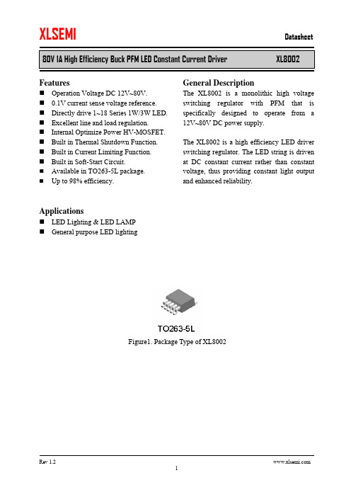
80V 1A High Efficiency Buck PFM LED Constant Current Driver XL8002FeaturesOperation Voltage DC 12V~80V. 0.1V current sense voltage reference. Directly drive 1~18 Series 1W/3W LED. Excellent line and load regulation.Internal Optimize Power HV-MOSFET. Built in Thermal Shutdown Function. Built in Current Limiting Function.Built in Soft-Start Circuit.Available in TO263-5L package. Up to 98% efficiency. ApplicationsLED Lighting & LED LAMP General purpose LED lightingGeneral DescriptionThe XL8002 is a monolithic high voltage switching regulator with PFM that is specifically designed to operate from a 12V~80V DC power supply.The XL8002 is a high efficiency LED driver switching regulator. The LED string is driven at DC constant current rather than constant voltage, thus providing constant light output and enhanced reliability.Figure1. Package Type of XL800280V 1A High Efficiency Buck PFM LED Constant Current Driver XL800280V 1A High Efficiency Buck PFM LED Constant Current Driver XL8002Figure4. XL8002 Typical Application80V 1A High Efficiency Buck PFM LED Constant Current Driver XL8002Figure5. Efficiency VS Output N*1W LEDFigure6. Output ILED Load Regulation VS Output N*1W LED80V 1A High Efficiency Buck PFM LED Constant Current Driver XL800280V 1A High Efficiency Buck PFM LED Constant Current Driver XL800280V 1A High Efficiency Buck PFM LED Constant Current Driver XL8002 Figure7. XL8002 System Application at VIN=60V~80V Schematic Figure8. XL8002 System Application at VIN=60V~80V Efficiency Curve80V 1A High Efficiency Buck PFM LED Constant Current Driver XL8002 Figure9. XL8002 System Application at VIN=36V~60V Schematic80V 1A High Efficiency Buck PFM LED Constant Current Driver XL8002Figure10. XL8002 System Application at VIN=36V~60V Efficiency Curve Table2: Figure9 Input VIN=36V/48V system parameters table:80V 1A High Efficiency Buck PFM LED Constant Current Driver XL8002Figure11. XL8002 System Application at VIN=12V~36V SchematicFigure12. XL8002 System Application at VIN=12V~36V Efficiency CurveTable3: Figure11 Input VIN=12V/24V system parameters table:VIN=12V VIN=24VFOSC Pout Efficiency FOSC Pout Efficiency1.01W 82.3%1.96W 90.8%2.91W 94.1%47.25K 3.80W 95.5%42.17K 4.70W 96.6%31.13K 5.61W 97.2%80V 1A High Efficiency Buck PFM LED Constant Current Driver XL8002 Figure13. XL8002 System Application at VIN=60V~80V Schematic Figure14. XL8002 System Application at VIN=60V~80V Efficiency Curve80V 1A High Efficiency Buck PFM LED Constant Current Driver XL800280V 1A High Efficiency Buck PFM LED Constant Current Driver XL8002。
RS PRO IPM 242 600A 电流探头测试仪说明书

ENGLSpecifications: (All at 23℃±5℃, ≦80% R.H.)DC/AC VoltageDC/AC VoltageFunction Range Accuracy*DCV 99.99V± (0.7% + 2dgt) 999.9VACV 99.99V ± (1.0% + 5dgt)50 ~ 500Hz 999.9VLPF ACV 99.99V 50 ~ 60Hz ± (1% + 5dgt)>60 ~ 400Hz ± (5% + 5dgt) 999.9V* DCV <1000dgt, add 6 dgt to the accuracy.ACV <1000dgt, add 3 dgt to the accuracy.Overload Protection: 1000VrmsInput Impedance:3.5MΩ // <100pFAC+DC V RMS Accuracy: same as ACV spec. +DCV spec.AC CurrentAC CurrentFunction Range AccuracyACA 99.99A 50 ~ 60Hz ± (1.5% + 5dgt) **>60 ~ 400Hz ± (2% + 5dgt) ** 599.9ALPF ACA 0.10A ~ 99.99A 50 ~ 60Hz ± (1.5% + 5dgt) **>60 ~ 400Hz ± (5% + 5dgt) ** 599.9A** The measured value <1000dgt, add 5 dgt to the accuracy. Overload Protection: 600ArmsPeak Hold (Peak MAX / Peak MIN)Peak Hold : Peak MAX / Peak MIN Function Range AccuracyACV 140.0V± (3.0% + 15dgt) 1400VACA 140.0A± (3.0% + 15dgt) 850AOverload Protection: 1000 V RMS, 600 Arms FrequencyFrequencyFunction Range AccuracyFrequency20.00 ~ 99.99Hz± (0.5% + 3dgt) 20.0 ~ 999.9Hz0.020 ~ 9.999KHzOverload Protection: 1000 V RMS, 600 Arms Harmonic DistortionTotal Harmonic DistortionFunction Range AccuracyACA /ACV 99.9% ± (3.0% + 10dgt)Harmonic distortion measurement Harmonic order Range AccuracyH01 ~ H1299.9% ± (5% + 10dgt)H13 ~ H25 ± (10% + 10dgt)Overload Protection: 1000 V RMS, 600 Arms-If ACV<10Vrms or ACA <10Arms, it will display “rdy”.-If the fundamental frequency out of range 45 ~ 65Hz, it will display “out.F”.Inrush CurrentInrush Current :Function Range AccuracyACA 99.99A ± (2.5% + 0.2A) 599.9A ± (2.5% + 5dgt)Overload Protection: 1000 V RMS, 600 ArmsAccuracy defined for:Sine wave, ACA≧10Arms, Freq. 50/60Hz- Integration time about 100m secActive Power (AC)Active Power (AC)Function Range AccuracyACW 9.999 kW**A,error×V,reading+V,error×A,reading 99.99 kW599.9KW** The measured value<1.000kW,add 10 dgt to the accuracy.Overload Protection: 1000 V RMS, 600 ArmsAccuracy defined for:ACW : Sine wave , ACV≧10 V RMS, ACA≧5 ArmsFreq. 50~60Hz, PF=1.00Power FactorPower FactorFunction Range Accuracy* PF-1.00 ~ 0.00 ~1.00 ±3°±1dgt * ACA<100A, add ±2° to the accuracyOverload Protection: 1000 V RMS, 600 ArmsResistance & Continuity & DiodeResistance & Continuity & Diode Function Range AccuracyResistance 999.9 Ω± (1.0% + 5dgt) 9.999 kΩ± (1.0% + 3dgt) 99.99 kΩContinuity 999.9 Ω± (1.0% + 5dgt)Diode 0.40~ 0.80V ± 0.1V Overload Protection: 1000VrmsMax. Test Current: Approx. 0.5mA.Continuity Check: <30Ω Beep On.>100Ω Beep OFF.Continuity Indicator: 2 KHz Tone BuzzerContinuity Response Time: < 100ms. CapacitanceCapacitanceFunction Range AccuracyCapacitance 3.999 μF± (1.9% + 8dgt) 39.99 μF399.9 μF3999 μFOverload Protection: 1000 V RMS TemperatureTemperatureFunction Range Accuracy°C-50 °C ~ 99.9 °C ± (1% + 2°C)100 °C ~ 399.9 °C400 °C ~ 1000 °C± (1% + 1°C)°F-58 °F ~ 211.9 °F ± (1% + 4°F)212.0 °F ~ 751.9 °F752 °F ~ 1832 °F± (1% + 2°F)Overload Protection: 1000 V RMS。
福禄克 884xa系列台式万用表手册

有限担保和有限责任
Fluke 担保在正常使用和保养的情况下,其产品没有材料和工艺上的缺陷。从寄送之日起,担保期为三年。部ቤተ መጻሕፍቲ ባይዱ件、产品修理和服务的担保期限为 90 天。本担保仅限于 Fluke 授权零售商的原购买人或最终用户,并且不适 用于一次性电池、电缆接头、电缆绝缘转换接头或 Fluke 认为由于误用、改装、疏忽、污染及意外或异常操 作或处理引起的任何产品损坏。Fluke 担保软件能依照功能规格正常运行 90 天,并且软件是记录在无缺陷的 媒介上。Fluke 并不担保软件毫无错误或在运行中不会中断。
Fluke Europe B.V. P.O. Box 1186 5602 BD Eindhoven The Netherlands
11/99
要在线 注册您的产 品,请 请 请 。
目录
章节 1
标题
页
章概述和技术指标.................................................................................. 1-1
®
8845A/8846A Digital Multimeter
用户手册
July 2006, Rev. 3, 3/11 (Simplified Chinese)
© 2006 - 2011 Fluke Corporation. Specifications subject to change without notice. All rights reserved. All product names are trademarks of their respective companies.
概述 ....................................................................................................... 1-3 用户文件 ................................................................................................ 1-3 关于本手册 ............................................................................................ 1-3 安全信息 ................................................................................................ 1-4
ISL8841AABZ资料
Features
• 1A MOSFET gate driver • 90μA start-up current, 125μA maximum • 35ns propagation delay current sense to output • Fast transient response with peak current mode control • 30V operation • Adjustable switching frequency to 2MHz • 20ns rise and fall times with 1nF output load • Trimmed timing capacitor discharge current for accurate deadtime/maximum duty cycle control • 1.5MHz bandwidth error amplifier • Tight tolerance voltage reference over line, load and temperature • ±3% current limit threshold • Pb-free plus anneal available and ELV, WEEE, RoHS Compliant
GND
2.5V
A = 0.5
CS
FB
+ -
ERROR AMPLIFIER
VF TOTAL = 1.15V
COMP
VREF
100k
2.9V 1.0V
150k
OSCILLATOR COMPARATOR <10ns
RTCT
+
8.4mA
ON
FN6320.3 April 18, 2007
ISL8844A中文资料

PART NUMBER ISL8840A ISL8841A ISL8842A ISL8843A ISL8844A ISL8845A
RISING UVLO 7.0 7.0
14.4V 8.4V 14.4V 8.4V
MAX. DUTY CYCLE 100% 50% 100% 100% 50% 50%
Pinout
1
CAUTION: These devices are sensitive to electrostatic discharge; follow proper IC Handling Procedures.
1-888-INTERSIL or 1-888-468-3774 | Intersil (and design) is a registered trademark of Intersil Americas Inc.
deadtime/maximum duty cycle control • 1.5MHz bandwidth error amplifier • Tight tolerance voltage reference over line, load and
temperature • ±3% current limit threshold • Pb-free plus anneal available and ELV, WEEE, RoHS
ISL8843AMBZ 8843 AMBZ -55 to +125 8 Ld SOIC M8.15 (See Note)
ISL8843AMUZ 43AMZ (See Note)
-55 to +125 8 Ld MSOP M8.118
ISL8844AABZ 8844 AABZ -40 to +105 8 Ld SOIC M8.15 (See Note)
DRV8818PWP;DRV8818PWPR;DRV8818EVM;中文规格书,Datasheet资料

DRV8818 SLVSAX9A–SEPTEMBER2011–REVISED FEBRUARY2012STEPPER MOTOR CONTROLLER ICCheck for Samples:DRV8818FEATURES•Pulse Width Modulation(PWM)Microstepping Lower R ds(on)Motor Driver•Thermally Enhanced Surface Mount Package –Built-In Microstepping IndexerAPPLICATIONS–Up to2.5-A Current Per Winding•Printers–Microstepping Indexer Provides up to1/8-Step Operation•Textile Machinery–Low0.37-Ω(HS+LS)MOSFET•Positioning/TrackingOn-Resistance(at25°)•Factory Automation–Programmable Mixed Decay,Blanking,and•RoboticsOff Time•Pin-Compatible Upgrade to DRV8811WithDESCRIPTION/ORDERING INFORMATIONThe DRV8818provides an integrated stepper motor driver solution for printers,scanners,and other automated equipment applications.The device has two H-bridge drivers,as well as microstepping indexer logic to control a stepper motor.The output driver block for each consists of N-channel power MOSFETs configured as full H-bridges to drive the motor windings.A simple step/direction interface allows easy interfacing to controller circuits.Pins allow configuration of the motor in full-step,half-step,quarter-step,or eighth-step modes.Decay mode and PWM off time are programmable.Internal shutdown functions are provided for over current protection,short circuit protection,under-voltage lockout and overtemperature.The DRV8818is packaged in a PowerPAD™28-pin HTSSOP package with PowerPAD™(Eco-friendly:RoHS and no Sb/Br).ORDERING INFORMATION(1)PACKAGE(2)ORDERABLE PART NUMBER TOP-SIDE MARKINGReel of2000DRV8818PWPRPowerPAD™(HTSSOP)–PWP DRV8818Tube of50DRV8818PWP(1)For the most current package and ordering information,see the Package Option Addendum at the end of this document,or see the TIweb site at .(2)Package drawings,thermal data,and symbolization are available at /packaging.Please be aware that an important notice concerning availability,standard warranty,and use in critical applications of TexasInstruments semiconductor products and disclaimers thereto appears at the end of this data sheet.PowerPAD is a trademark of Texas Instruments.DRV8818SLVSAX9A–SEPTEMBER2011–REVISED FUNCTIONAL BLOCK DIAGRAMDRV8818 SLVSAX9A–SEPTEMBER2011–REVISED FEBRUARY2012TERMINAL FUNCTIONSNAME NO.I/O(1)DESCRIPTION EXTERNAL COMPONENTS OR CONNECTIONSPOWER AND GROUNDGND7,21-Device groundVMA28-Bridge A power supply Connect to motor supply(8V to35V).Both pins must be connectedto same supply.VMB15-Bridge B power supply Connect to motor supply(8V to35V).Both pins must be connectedto same supply.VCC10-Logic supply voltage Connect to3-V to5-V logic supply.Bypass to GND with a0.1-μFceramic capacitor.CP123IO Charge pump flying capacitor Connect a0.22-μF capacitor between CP1and CP2.CP224IO Charge pump flying capacitor Connect a0.22-μF capacitor between CP1and CP2.VCP22IO High-side gate drive voltage Connect a0.22-μF ceramic capacitor to V M.VGD20IO Low-side gate drive voltage Bypass to GND with a0.22-μF ceramic capacitor.CONTROLENABLEn26I Enable input Logic high to disable device outputs,logic low to enable outputs.Weak internal pullup to VCC.SLEEPn27I Sleep mode input Logic high to enable device,logic low to enter low-power sleep mode.Weak internal pulldown.DECAY5I Decay mode select Voltage applied sets decay mode-see motor driver description fordetails.Bypass to GND with a0.1-μF ceramic capacitor.Weakinternal pulldown.STEP19I Step input Rising edge causes the indexer to move one step.Weak internalpulldown.DIR3I Direction input Level sets the direction of stepping.Weak internal pulldown.USM013I Microstep mode0USM0and USM1set the step mode-full step,half step,quarterstep,or eight microsteps/step.Weak internal pulldown.USM112I Microstep mode1USM0and USM1set the step mode-full step,half step,quarterstep,or eight microsteps/step.Weak internal pulldown.RESETn17I Reset input Active-low reset input initializes the indexer logic and disables theH-bridge outputs.Weak internal pullup to VCC.SRn16I Sync.Rect.enable input When active low,synchronous rectification is enabled.Weak internalpulldown.VREF8I Current set reference input Reference voltage for winding current setRCA6I Bridge A blanking and off time adjust Connect a parallel resistor and capacitor to GND-see motor driverdescription for details.RCB9I Bridge B blanking and off time adjust Connect a parallel resistor and capacitor to GND-see motor driverdescription for details.ISENA1-Bridge A ground/Isense Connect to current sense resistor for bridge AISENB14-Bridge B ground/Isense Connect to current sense resistor for bridge BOUTPUTSAOUT14O Bridge A output1Connect to bipolar stepper motor windingAOUT225O Bridge A output2Positive current is AOUT1→AOUT2BOUT111O Bridge B output1Connect to bipolar stepper motor windingBOUT218O Bridge B output2Positive current is BOUT1→BOUT2HOMEn2O Home position Logic low when at home state of step table,logic high at other states (1)Directions:I=input,O=output,OZ=3-state output,OD=open-drain output,IO=input/outputISENAHOMEDIRAOUT1DECAYRCAGNDVREFRCBVCCBOUT1USM1USM0ISENBVMASLEEPnENABLEnAOUT2CP2CP1VCPGNDVGDSTEPBOUT2RESETnSRnVMBDRV8818SLVSAX9A–SEPTEMBER2011–REVISED ABSOLUTE MAXIMUM RATINGS(1)(2)(3)MIN MAX UNIT V MX Power supply voltage range–0.335VV CC Power supply voltage range–0.37V Digital pin voltage range–0.57VV REF Input voltage range–0.3V V CC V ISENSEx pin voltage range–0.30.5VI O(peak)Peak motor drive output current Internally limitedP D Continuous total power dissipation See Thermal Information table T J Operating junction temperature range–40150°CT stg Storage temperature range–60150°C (1)Stresses beyond those listed under"absolute maximum ratings"may cause permanent damage to the device.These are stress ratingsonly,and functional operation of the device at these or any other conditions beyond those indicated under"recommended operating conditions"is not implied.Exposure to absolute–maximum–rated conditions for extended periods may affect device reliability.(2)All voltage values are with respect to network ground terminal.(3)Power dissipation and thermal limits must be observed.THERMAL INFORMATIONDRV8818THERMAL METRIC(1)PWP UNITS28PINSθJA Junction-to-ambient thermal resistance(2)32.2θJCtop Junction-to-case(top)thermal resistance(3)16.3θJB Junction-to-board thermal resistance(4)14°C/WψJT Junction-to-top characterization parameter(5)0.5ψJB Junction-to-board characterization parameter(6)13.8θJCbot Junction-to-case(bottom)thermal resistance(7) 2.1(1)For more information about traditional and new thermal metrics,see the IC Package Thermal Metrics application report,SPRA953.(2)The junction-to-ambient thermal resistance under natural convection is obtained in a simulation on a JEDEC-standard,high-K board,asspecified in JESD51-7,in an environment described in JESD51-2a.(3)The junction-to-case(top)thermal resistance is obtained by simulating a cold plate test on the package top.No specificJEDEC-standard test exists,but a close description can be found in the ANSI SEMI standard G30-88.(4)The junction-to-board thermal resistance is obtained by simulating in an environment with a ring cold plate fixture to control the PCBtemperature,as described in JESD51-8.(5)The junction-to-top characterization parameter,ψJT,estimates the junction temperature of a device in a real system and is extractedfrom the simulation data for obtainingθJA,using a procedure described in JESD51-2a(sections6and7).(6)The junction-to-board characterization parameter,ψJB,estimates the junction temperature of a device in a real system and is extractedfrom the simulation data for obtainingθJA,using a procedure described in JESD51-2a(sections6and7).(7)The junction-to-case(bottom)thermal resistance is obtained by simulating a cold plate test on the exposed(power)pad.No specificJEDEC standard test exists,but a close description can be found in the ANSI SEMI standard G30-88.DRV8818 SLVSAX9A–SEPTEMBER2011–REVISED FEBRUARY2012RECOMMENDED OPERATING CONDITIONST A=25°C(unless otherwise noted)MIN NOM MAX UNITV M Motor power supply voltage range(1)835VV CC Logic power supply voltage range3 5.5VV REF VREF input voltage0V CC VR X R X resistance value4706801500kΩC X C X capacitance value1256100pF(1)All V M pins must be connected to the same supply voltage.ELECTRICAL CHARACTERISTICST A=25°C(unless otherwise noted)PARAMETER TEST CONDITIONS MIN TYP MAX UNIT Power SuppliesI VM V M operating supply current V M=35V,f PWM<50KHz710mAI VCC V CC operating supply current f PWM<50KHz0.44mAI VMQ V M sleep mode supply current V M=35V320μAI VCCQ V CC sleep mode supply current0.520μAV M undervoltage lockout voltage V M rising 6.77.5V UVLO V V CC undervoltage lockout voltage V CC rising 2.75 2.95VREF Input/Current Control AccuracyI REF VREF input current VREF=3.3V–33μAVREF=2.0V,70%to100%current–55%ΔI CHOP Chopping current accuracyVREF=2.0V,20%to56%current–1010% Logic-Level InputsV IL Input low voltage0.3×V CC VV IH Input high voltage0.7×V CC VV HYS Input hysteresis300mVI IL Input low current VIN=0.3×V CC–2020μAI IH Input high current VIN=0.3×V CC–2020μAR PU Pullup resistance1MΩR PD Pulldown resistance1MΩHOMEn OutputV OL Output low voltage I O=200μA0.3×VCC VV OH Output high voltage I O=–200μA0.7×VCC V Decay InputV IL Input low threshold voltage For fast decay mode0.21×VCC VV IH Input high threshold voltage For slow decay mode0.6×VCC VH-Bridge FETSR ds(on)HS FET on resistance V M=24V,I O=2.5A,T J=25°C0.220.30ΩR ds(on)LS FET on resistance V M=24V,I O=2.5A,T J=25°C0.150.24ΩI OFF–2020μA Motor Drivert OFF Off time Rx=56kΩ,Cx=680pF354453μst BLANK Current sense blanking time Rx=56kΩ,Cx=680pF90012501500nst DT Dead time SRn=010*******nst R Rise time1080nst F Fall time1080nsSTEP DIR,USMx SLEEPnDRV8818SLVSAX9A–SEPTEMBER2011–REVISED ELECTRICAL CHARACTERISTICS(continued)T A=25°C(unless otherwise noted)PARAMETER TEST CONDITIONS MIN TYP MAX UNIT Protection CircuitsT TSD Thermal shutdown temperature Die temperature150160180°CI OCP Overcurrent protection level 3.5At OCP OCP deglitch time 1.5µst RET OCP retry time800µsTIMING REQUIREMENTST A=25°C(unless otherwise noted)PARAMETER MIN MAX UNIT f STEP Step frequency500kHz t WH(STEP)Pulse duration,STEP high1μst WL(STEP)Pulse duration,STEP low1μst SU(STEP)Setup time,command to STEP rising200nst H(STEP)Hold time,command to STEP rising200nst WAKE Wakeup time,SLEEPn inactive to STEP 1.5msDRV8818 SLVSAX9A–SEPTEMBER2011–REVISED FEBRUARY2012FUNCTIONAL DESCRIPTIONPWM H-Bridge DriversDRV8818contains two H-bridge motor drivers with current-control PWM circuitry,and a microstepping indexer.A block diagram of the motor control circuitry is shown below.Figure1.Motor Control Circuitry8REFX CHOP ISENSEV I R =·OFF t R C=·1400BLANK t C=·DRV8818SLVSAX9A –SEPTEMBER 2011–REVISED FEBRUARY 2012Current RegulationThe PWM chopping current is set by a comparator,which compares the voltage across a current sense resistor,multiplied by a factor of 8,with a reference voltage.The reference voltage is input from the VREF pin.The full-scale (100%)chopping current is calculated as follows:(1)Example:If a 0.22-Ωsense resistor is used and the VREFx pin is 3.3V,the full-scale (100%)chopping current is 3.3V/(8*0.22Ω)=1.875A.The reference voltage is also scaled by an internal DAC that allows torque control for fractional stepping of a bipolar stepper motor,as described in the "Microstepping Indexer "section below.When a winding is activated,the current through it rises until it reaches the chopping current threshold described above,then the current is switched off for a fixed off time.The off time is determined by the values of a resistor and capacitor connected to the RCA (for bridge A)and RCB (for bridge B)pins.The off time is approximated by:(2)To avoid falsely tripping on transient currents when the winding is first activated,a blanking period is used immediately after turning on the FETs,during which the state of the current sense comparator is ignored.The blanking time is determined by the value of the capacitor connected to the RCx pin and is approximated by:(3)Decay ModeDuring PWM current chopping,the H-bridge is enabled to drive through the motor winding until the PWM current chopping threshold is reached.This is shown in Figure 2,Item 1.The current flow direction shown indicates positive current flow in the step table below.Once the chopping current threshold is reached,the H-bridge can operate in two different states,fast decay or slow decay.In fast decay mode,once the PWM chopping current level has been reached,the H-bridge reverses state to allow winding current to flow in a reverse direction.If synchronous rectification is enabled (SRn pin logic low),the opposite FETs are turned on;as the winding current approaches zero,the bridge is disabled to prevent any reverse current flow.If SRn is high,current is recirculated through the body diodes,or through external Schottky diodes.Fast-decay mode is shown in Figure 2,Item 2.In slow-decay mode,winding current is re-circulated by enabling both of the low-side FETs in the bridge.This is shown in Figure 2,Item 3.If SRn is high,current is recirculated only through the body diodes,or through external Schottky diodes.In this case fast decay is always used.Drive current Slow decay (brake)Fast decay (reverse)0.6CC FD DECAY V t R C In V æö·=··ç÷èøDRV8818SLVSAX9A –SEPTEMBER 2011–REVISED FEBRUARY 2012Figure 2.Decay ModeThe DRV8818also supports a mixed decay mode.Mixed decay mode begins as fast decay,but after a period of time switches to slow decay mode for the remainder of the fixed off time.Fast and mixed decay modes are only active if the current through the winding is decreasing;if the current is increasing,then slow decay is always used.Which decay mode is used is selected by the voltage on the DECAY pin.If the voltage is greater than 0.6x V CC ,slow decay mode is always used.If DECAY is less than 0.21x V CC ,the device operates in fast decay mode when the current through the winding is decreasing.If the voltage is between these levels,mixed decay mode is enabled.In mixed decay mode,the voltage on the DECAY pin sets the point in the cycle that the change to slow decay mode occurs.This time can be approximated by:(4)Mixed decay mode is only used while the current though the winding is decreasing;slow decay is used while thecurrent is increasing.Operation of the blanking,fixed off time,and mixed decay mode is illustrated in Figure 3.ONITRIPONPWM PWMWindingCurrentRCxVoltageDECAYDRV8818SLVSAX9A–SEPTEMBER2011–REVISED Figure3.PWMMicrostepping IndexerBuilt-in indexer logic in the DRV8818allows a number of different stepping configurations.The USM1and USM0 pins are used to configure the stepping format as shown in the table below:USM1USM0STEP MODE00Full step(2-phase excitation)011/2step(1-2phase excitation)101/4step(W1-2phase excitation)11Eight microsteps/stepsThe following table shows the relative current and step directions for different settings of USM1and USM0.At each rising edge of the STEP input,the indexer travels to the next state in the table.The direction is shown with the DIR pin high;if the DIR pin is low the sequence is reversed.Positive current is defined as xOUT1=positive with respect to xOUT2.Note that the home state is45degrees.This state is entered at power-up or device reset.The HOMEn output pin is driven low in this state.In all other states it is driven logic high.分销商库存信息:TIDRV8818PWP DRV8818PWPR DRV8818EVM。
- 1、下载文档前请自行甄别文档内容的完整性,平台不提供额外的编辑、内容补充、找答案等附加服务。
- 2、"仅部分预览"的文档,不可在线预览部分如存在完整性等问题,可反馈申请退款(可完整预览的文档不适用该条件!)。
- 3、如文档侵犯您的权益,请联系客服反馈,我们会尽快为您处理(人工客服工作时间:9:00-18:30)。
DRV8842 SLVSAB8D–MAY2010–REVISED JANUARY2012DC MOTOR DRIVER ICCheck for Samples:DRV8842FEATURES•Single H-Bridge Current-Control Motor Driver•Thermally Enhanced Surface Mount Package –Drives One DC Motor,One Coil of a StepperAPPLICATIONSMotor,or Other Actuators•Printers–Five-Bit Winding Current Control Allows Upto32Current Levels•Scanners–Low MOSFET On-Resistance•Office Automation Machines•5-A Maximum Drive Current at24V,25°C•Gaming Machines•Built-In3.3-V Reference Output•Factory Automation•Industry-Standard PWM Control Interface•Robotics•8.2-V to45-V Operating Supply Voltage RangeDESCRIPTIONThe DRV8842provides an integrated motor driver solution for printers,scanners,and other automated equipment applications.The device has one H-bridge driver,and is intended to drive one DC motor,one coil of a stepper motor,or other loads.The output driver block consists of N-channel power MOSFET’s configured as an H-bridge.The DRV8842can supply up to5-A peak or3.5-A RMS output current(with proper heatsinking at24V and25°C).Separate inputs to independently control each half of the H-bridge are provided.Internal shutdown functions are provided for over current protection,short circuit protection,under voltage lockout and overtemperature.TheDRV8842is available in a28-pin HTSSOP package with PowerPAD™(Eco-friendly:RoHS&no Sb/Br).ORDERING INFORMATION(1)ORDERABLE PART TOP-SIDE T A PACKAGE(2)NUMBER MARKING –40°C to85°C PowerPAD™(HTSSOP)-PWP Reel of2000DRV8842PWPR8842(1)For the most current packaging and ordering information,see the Package Option Addendum at the end of this document,or see the TIweb site at .(2)Package drawings,thermal data,and symbolization are available at /packaging.Please be aware that an important notice concerning availability,standard warranty,and use in critical applications of TexasInstruments semiconductor products and disclaimers thereto appears at the end of this data sheet.PowerPAD is a trademark of Texas Instruments.PRODUCTION DATA information is current as of publication date.Copyright©2010–2012,Texas Instruments Incorporated Products conform to specifications per the terms of the TexasInstruments standard warranty.Production processing does notnecessarily include testing of all parameters.DRV8842SLVSAB8D–MAY2010–REVISED DEVICE INFORMATIONFunctional Block Diagram2Submit Documentation Feedback Copyright©2010–2012,Texas Instruments IncorporatedProduct Folder Link(s):DRV8842DRV8842 SLVSAB8D–MAY2010–REVISED JANUARY2012Table1.TERMINAL FUNCTIONSEXTERNAL COMPONENTS NAME PIN I/O(1)DESCRIPTIONOR CONNECTIONSPOWER AND GROUNDGND14,28-Device groundConnect to motor supply(8.2-45V).BothVM4,11-Bridge A power supplypins must be connected to same supply.Bypass to GND with a0.47-μF,6.3-V ceramic V3P3OUT15O 3.3-V regulator outputcapacitor.Can be used to supply VREF.CP11IO Charge pump flying capacitor Connect a0.01-μF50-V capacitor betweenCP1and CP2.CP22IO Charge pump flying capacitorConnect a0.1-μF16-V ceramic capacitor to VCP3IO High-side gate drive voltageVM.CONTROLLogic input controls state of OUT1.InternalIN121I Input1pulldown.Logic input controls state of OUT2.InternalIN220I Input2pulldown.I023II124ISets winding current as a percentage ofI225I Current set inputsfull-scale.Internal pulldown.I326II427ILow=slow decay,open=mixed decay, DECAY19I Decay mode high=fast decay.Internal pulldown andpullup.Active-low reset input initializes the logic and nRESET16I Reset input disables the H-bridge outputs.Internalpulldown.Logic high to enable device,logic low to enter nSLEEP17I Sleep mode inputlow-power sleep mode.Internal pulldown.Reference voltage for winding current set. VREF12,13I Current set reference input Both pins must be connected together on thePCB.STATUSLogic low when in fault condition(overtemp, nFAULT18OD Faultovercurrent)OUTPUTConnect to current sense resistor.Both pins ISEN6,9IO Bridge ground/Isensemust be connected together on the PCB.Connect to motor winding.Both pins must be OUT15,10O Bridge output1connected together on the PCB.Connect to motor winding.Both pins must be OUT27,8O Bridge output2connected together on the PCB.(1)Directions:I=input,O=output,OZ=tri-state output,OD=open-drain output,IO=input/outputCopyright©2010–2012,Texas Instruments Incorporated Submit Documentation Feedback3Product Folder Link(s):DRV8842GNDI4I3I2I1I0NCIN1IN2DECAYnFAULTnSLEEPnRESETV3P3OUTVREFGNDVMVREFISENOUT1OUT2OUT2OUT1ISENVCPVMCP1CP2PWP PACKAGE(TOP VIEW)DRV8842SLVSAB8D–MAY2010–REVISED ABSOLUTE MAXIMUM RATINGSover operating free-air temperature range(unless otherwise noted)(1)(2)VALUE UNITVM Power supply voltage range–0.3to47V Digital pin voltage range–0.5to7V VREF Input voltage–0.3to4V ISENSEx pin voltage–0.3to0.8VPeak motor drive output current,t<1μS Internally limited AContinuous motor drive output current(3)5AContinuous total power dissipation See Dissipation Ratings tableT J Operating virtual junction temperature range–40to150°CT A Operating ambient temperature range–40to85°CT stg Storage temperature range–60to150°C (1)Stresses beyond those listed under absolute maximum ratings may cause permanent damage to the device.These are stress ratingsonly,and functional operation of the device at these or any other conditions beyond those indicated under recommended operating conditions is not implied.Exposure to absolute–maximum–rated conditions for extended periods may affect device reliability.(2)All voltage values are with respect to network ground terminal.(3)Power dissipation and thermal limits must be observed.4Submit Documentation Feedback Copyright©2010–2012,Texas Instruments IncorporatedProduct Folder Link(s):DRV8842DRV8842 SLVSAB8D–MAY2010–REVISED JANUARY2012THERMAL INFORMATIONDRV8842THERMAL METRIC(1)PWP UNITS28PINSθJA Junction-to-ambient thermal resistance(2)31.6θJCtop Junction-to-case(top)thermal resistance(3)15.9θJB Junction-to-board thermal resistance(4) 5.6°C/WψJT Junction-to-top characterization parameter(5)0.2ψJB Junction-to-board characterization parameter(6) 5.5θJCbot Junction-to-case(bottom)thermal resistance(7) 1.4(1)For more information about traditional and new thermal metrics,see the IC Package Thermal Metrics application report,SPRA953.(2)The junction-to-ambient thermal resistance under natural convection is obtained in a simulation on a JEDEC-standard,high-K board,asspecified in JESD51-7,in an environment described in JESD51-2a.(3)The junction-to-case(top)thermal resistance is obtained by simulating a cold plate test on the package top.No specificJEDEC-standard test exists,but a close description can be found in the ANSI SEMI standard G30-88.(4)The junction-to-board thermal resistance is obtained by simulating in an environment with a ring cold plate fixture to control the PCBtemperature,as described in JESD51-8.(5)The junction-to-top characterization parameter,ψJT,estimates the junction temperature of a device in a real system and is extractedfrom the simulation data for obtainingθJA,using a procedure described in JESD51-2a(sections6and7).(6)The junction-to-board characterization parameter,ψJB,estimates the junction temperature of a device in a real system and is extractedfrom the simulation data for obtainingθJA,using a procedure described in JESD51-2a(sections6and7).(7)The junction-to-case(bottom)thermal resistance is obtained by simulating a cold plate test on the exposed(power)pad.No specificJEDEC standard test exists,but a close description can be found in the ANSI SEMI standard G30-88.RECOMMENDED OPERATING CONDITIONSover operating free-air temperature range(unless otherwise noted)MIN NOM MAX UNITV M Motor power supply voltage range(1)8.245VV REF VREF input voltage(2)1 3.5VI V3P3V3P3OUT load current01mAf PWM Externally applied PWM frequency0100kHz(1)All V M pins must be connected to the same supply voltage.(2)Operational at VREF between0V and1V,but accuracy is degraded.Copyright©2010–2012,Texas Instruments Incorporated Submit Documentation Feedback5Product Folder Link(s):DRV8842DRV8842SLVSAB8D–MAY2010–REVISED ELECTRICAL CHARACTERISTICSover operating free-air temperature range(unless otherwise noted)PARAMETER TEST CONDITIONS MIN TYP MAX UNIT POWER SUPPLIESI VM VM operating supply current V M=24V,f PWM<50kHz58mAI VMQ VM sleep mode supply current V M=24V1020μAV UVLO VM undervoltage lockout voltage V M rising7.88.2VV3P3OUT REGULATORV3P3V3P3OUT voltage IOUT=0to1mA 3.2 3.3 3.4V LOGIC-LEVEL INPUTSV IL Input low voltage0.60.7VV IH Input high voltage 2.2 5.25VV HYS Input hysteresis0.30.450.6VI IL Input low current VIN=0–2020μAI IH Input high current VIN=3.3V33100μAR PD Internal pulldown resistance100kΩnFAULT OUTPUT(OPEN-DRAIN OUTPUT)V OL Output low voltage I O=5mA0.5VI OH Output high leakage current V O=3.3V1μA DECAY INPUTV IL Input low threshold voltage For slow decay(brake)mode00.8VV IH Input high threshold voltage For fast decay(coast)mode2VI IN Input current±40μAR PU Internal pullup resistance(to3.3V)130kΩR PD Internal pulldown resistance80kΩH-BRIDGE FETSV M=24V,I O=1A,T J=25°C0.1R DS(ON)HS FET on resistanceΩV M=24V,I O=1A,T J=85°C0.130.16V M=24V,I O=1A,T J=25°C0.1R DS(ON)LS FET on resistanceΩV M=24V,I O=1A,T J=85°C0.130.16I OFF Off-state leakage current–4040μA MOTOR DRIVERf PWM Internal current control PWM frequency50kHzt BLANK Current sense blanking time 3.75μst R Rise time30200nst F Fall time30200ns PROTECTION CIRCUITSI OCP Overcurrent protection trip level6At TSD Thermal shutdown temperature Die temperature150160180°C CURRENT CONTROLI REF VREF input current VREF=3.3V–33μAV TRIP ISENSE trip voltage VREF=3.3V,100%current setting635660685mVVREF=3.3V,5%current setting–2525VREF=3.3V,10%-34%current setting–1515 Current trip accuracyΔI TRIP% (relative to programmed value)VREF=3.3V,38%-67%current setting–1010VREF=3.3V,71%-100%current setting–55A ISENSE Current sense amplifier gain Reference only5V/V6Submit Documentation Feedback Copyright©2010–2012,Texas Instruments IncorporatedProduct Folder Link(s):DRV8842DRV8842 SLVSAB8D–MAY2010–REVISED JANUARY2012FUNCTIONAL DESCRIPTIONPWM Motor DriversThe DRV8842contains one H-bridge motor driver with current-control PWM circuitry.A block diagram of the motor control circuitry is shown in Figure1.Figure1.Motor Control CircuitryNote that there are multiple VM,ISEN,OUT,and VREF pins.All like-named pins must be connected together on the PCB.Bridge ControlThe IN1and IN2input pins directly control the state of the OUT1and OUT2outputs.Either input can also be used for PWM control of the load.Table2shows the logic.Table2.H-Bridge LogicxIN1xIN2xOUT1xOUT200L L01L H10H L11H HThe control inputs have internal pulldown resistors of approximately100kΩ.Current RegulationThe maximum current through the load is regulated by a fixed-frequency PWM current regulation,or current chopping.When the H-bridge is enabled,current rises through the winding at a rate dependent on the DC voltage and inductance of the winding.Once the current hits the current chopping threshold,the bridge disables the current until the beginning of the next PWM cycle.For DC motors,current regulation is used to limit the start-up and stall current of the motor.Speed control is typically performed by providing an external PWM signal to the xIN1or xIN2input pins.If the current regulation feature is not needed,it can be disabled by connecting the ISENSE pins directly to ground and the VREF pins to V3P3.Copyright©2010–2012,Texas Instruments Incorporated Submit Documentation Feedback7Product Folder Link(s):DRV8842I= CHOPVREFX 5·RISENSE ¾DRV8842SLVSAB8D–MAY2010–REVISED The PWM chopping current is set by a comparator which compares the voltage across a current sense resistor connected to the ISEN pin,multiplied by a factor of5,with a reference voltage.The reference voltage is input from the VREF pin,and is scaled by a5-bit DAC that allows current settings of zero to100%in an approximately sinusoidal sequence.The full-scale(100%)chopping current is calculated in Equation1.(1)Example:If a0.25-Ωsense resistor is used and the VREFx pin is2.5V,the full-scale(100%)chopping current will be2.5V/(5x0.25Ω)=2A.Five input pins(I0-I4)are used to scale the current in the bridge as a percentage of the full-scale current set by the VREF input pin and sense resistance.The I0-I4pins have internal pulldown resistors of approximately 100kΩ.The function of the pins is shown in Table3.Table3.Pin FunctionsRELATIVE CURRENTI[4..0](%FULL-SCALE CHOPPING CURRENT)0x00h0%0x01h5%0x02h10%0x03h15%0x04h20%0x05h24%0x06h29%0x07h34%0x08h38%0x09h43%0x0Ah47%0x0Bh51%0x0Ch56%0x0Dh60%0x0Eh63%0x0Fh67%0x10h71%0x11h74%0x12h77%0x13h80%0x14h83%0x15h86%0x16h88%0x17h90%0x18h92%0x19h94%0x1Ah96%0x1Bh97%0x1Ch98%0x1Dh99%0x1Eh100%0x1Fh100%8Submit Documentation Feedback Copyright©2010–2012,Texas Instruments IncorporatedProduct Folder Link(s):DRV8842DRV8842 SLVSAB8D–MAY2010–REVISED JANUARY2012Decay ModeDuring PWM current chopping,the H-bridge is enabled to drive current through the motor winding until the PWM current chopping threshold is reached.This is shown in Figure2as case1.The current flow direction shown indicates the state when the IN1pin is high and the IN2pin is low.Once the chopping current threshold is reached,the H-bridge can operate in two different states,fast decay or slow decay.In fast decay mode,once the PWM chopping current level has been reached,the H-bridge reverses state to allow winding current to flow in a reverse direction.As the winding current approaches zero,the bridge is disabled to prevent any reverse current flow.Fast decay mode is shown in Figure2as case2.In slow decay mode,winding current is re-circulated by enabling both of the low-side FETs in the bridge.This is shown in Figure2as case3.Figure2.Decay ModeThe DRV8842supports fast decay,slow decay and a mixed decay mode.Slow,fast,or mixed decay mode is selected by the state of the DECAY pin-logic low selects slow decay,open selects mixed decay operation,and logic high sets fast decay mode.The DECAY pin has both an internal pullup resistor of approximately130kΩand an internal pulldown resistor of approximately80kΩ.This sets the mixed decay mode if the pin is left open or undriven.Mixed decay mode begins as fast decay,but at a fixed period of time(75%of the PWM cycle)switches to slow decay mode for the remainder of the fixed PWM period.Blanking TimeAfter the current is enabled in an H-bridge,the voltage on the xISEN pin is ignored for a fixed period of time before enabling the current sense circuitry.This blanking time is fixed at3.75μs.Note that the blanking time also sets the minimum on time of the PWM.Copyright©2010–2012,Texas Instruments Incorporated Submit Documentation Feedback9Product Folder Link(s):DRV8842DRV8842SLVSAB8D–MAY2010–REVISED nRESET and nSLEEP OperationThe nRESET pin,when driven active low,resets the internal logic.It also disables the H-bridge driver.All inputs are ignored while nRESET is active.Driving nSLEEP low will put the device into a low power sleep state.In this state,the H-bridges are disabled,the gate drive charge pump is stopped,the V3P3OUT regulator is disabled,and all internal clocks are stopped.In this state all inputs are ignored until nSLEEP returns inactive high.When returning from sleep mode,some time (approximately1ms)needs to pass before the motor driver becomes fully operational.Note that nRESET and nSLEEP have internal pulldown resistors of approximately100kΩ.These signals need to be driven to logic high for device operation.Protection CircuitsThe DRV8842is fully protected against undervoltage,overcurrent and overtemperature events.Overcurrent Protection(OCP)An analog current limit circuit on each FET limits the current through the FET by removing the gate drive.If this analog current limit persists for longer than the OCP time,all FETs in the H-bridge will be disabled and the nFAULT pin will be driven low.The device will remain disabled until either nRESET pin is applied,or VM is removed and re-applied.Overcurrent conditions on both high and low side devices;i.e.,a short to ground,supply,or across the motor winding will all result in an overcurrent shutdown.Note that overcurrent protection does not use the current sense circuitry used for PWM current control,and is independent of the I SENSE resistor value or VREF voltage.Thermal Shutdown(TSD)If the die temperature exceeds safe limits,all FETs in the H-bridge will be disabled and the nFAULT pin will be driven low.Once the die temperature has fallen to a safe level operation will automatically resume. Undervoltage Lockout(UVLO)If at any time the voltage on the VM pins falls below the undervoltage lockout threshold voltage,all circuitry in the device will be disabled and internal logic will be reset.Operation will resume when V M rises above the UVLO threshold.10Submit Documentation Feedback Copyright©2010–2012,Texas Instruments IncorporatedProduct Folder Link(s):DRV8842分销商库存信息:TIDRV8842PWP DRV8842PWPR。