TS13003_07中文资料
TS13007资料

V
MHz pF uS uS uS
Note : pulse test: pulse width <=300uS, duty cycle <=2%
TS13007
1-2
2003/12 rev. A
元器件交易网
TO-220 Mechanical Drawing
A
B
C
K L
DIM
IC / IB = 2A / 0.4A IC / IB = 5A / 1A VCE = 5V, IC = 2A VCE = 5V, IC = 5A VCE = 10V, IC = 0.5A VCB = 10V, f = 0.1MHz VCC = 125V, IC = 5A, IB1 = 1A, IB2 = - 1A, = 50ohm
元器件交易网
TS13007
High Voltage NPN Transistor
Pin assignment: 1. Base 2. Collector 3. Emitter
BVCEO = 400V BVCBO = 700V Ic = 8A VCE (SAT), = 3V @ Ic / Ib = 8A / 2A
Features
Suitable for switching regulator and motor control High speed switching
Ordering Information
Part No. TS13007CZ Packing Tube Package TO-220
Structure
o
Symbol
VCBO VCEO VEBO DC Pulse IB PD TJ TSTG
o
Limit
13003 MJE13003D 载带卷盘 - MOS-场效应管、晶体管

额定值 VALUE
850 500 9.0 1.0 2.0 2.0 4.0 1.0 150 -65~+150
单位 UNIT
V
A
W ℃
HAOHAI ELECTRONICS CO., LTD.
第1页 共5页 致力於中國功率器件優秀供應商
kkg@ 13003H: TO-251_TO-252
第2页 共5页 致力於中國功率器件優秀供應商
kkg@ 13003H: TO-251_TO-252
2A, 850V 特制高压 开关三极管 产品参数规格书
SOA(CD)
H13003H
High Voltage Switching Transister
Ptotoc Tj
hFE - IC
最小值 MIN
最大值 MAX
单位 UNIT
100 μA250来自8505009 V
0.5
1.2
1.0
7
20
35
4
■ 订单信息 ORDERING INFORMATION:
包装方式 PACKING
TO-251 普通袋装 NORMAL PACKING TO-251 条管装 NORMAL PACKING TO-252 条管装 NORMAL PACKING
IC=10mA, IE=0
VEBO
发射极-基极电压 Emitter- Base Voltage
IE=1mA, IC=0
Vcesat Vbesat
集电极-发射极饱和电压 Collector-Emitter Saturation Voltage
发射极-基极饱和电压 Base-Emitter Saturation Voltage
E-mail:kkg@
A312-07定

ASTM A312/A 312M-07无缝、焊接和重度冷加工奥氏体不锈钢公称管标准规范本标准以固定的标准号A312/A312M出版;紧随标准号之后的号码表示原来采用的年代号或最新修订标准的年代号(在标准修订版情况下)。
带括号的数字表示最新认可的年代号。
上标的希腊字母表示上次修订或上次重新认可以来的编辑变更。
本标准经过国防部代理机构批准使用。
1. 适用范围1.1本标准适用于高温和一般腐蚀用的无缝、焊接及重度冷加工奥氏体不锈钢公称管。
注1:当低温冲击试验的吸收能量为15英尺—磅力(20焦耳)或侧向膨胀为15密耳(0.38mm)时,本标准为一些压力容器或管道规范所认可的某些奥氏体不锈钢级别,可不必进行实际试验。
例如,用于温度低达-425o F(-250℃)的级别为TP304、TP304L和TP347的不锈钢已为ASME压力容器用规范第VⅢ卷第1册以及化工和炼油厂管道规范ANSI B31.3所接受,可不必进行冲击试验鉴定。
其它AISI 不锈钢级别通常在使用温度低至-325o F(-200℃)时,不进行冲击试验便可接受。
在某些情况下,可能需要进行冲击试验。
例如,铬或镍含量在AISI范围之外的材料,以及含碳量超过0.10%的材料,当使用温度低于-50o F(-45℃)时,需要根据ASME第VⅢ卷第1册的规定进行冲击试验。
1.2级别TP304H、TP309H、TP309HCb、TP310H、TP310HCb、TP316H、TP321H、TP347H以及TP348H是级别TP304、TP309Cb、TP309S、TP310Cb、TP310S、TP316、TP321、TP347以及TP348的改进型,适于高温使用。
1.3如果要求更多的试验,可参见本标准中的选用补充要求。
后者要求进行附加试验,需要时可在订货单中对规定加试其中的一项或多项。
1.4本标准附表X1.1列出了焊接与无缝奥氏体不锈钢管的尺寸,同ANSI B36.19。
TS3A24157中文资料

FEATURES
1
• Specified Break-Before-Make Switching • Low ON-State Resistance (0.65 Ω Max) • Low Charge Injection • Excellent ON-State Resistance Matching • Low Total Harmonic Distortion (THD) • 1.65-V to 3.6-V Single-Supply Operation • Latch-Up Performance Exceeds 100 mA Per
VNC, VNO, VCOM < 0 VNC, VNO, VCOM = 0 to V+
VI < 0
MIN
MAX UNIT
–0.5
3.6 V
–0.5 V+ + 0.5
V
–50 –300 –500 –0.5
–50
–100 –65
50 mA 300
mA 500
3.6 V mA
100 mA mA
150 °C
元器件交易网
TS3A24157 0.65-Ω DUAL SPDT ANALOG SWITCH DUAL-CHANNEL 2:1 MULTIPLEXER/DEMULTIPLEXER
SCDS208A – JUNE 2007 – REVISED SEPTEMBER 2007
TS3A24157 0.65-Ω DUAL SPDT ANALOG SWITCH DUAL-CHANNEL 2:1 MULTIPLEXER/DEMULTIPLEXER
0.65 Ω max 0.07 Ω max 0.04 Ω max 35 ns/25 ns
UL1310 讲义
温升
进行到连续三个时间间隔温度无变化 时间间隔:整个过程的10%但至少15分钟 温升试验中, 保护装置不应动作
电阻负载 - 15分钟后再次调整 电池负载 - 放电至
Ni-Cd/Ni-MH 0.9V/cell (带载) 放电速率不超过电池厂家声明 Lead-acid 1.75V/cell (带载) 放电速率不超过电池厂家声明和安时数的1/6
非正常测试
2. Transformer burnout 先正常工作至稳态,然后接一个能产生三倍正常输入电流或最大输出电 流的负载。试验进行至热稳态,或不可恢复的热保护器断开。自恢复的 工作7小时,手动恢复的做50个周期。
线性产品:直接接在次级绕组上。 开关型产品:接在次级电路中能量限制电路不起作用的地方。
户外产品的额外测试
Rain Test 1小时后, 进行耐压和绝缘电阻测试. Rainproof: 允许进水, 但能高过带电体, 且带电体上不能有水附着. Raintight: 不允许进水.
紫外线测试 & 材料浸水测试 (UL746C) 非金属外壳材料
垫圈材料测试 对用于防水的垫圈材料的弹性和韧性的要求
金属外壳最小厚度:
非金属外壳除了要满足测试的要求, 还要考虑其: 阻燃性 / 漏电起痕性 / 吸湿性
测试条件:
1. 温度:29-33,35,36-40章 21~30C。 2. 电压:按下表。若电压范围,则在最恶劣电压下进行。
3. 频率:额定频率。若频率范围,则29,32,33和35章最低频率下进行; 其它章节在最高频率下进行。
0.56Nm not for traveler •W 794g •测量时, 输出线不计入其中.
直插式产品
•插头位置 A 5.1mm A 7.9mm (for toy) 直插式产品插入复式插座中的一个时, 不应影响插头完全插 入旁边的其它插座, 除非根本插不进去.
J13003
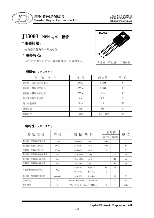
Jingdao Electronic Corporation V01 1/3
Ic (A )集电极电流
Vce(sat )(V )集电极-发射极饱和压降
深圳市晶导电子有限公司 Shenzhen Jingdao Electronic Co.,Ltd.
TEL:0755-29799516 FAX:0755-29799515
静态输出特性 0.5
50mA 0.4
40mA
0.3
30mA
0.2
20mA
10mA 0.1
Ib=0
0
2
4
6
8
10
Vce(V)集电极-发射极电压
Vce(sat)集电极 - 发射极饱和压降- Ic 集电极电流 3
2 Ic=2Ib
1
0.1
0 0.2 0.4
0.6
0.8
IC=0
VCE=5V;
IC=0.2A
VCE=5V;
IC=1mA
IC=0.5A; IB=0.2A
IC=1A;IB1=IB2=0.2A;VCE=300V
VCE=10V;IC=0.1A;f =1MHz
规范值
最小值 最大值
400
700
9
20
10
10
15
35
8
0.6
0.3
8
单位
V V V uA uA uA
V uS MHz
25mA 0.4
20mA
0.3
15mA
0.2
10mA
5mA 0.1
Ib=0
0
2
4
68Leabharlann 10Vce(V)集电极-发射极电压
Vce(sat)集电极 - 发射极饱和压降- Ic 集电极电流 3
C33-07 Standard Specification for Concrete Aggregates

1
C 33 – 07
Ground Blast-Furnace Slag in Preventing Excessive Expansion of Concrete Due to the Alkali-Silica Reaction C 535 Test Method for Resistance to Degradation of LargeSize Coarse Aggregate by Abrasion and Impact in the Los Angeles Machine C 586 Test Method for Potential Alkali Reactivity of Carbonate Rocks as Concrete Aggregates (Rock-Cylinder Method) C 595 Specification for Blended Hydraulic Cements C 618 Specification for Coal Fly Ash and Raw or Calcined Natural Pozzolan for Use in Concrete C 637 Specification for Aggregates for Radiation-Shielding Concrete C 638 Descriptive Nomenclature of Constituents of Aggregates for Radiation-Shielding Concrete C 666/C 666M Test Method for Resistance of Concrete to Rapid Freezing and Thawing C 989 Specification for Ground Granulated Blast-Furnace Slag for Use in Concrete and Mortars C 1105 Test Method for Length Change of Concrete Due to Alkali-Carbonate Rock Reaction C 1157 Performance Specification for Hydraulic Cement C 1240 Specification for Silica Fume Used in Cementitious Mixtures C 1260 Test Method for Potential Alkali Reactivity of Aggregates (Mortar-Bar Method) C 1293 Test Method for Determination of Length Change of Concrete Due to Alkali-Silica Reaction C 1567 Test Method for Determining the Potential AlkaliSilica Reactivity of Combinations of Cementitious Materials and Aggregate (Accelerated Mortar-Bar Method) D 75 Practice for Sampling Aggregates D 3665 Practice for Random Sampling of Construction Materials E 11 Specification for Wire Cloth and Sieves for Testing Purposes
2SJ103_07中文资料

4
2007-11-01
Absolute Maximum Ratings (Ta = 25°C)
Characteristics
Symbol
Rating
UnitΒιβλιοθήκη Gate-drain voltage Gate current Drain power dissipation Junction temperature Storage temperature range
2SJ103
3
2007-11-01
元器件交易网
2SJ103
RESTRICTIONS ON PRODUCT USE
• The information contained herein is subject to change without notice.
20070701-EN GENERAL
JEDEC
TO-92
temperature, etc.) may cause this product to decrease in the
JEITA
SC-43
reliability significantly even if the operating conditions (i.e. operating temperature/current/voltage, etc.) are within the
TOSHIBA
2-5F1C
absolute maximum ratings. Please design the appropriate reliability upon reviewing the
Weight: 0.21 g (typ.)
Toshiba Semiconductor Reliability Handbook (“Handling
- 1、下载文档前请自行甄别文档内容的完整性,平台不提供额外的编辑、内容补充、找答案等附加服务。
- 2、"仅部分预览"的文档,不可在线预览部分如存在完整性等问题,可反馈申请退款(可完整预览的文档不适用该条件!)。
- 3、如文档侵犯您的权益,请联系客服反馈,我们会尽快为您处理(人工客服工作时间:9:00-18:30)。
TO-92TO-126PRODUCT SUMMARYBV CEO 400V BV CBO 700V I C1.5AV CE(SAT)0.8V @ I C / I B = 0.5A / 0.1AFeatures● High Voltage● High Speed SwitchingStructure● Silicon Triple Diffused Type ● NPN Silicon TransistorOrdering InformationPart No.PackagePackingTS13003CT B0 TO-92 1Kpcs / Bulk TS13003CT B0G TO-92 1Kpcs / Bulk TS13003CT A3 TO-92 2Kpcs / Ammo TS13003CT A3G TO-92 2Kpcs / Ammo TS13003CK B0TO-1261Kpcs / BulkNote: “G” denote for Sb FreeBlock DiagramAbsolute Maximum Rating (Ta = 25o C unless otherwise noted)ParameterSymbolLimitUnitCollector-Base Voltage V CBO 700V V Collector-Emitter Voltage V CEO 400V V Emitter-Base Voltage V EBO9 V DC 1.5 Collector CurrentPulse I C 3 A TO-92 1.5 Total Power Dissipation @ Tc= 25oC TO-126P tot 30 WOperating Junction TemperatureT J +150 o C Operating Junction and Storage Temperature RangeT STG- 55 to +150oCThermal PerformanceParameterSymbolLimitUnitTO-92 122 Junction to Ambient Thermal ResistanceTO-126R ӨJA90oC/WPin Definition: 1. Emitter 2. Collector 3. BasePin Definition:1. Emitter2. Collector3. BaseElectrical Specifications (Ta = 25o C unless otherwise noted)ParameterConditions Symbol Min Typ Max UnitStaticCollector-Base VoltageI C = 1mA, I B = 0 BV CBO 700 -- -- V Collector-Emitter Breakdown Voltage I C = 10mA, I E = 0 BV CEO 400 -- -- V Emitter-Base Breakdown Voltage I E = 1mA, I C = 0 BV EBO 9 -- -- V Collector Cutoff Current V CB = 700V, I E = 0 I CBO -- -- 1 uA Emitter Cutoff CurrentV EB = 9V, I C = 0 I EBO -- -- 1 uACollector-Emitter Saturation Voltage *I C / I B = 0.5A / 0.1A I C / I B = 1.0A / 0.25A I C / I B = 1.5A / 0.5AV CE(SAT)1 V CE(SAT)2 V CE(SAT)3 -- -- -- 0.25 0.5 1.2 0.5 1 3 V Base-Emitter Saturation Voltage *I C / I B = 0.5A / 0.1A I C / I B = 1.0A / 0.25A V BE(SAT)1 V BE(SAT)2-- -- -- -- 1 1.2 V DC Current Gain *V CE = 5V, I C = 10mAV CE = 10V, I C = 400mA V CE = 2V, I C = 1Ah FE6 20 8-- -- --40 40 40Dynamic Characteristics FrequencyV CE = 10V, I C = 0.1A f T 4 -- -- MHz Output Capacitance V CB = 10V, f = 0.1MHz Cob -- 21 -- pF Resistive Load Switching Time (Ratings)Delay Time t d -- 0.05 0.2 uS Rise Time t r -- 0.5 1 uS Storage Time t STG -- 2 4 uS Fall TimeV CC = 125V, I C = 1A, I B1 = I B2 = 0.2A, t p = 25uS Duty Cycle ≤1%t f--0.40.7uS* Note: pulse test: pulse width ≤300uS, duty cycle ≤2%Electrical Characteristics Curve (Ta = 25o C, unless otherwise noted)Figure 1. Static CharacteristicsFigure 2. DC Current GainFigure 3. V CE(SAT) v.s. V BE(SATFigure 4. Power DeratingFigure 5. Reverse Bias SOAFigure 6. Safety Operating AreaTO-92 Mechanical DrawingMarking DiagramY = Year Code M = Month Code(A =Jan, B =Feb, C =Mar, D =Apl, E =May, F =Jun, G =Jul, H =Aug, I =Sep, J =Oct, K =Nov, L =Dec) L = Lot CodeTO-92 DIMENSION MILLIMETERS INCHES DIM MIN MAX MIN MAX A 4.30 4.70 0.169 0.185 B 4.30 4.70 0.169 0.185 C 14.30(typ) 0.563(typ) D 0.43 0.49 0.017 0.019 E 2.19 2.81 0.086 0.111 F 3.30 3.70 0.130 0.146 G 2.42 2.66 0.095 0.105 H0.37 0.43 0.015 0.017TO-126 Mechanical DrawingMarking DiagramY = Year CodeM = Month Code(A =Jan, B =Feb, C =Mar, D =Apl, E =May, F =Jun, G =Jul, H =Aug, I =Sep, J =Oct, K =Nov, L =Dec) L = Lot CodeTO-126 DIMENSION MILLIMETERS INCHES DIM MIN MAX MIN MAX∝1 -- 3ºC --3ºC ∝2 -- 3ºC -- 3ºC ∝3 -- 3ºC -- 3ºC ∝4 -- 3ºC --3ºC A 0.150 0.153 3.81 3.91 B 0.275 0.279 6.99 7.09 C 0.531 0.610 13.50 15.50 D 0.285 0.303 7.52 7.72 E 0.034 0.041 0.95 1.05 F 0.028 0.031 0.71 0.81 G 0.048 0.052 1.22 1.32 H 0.170 0.189 4.34 4.80 I 0.095 0.105 2.41 2.66 J 0.045 0.055 1.14 1.39 K 0.045 0.055 1.14 1.39 L -- 0.021 -- 0.55 M0.137 0.152 3.50 3.86NoticeSpecifications of the products displayed herein are subject to change without notice. TSC or anyone on its behalf, assumes no responsibility or liability for any errors or inaccuracies.Information contained herein is intended to provide a product description only. No license, express or implied, to any intellectual property rights is granted by this document. Except as provided in TSC’s terms and conditions of sale for such products, TSC assumes no liability whatsoever, and disclaims any express or implied warranty, relating to sale and/or use of TSC products including liability or warranties relating to fitness for a particular purpose, merchantability, or infringement of any patent, copyright, or other intellectual property right.The products shown herein are not designed for use in medical, life-saving, or life-sustaining applications. Customers using or selling these products for use in such applications do so at their own risk and agree to fully indemnify TSC for any damages resulting from such improper use or sale.。