spe10396
633938型CATV MATV RG6#18无电导膜双文件+90%铝绕线+PVC外套系列商品说明书

633938 008U1000 Gray UnReel
1,000 ft 612825176077
633938 877500 Natural Reel
500 ft 612825176121
633938 8771000 Natural Reel
1,000 ft 612825176114
633938 877U1000 Natural UnReel
UL Temperature Operating
75°C
0°C to +75°C
Bend Radius Installation Min. 2.3 in Max. Pull Tension: Bulk Cable Weight:
76 lbs (34 kg) 27 lbs/1000ft
Standards and Compliance
Indoor - Plenum, Indoor CA Prop 65, Product Lens™, Environmental Product Declaration (EPD) Available NFPA 262, FT6 CATVP, CMP CMP EU CE Mark, EU Directive 2015/863/EU (RoHS 2 amendment), REACH, EU Directive 2011/65/EU (RoHS 2), EU Directive 2012/19/EU (WEEE) China RoHS II (GB/T 26572-2011)
Overall Cable Diameter (Nominal): 0.233 in (5.92 mm)
Electrical Characteristics
Attenuation
Richtek RT9116 10W Class-D Stereo Speaker Driver A
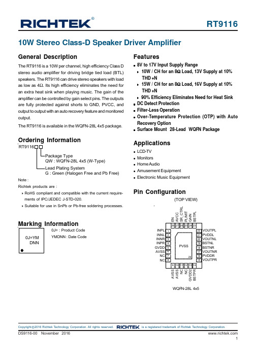
RT9116®©Copyright 2016 Richtek Technology Corporation. All rights reserved. is a registered trademark of Richtek Technology Corporation.Ordering InformationNote :Richtek products are :❝ RoHS compliant and compatible with the current require-ments of IPC/JEDEC J-STD-020.❝ Suitable for use in SnPb or Pb-free soldering processes.Pin Configuration(TOP VIEW)WQFN-28L 4x510W Stereo Class-D Speaker Driver AmplifierGeneral DescriptionThe RT9116 is a 10W per channel, high efficiency Class D stereo audio amplifier for driving bridge tied load (BTL)speakers. The RT9116 can drive stereo speakers with load as low as 4Ω. Its high efficiency eliminates the need for an extra heat sink when playing music. The gain of the amplifier can be controlled by gain select pins. The outputs are fully protected against shorts to GND, PVCC, and output to output with an auto recovery feature and monitored output.The RT9116 is available in the WQFN-28L 4x5 package.Features●8V to 17V Input Supply Range❝ 10W / CH for an 8Ω Load, 13V Supply at 10%THD +N❝ 15W / CH for an 8Ω Load, 16V Supply at 10%THD +N❝ 90% Efficiency Eliminates Need for Heat Sink ●DC Detect Protection ●Filter-Less Operation●Over-Temperature Protection (OTP) with Auto Recovery Option●Surface Mount 28-Lead WQFN PackageApplications●LCD-TV ●Monitors ●Home Audio●Amusement Equipment●Electronic Music EquipmentG : Green (Halogen Free and Pb Free)0J= : Product CodeYMDNN : Date CodeBSTNL PVDDR VOUTNR BSTNR VOUTPRVOUTPL VOUTNL PVDDL L I M I T S T P LA I N N R _C T R L V C C N CB S T P RG V D D 2A V S SN C A V S SRT9116©Copyright 2016 Richtek Technology Corporation. All rights reserved. is a registered trademark of Richtek Technology Corporation.Typical Application CircuitNote :RT9116Copyright 2016 Richtek Technology Corporation. All rights reserved. is a registered trademark of Richtek Technology Corporation.RT9116©Copyright 2016 Richtek Technology Corporation. All rights reserved. is a registered trademark of Richtek Technology Corporation.Functional Block DiagramOUTPLOUTNL OUTPROUTNRBSTPLBSTNLBSTPR BSTNRPVDDL PVDDR AVSS PVSSOperationThe RT9116 is a dual-channel 2 x 10W efficient, Class D audio power amplifier for driving bridge-tied stereo speakers. The RT9116 uses the three-level modulation (BD model) scheme that allows operation without external LC reconstruction when the amplifier is driving an inductive load.Moreover, the built-in spread spectrum modulation can efficiently reduce EMI and save the cost of the external inductor, replaced by ferrite beads.A closed-loop modulator, which enables negative error feedback, can improve THD+N and PSRR of output signals.The RT9116 offers two selectable power limit thresholds,5W/10W under 8Ω for protecting load speakers.These two limit thresholds can be set easily by connecting two different resistors, 25k Ω/150k Ω, from the PLIMIT pin to ground.Though there is no requirement for power limit, theresistance connected from the PLIMIT pin to ground must be greater than 500k Ω.The RT9116 features over-current protection against output stage short-circuit conditions.When a short-circuit condition occurs, amplifier outputs will be switched to a Hi-Z state, and the short-circuit protection latch will be triggered. Once the short-circuit condition is removed, the RT9116 will be automatically recovered.The RT9116 can drive stereo speakers as low as 4Ω. The high efficiency of the RT9116, 90%, eliminates the need for an external heat sink when playing music.RT9116©Copyright 2016 Richtek Technology Corporation. All rights reserved. is a registered trademark of Richtek Technology Corporation.Electrical CharacteristicsAbsolute Maximum Ratings (Note 1)●Supply Voltage, PVDDL, PVDDR, AVCC ----------------------------------------------------------------- −0.3V to 21V●Input Voltage, EN, GAIN -------------------------------------------------------------------------------------- −0.3V to (PVDDx + 0.3V)●Output Voltage, OUTPL,OUTPR,OUTNL,OUTNR ------------------------------------------------------- −0.3V to (PVDDx + 0.3V)●Bootstrap Voltage, BSTPL,BSTPR,BSTNL,BSTNR ----------------------------------------------------−0.3V to (PVDDx + 6V)●Other Pins--------------------------------------------------------------------------------------------------------−0.3V to (GVDD + 0.3V)●Power Dissipation, P D @ T A = 25°CWQFN-28L 4x5------------------------------------------------------------------------------------------------- 3.64W ●Package Thermal Resistance (Note 2)WQFN-28L 4x5, θJA -------------------------------------------------------------------------------------------- 27.4°C/W WQFN-28L 4x5, θJC ------------------------------------------------------------------------------------------- 2°C/W ●Lead Temperature (Soldering, 10 sec.)-------------------------------------------------------------------- 260°C ●Junction T emperature ------------------------------------------------------------------------------------------ 150°C●Storage T emperature Range --------------------------------------------------------------------------------- −65°C to 150°C ●ESD Susceptibility (Note 3)HBM (Human Body Model)----------------------------------------------------------------------------------- 2kVRecommended Operating Conditions (Note 4)●Supply Input Voltage, PVDDL, PVDDR, AVCC ---------------------------------------------------------- 8V to 17V ●Min. SPK load in BTL mode, Rspk (BTL)---------------------------------------------------------------- 4Ω●Junction T emperature Range --------------------------------------------------------------------------------- −40°C to 125°C ●Ambient T emperature Range --------------------------------------------------------------------------------- −40°C to 85°CRT9116©Copyright 2016 Richtek Technology Corporation. All rights reserved. is a registered trademark of Richtek Technology Corporation.Note 1. Stresses beyond those listed “Absolute Maximum Ratings ” may cause permanent damage to the device. These arestress ratings only, and functional operation of the device at these or any other conditions beyond those indicated in the operational sections of the specifications is not implied. Exposure to absolute maximum rating conditions may affect device reliability.Note 2. θJA is measured under natural convection (still air) at T A = 25°C with the component mounted on a high effective-thermal-conductivity four-layer test board on a JEDEC 51-7 thermal measurement standard. θJC is measured at the exposed pad of the package.Note 3. Devices are ESD sensitive. Handling precaution is recommended.Note 4. The device is not guaranteed to function outside its operating conditions.RT9116©Copyright 2016 Richtek Technology Corporation. All rights reserved. is a registered trademark of Richtek Technology Corporation.Output Power vs. Supply Voltage0.02.55.07.510.012.515.017.520.022.525.067891011121314151617181920Supply Voltage (V)O u t p u t P o w e r (W )Efficiency vs. Output Power0102030405060708090100012345678910Output Power (W)E f f i c i e n c y (%)Typical Operating CharacteristicsPVCC = 12V, R L = 8Ω, Gain = 26dBPVCC = 12V, RL = 8Ω, Gain = 26dB1kHz 20Hz 10kHz0.5W 2.5W 5WFrequency (Hz)0-10-20-30-40-50-60-70-80-90-100PVCC = 12V, R L = 8Ω, Gain = 26dB, Po = 1WC r o s s t a l k (d B )20 50 100 200 500 1k 2k 5k 10k 20k R to L L to RFrequency (Hz)40383634323028262422201816141210PVCC = 12V, R L = 8Ω, Gain = 26dB, Po = 1Wd B V (d B )20 50 100 200 500 1k 2k 5k 10k 20kRT9116©Copyright 2016 Richtek Technology Corporation. All rights reserved. is a registered trademark of Richtek Technology Corporation.Application InformationGVDD SupplyThe GVDD is used to supply the Gate Drivers for the output full bridge transistors. Connect a 1μF capacitor from this pin to ground for good bypass. The typical GVDD output voltage is 5V.Amplifier Gain SettingThe gain of the RT9116 amplifier can be set by one input terminals, GAIN shown as Table 1.The gain setting is realized by changing the taps on the input resistors and feedback resistors inside the amplifier.This causes the input impedance (ZI) to be dependent on the gain setting. The actual gain settings are controlled by the ratios of the resistors, so the gain variation from part-to-part is small. However, the input impedance from part-to-part at the same gain may shift by ±20% due to shifts in the actual resistance of the input resistors.Table 1. Gain SettingEN OperationThe RT9116 employs a shutdown mode operation designed to reduce supply current (ICC) to the absolute minimum level for power saving. The EN input terminal should be held high (see specification table for trip point) in normal operation. Pulling EN low causes the outputs to mute and the amplifier to enter a low current state. Leaving EN floating will cause the amplifier operation to be unpredictable. Never leave EN pin unconnected. For the best power-off pop performance, turn off the amplifier in the shutdown mode prior to removing the power supply voltage.Over-Current Protection (OCP)The RT9116 provides OCP function to prevent the device from damages during overload or short-circuit conditions.The current are detected by an internal sensing circuit.Once overload happens, the OCP function is designed to operate in auto-recovery mode.DC Detect ProtectionRT9116 has circuitry which will protect the speakers from DC current which might occur due to defective capacitors on the input or shorts on the printed circuit board at the inputs. To clear the DC Detect it is necessary to cycle the PVCC supply.ADC Detect Fault is issued when the output differential duty-cycle of either channel exceeds 18% (for example,+59%, −41%) for more than 290 msec at the same polarity.This feature protects the speaker from large DC currents or AC currents less than 4Hz. To avoid nuisance faultsdue to the DC detect circuit, hold the SD pin low at power-up until the signals at the inputs are stable. Also, take care to match the impedance seen at the positive andnegative inputs to avoid nuisance DC detect faults.Under-Voltage Protection (UVP)The RT9116 monitors the voltage on PVDD voltage threshold. When the voltage on PVDDL and PVDDR pin falls below the under voltage threshold, 7V (typ.), the UVP circuit turns off the output immediately and operates in cycle by cycle auto-recovery mode.Over-Voltage Protection (OVP)The RT9116 monitors the voltage on PVDD voltage threshold. When the voltage on PVDDL and PVDDR pin rise behind the over voltage threshold, 15V (typ.), the OVP circuit turns off the output immediately and operates in cycle by cycle auto-recovery mode.Over-Temperature Protection (OTP)The OTP prevents damage to the device when the internal die temperature exceeds 170°C. There is a ±15°C tolerance on this trip point from device to device. Once the die temperature exceeds the OTP threshold, the device entersRT9116©Copyright 2016 Richtek Technology Corporation. All rights reserved. is a registered trademark of Richtek Technology Corporation.into the shutdown state and the outputs are disabled. This is not a latched fault. The thermal fault is cleared once the temperature of the die is reduced by 15°C. The device begins normal operation at this point with no external system interaction.Power-On/Off SequenceUse the following sequence to power on the device❝PVCC power supply ready.Past EN = 1 (EN pin goes high)Figure 1. Power On SequenceFigure 2. Power Off SequenceUse the following sequence to power off the device ❝EN = 0 (EN pin goes Low) Past PVCC power supply shutdownThermal ConsiderationsThe junction temperature should never exceed the absolute maximum junction temperature T J(MAX), listed under Absolute Maximum Ratings, to avoid permanent damage to the device. The maximum allowable power dissipation depends on the thermal resistance of the IC package, the PCB layout, the rate of surrounding airflow,and the difference between the junction and ambient temperatures. The maximum power dissipation can be calculated using the following formula :P D(MAX) = (T J(MAX) − T A ) / θJAwhere T J(MAX) is the maximum junction temperature, T A is the ambient temperature, and θJA is the junction-to-ambient thermal resistance.For continuous operation, the maximum operating junction temperature indicated under Recommended Operating Conditions is 125°C. The junction-to-ambient thermal resistance, θJA , is highly package dependent. For a WQFN-28L 4x5 package, the thermal resistance, θJA , is 27.4°C/W on a standard JEDEC 51-7 high effective-thermal-conductivity four-layer test board. The maximum power dissipation at T A = 25°C can be calculated as below :P D(MAX) = (125°C − 25°C) / (27.4°C/W) = 3.64W for a WQFN-28L 4x5 package.The maximum power dissipation depends on the operating ambient temperature for the fixed T J(MAX) and the thermal resistance, θJA . The derating curves in Figur e 3 allows the designer to see the effect of rising ambient temperature on the maximum power dissipation.Power LimitThe voltage at the PLIMIT pin can used to limit the power to levels below that which is possible based on the supply rail. Add a resistor (Table 2) to ground set the voltage at the PLIMIT pin. Also add a 1μF capacitor from the PLIMIT pin to ground. The PLIMIT circuit sets a limit on the output Power.PVCCENPVCCENFigure 3. Derating Curve of Maximum Power Dissipation0.00.40.81.21.62.02.42.83.23.64.0255075100125Ambient Temperature (°C)M a x i m u m P o w e r D i s s i p a t i o n (W )RT9116©Copyright 2016 Richtek Technology Corporation. All rights reserved. is a registered trademark of Richtek Technology Corporation.Figure 4. PCB Layout GuideLayout ConsiderationsFor the best performance of the RT9116, the below PCB layout guidelines must be strictly followed.Place the decoupling capacitors as close as possible to the AVCC, PVDDL, PVDDR and GND pins. For achieving a good quality, consider adding a small, good performance low ESR ceramic capacitor between 220pF and 1000pF and a larger mid-frequency capacitor between 0.1μF and 1μF to the PVDD pins of the chip. The traces of (LINP &LINN, RINP & RINN) and (OUTPL & OUTNL, OUTPR &OUTNR) should be kept equal width and length respectively. The thermal pad must be soldered to the PCB for proper thermal performance and optimal reliability.The dimensions of the thermal pad and thermal land should be larger for application. The vias should connect to a solid copper plane, either on an internal layer or on the bottom layer of the PCB.Audio InputNote : The configuration of the Pin #1 identifier is optional,W-Type 28L QFN 4x5 PackageRichtek Technology Corporation14F, No. 8, Tai Yuen 1st Street, Chupei CityHsinchu, Taiwan, R.O.C.Tel: (8863)5526789Richtek products are sold by description only. Richtek reserves the right to change the circuitry and/or specifications without notice at any time. Customers should obtain the latest relevant information and data sheets before placing orders and should verify that such information is current and complete. Richtek cannot assume responsibility for use of any circuitry other than circuitry entirely embodied in a Richtek product. Information furnished by Richtek is believed to be accurate and reliable. However, no responsibility is assumed by Richtek or its subsidiaries for its use; nor for any infringements of patents or other rights of third parties which may result from its use. No license is granted by implication or otherwise under any patent or patent rights of Richtek or its subsidiaries.DS9116-00 November 11。
LT3496EUFD 1 三路降压LED驱动器说明书
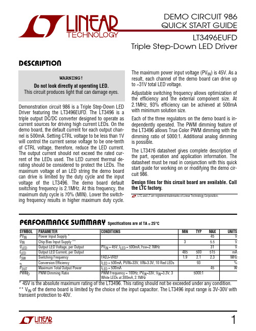
LT3496EUFD DESCRIPTIONWARNING!Do not look directly at operating LED. This circuit produces light that can damage eyes.Demonstration circuit 986 is a Triple Step-Dow n LED Driver f eaturing the LT3496EUFD. The LT3496 is a triple output DC/DC converter designed to operate as current sources f or driving high current LEDs. On the demo board, the def ault current f or each output chan-nel is 500mA. Setting CTRL voltage to be less than 1V w ill control the current sense voltage to be one-tenth of CTRL voltage, theref ore, reduce the LED current. The output current should not exceed the rated cur-rent of the LEDs used. The LED current thermal de-rating should be considered to protect the LEDs. The maximum voltage of an LED string the demo board can drive is limited by the duty cycle and the input voltage of the LT3496. The demo board def ault sw itching f requency is 2.1M Hz. At this f requency, the maximum duty cycle is 70% (M IN). Low er the sw itch-ing f requency results in higher maximum duty cycle.The maximum pow er input voltage (PV IN ) is 45V. As aresult, each channel of the demo board can drive up to ~31V total LED voltage.Adj ustable sw itching f requency allow s optimization of the ef f iciency and the external component size. At 2.1M Hz, 93% ef f iciency can be achieved at 500mA w ith minimum solution size.Each of the three regulators on the demo board is in-dependently operated. The PWM dimming f eature of the LT3496 allow s True Color PWM dimming w ith the dimming ratio of 5000:1. Additional analog dimming is possible.The LT3476 datasheet gives complete description of the part, operation and application inf ormation. The datasheet must be read in conj unction w ith this quick start guide f or w orking on or modif ying the demo cir-cuit 986.Design f iles f or this circuit board are available. Call the LTC f actory., LTC and LT are registered trademarks of Linear Technology Corporation.PERF ORM A NCE SU M M A RY Specif ications are at TA = 25°CSYM BOL PARAM ETERCONDI TI ONSM I N TYP M AXUNI TSPV IN Pow er Input Supply *45 V V IN Chip Bias Input Supply **3 5.5 V V LED Output LED Voltage, per Output PV IN = 45V, I LED = 500mA, Fsw =2.1M Hz 31 V I LED Output LED Current, per Output485 500 515 mA F SWSw itching Frequency FADJ=VREF1.92.1 2.3 M Hz ηConversion Ef f iciencyI LED = 500mA, PVIN=33V, VIN=3.3V, 10 Red LEDs 93 %P OUT M aximum Total Output Pow er I LED = 500mA45 WPWM DPWM Dimming RatioPWM Frequency = 100Hz , PV IN =33V, V IN =3.3V, 3 White LEDs at 300mA, 2.1M Hz5000:1* 45V is the absolute maximum rating of the LT3496. This rating should not be exceeded under any condition. ** V IN of the demo board is limited by the choice of the input capacitor. The LT3496 input range is 3V-30V w ith transient protection to 40V.DEMO CIRCUIT 986Q UICK S TA RT G UIDEL T3496EUF DTrip le S te p -Do w n L ED Driv e rLT3496EUFDQ U ICK STA RT PROCEDU REDemonstration circuit 986 is easy to set up to evaluate the perf ormance of the LT3496EUFD. Ref er to Figure 1 f or proper measurement equipment setup and f ollow the procedure below:1.With pow er of f, connect an input pow er supply to V IN and GND. To achieve highest ef f iciency, a low voltage supply, such as 3.3V or 5V, is recom-mended.2.With pow er of f, connect a second input pow er sup-ply to PV IN and GND. The PV IN absolute maximum rating is 45V.3.If an output channel n is not used, the PWM n should be tied to GND.4.With pow er of f, connect as LED string to an output channel interested. Connect the anode of the f irstLED to the LED n+. Connect the cathode of the last LED to the LED n-. All three channels can operate simultaneously or individually.5.Turn on PV IN pow er supply.6.Turn on V IN pow er supply.7.Check f or the proper LED current and LED string voltage.NOTE.If there is no output, turn of f the pow er supplies. Check allconnections.8.Once the proper output current/voltage are estab-lished, adj ust the parameters w ithin the operating range and observe the output current regulation, ef-f iciency and other parameters.9.To observe PWM dimming, turn of f all pow er sup-plies. Connect the PWM n to a pulse generator. Then repeat step 5 – 8.LT3496EUFDFigure 1.Proper M easurem ent Equipm ent SetupLT3496EUFD。
tef6686的使用手册
tef6686的使用手册tef6686的使用手册一、简介1.1 tef6686概述tef6686是一款高性能、多功能的无线收音机芯片,广泛应用于汽车、家庭音响和便携式收音机等产品中。
该芯片具备强大的接收能力和先进的解调技术,能够接收并播放AM、FM、SW和DAB/DAB+等多种广播频段的节目。
1.2 产品特点- 高接收灵敏度和低噪声特性,保证了音频质量的高保真度。
- 内置多种解调方式,可适应不同频段和编码方式的广播信号。
- 支持数字音频输出,可与其他音频系统进行连接。
- 集成了人机交互接口,操作简单方便。
- 具备数据接口,可与其他外部设备进行数据交互。
1.3 规格参数- 接收频率范围:AM 520-1710kHz,FM 87-108MHz,SW 4.75-21.85MHz,DAB/DAB+ 174-240MHz。
- 输入电压:3.3V。
- 电源消耗:低于100mA。
- 输出音频功率:2.5W。
二、使用方法2.1 连接电源将tef6686芯片与电源进行连接,确保输入电压为3.3V,并控制电源消耗低于100mA。
2.2 调节接收频率根据需要选择收听的频段,如AM、FM、SW或DAB/DAB+,利用人机交互接口或数据接口对接收频率进行调节。
2.3 解调广播信号根据收听的广播频段选择对应的解调方式,如AM、FM、SW或DAB/DAB+,通过tef6686芯片的解调功能进行解码。
2.4 连接音频输出将tef6686芯片的音频输出与其他音频系统进行连接,如功放、扬声器或耳机,以实现音频播放。
2.5 扩展功能根据需要,通过数据接口与其他外部设备进行交互,如调节音量、选择节目、保存频道等功能。
三、观点和理解tef6686作为一款优秀的无线收音机芯片,具备广泛的应用前景。
它的高接收灵敏度和低噪声特性,能够保证音频质量的高保真度,使得用户可以享受到高品质的音乐和广播节目。
tef6686支持多种解调方式,可以适应不同频段和编码方式的广播信号,大大提高了收听的灵活性和多样性。
e96数字代码与英文字母混合标准法
e96数字代码与英文字母混合标准法一、概述e96数字代码与英文字母混合标准法是一种用于表达电阻和电容值的标准表示方法。
它包括三个部分:第一个部分是一个大写字母 "E",代表指数;第二个部分是一个两位的数字代码,代表数量级;第三个部分是一个大写字母 "R" 或 "C",分别代表电阻和电容。
这种表示方法具有一定的规范性和通用性,能够满足不同行业对电阻和电容值表示的需求。
二、e96数字代码部分e96数字代码部分由两位数字组成,分别表示数量级。
它包括了96个数值,范围从10^0到10^2。
这种编码方式能够满足不同精度要求的电阻和电容值的表示。
当需要表示一个100欧姆的电阻时,可以用数字代码50来表示,10^2即表示100欧姆。
同样,当需要表示一个0.1微法的电容时,可以用数字代码50来表示,10^-1即表示0.1微法。
三、英文字母部分英文字母部分分为 "R" 和 "C" 两种,分别代表电阻和电容。
这种表示方法简洁明了,能够清晰地表示器件的类型和特性。
在实际应用中,电子工程师和电路设计师常常使用这种表示方法来标注电子元器件的数值。
四、数字代码与字母混合表示示例以电阻为例,当需要表示一个47千欧姆的电阻时,可以用数字代码66和字母 "R" 来表示,即为66R。
同样,当需要表示一个0.022微法的电容时,可以用数字代码22和字母 "C" 来表示,即为22C。
五、e96数字代码与英文字母混合标准法的优势1. 规范性: e96数字代码与英文字母混合标准法具有一定的规范性,能够满足不同行业对电阻和电容值表示的需求。
2. 通用性: 这种表示方法在全球范围内得到广泛应用,能够满足不同国家和地区对电子元器件数值表示的要求。
3. 简洁明了: 这种表示方法简洁明了,能够清晰地表示器件的类型和特性。
cre6559sf规格书
cre6559sf规格书全文共四篇示例,供读者参考第一篇示例:CRE6559SF规格书是一种用于汽车制造和改装的产品规范文档,它包含了该产品的所有技术要求、功能描述、性能参数等详细信息。
本文将对CRE6559SF规格书进行详细的介绍和解读。
一、产品名称CRE6559SF是一款用于汽车电子系统的集成芯片,主要用于车载娱乐、导航、通信等功能。
二、产品参数1. 尺寸:10mm*10mm*1mm2. 工作电压:3.3V3. 工作频率:1GHz4. 接口:SPI、I2C5. 温度范围:-40℃~85℃6. 存储空间:128MB7. 芯片材质:硅8. 包装形式:BGA封装三、主要功能1. 视频解码:支持多种视频格式的解码,包括MPEG4、H.264等。
2. 音频解码:支持多种音频格式的解码,包括MP3、AAC等。
3. 蓝牙通讯:支持蓝牙通讯功能,可与手机、耳机等设备进行无线通讯。
4. GPS导航:支持GPS导航功能,可以实现车辆的定位、导航等功能。
5. USB接口:支持USB接口,可以接入U盘、移动硬盘等外部设备。
6. 触摸屏控制:支持触摸屏控制功能,可以实现手指操作、手势识别等。
四、性能参数1. 工作稳定性:长时间稳定运行,无死机现象。
2. 响应速度:快速响应用户操作,流畅无卡顿。
3. 通信距离:蓝牙通讯距离达到10米。
4. 定位准确性:GPS导航定位准确性小于5米。
5. 视频播放质量:支持1080P高清视频播放。
五、其他特性1. 低功耗设计:低功耗设计,节能环保。
2. 抗干扰能力:具有很强的抗干扰能力,不受外界干扰。
3. 易于集成:设计紧凑,易于集成到汽车电子系统中。
4. 抗震抗震:具有良好的抗震抗震性能,适用于汽车行驶环境。
第二篇示例:CRE6559SF规格书一、产品概述CRE6559SF是一款全新的智能家居设备,旨在提供更便捷、更智能的生活体验。
它采用最先进的人工智能技术和网络连接技术,能够实现智能控制、远程控制和语音控制等功能,为用户带来更加便捷、舒适的居家生活。
TEF收音芯片选型
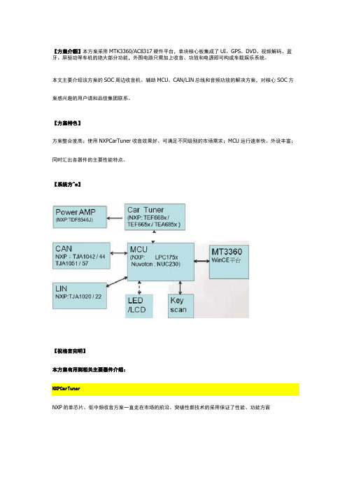
【方案介貂】本方案采用MTK3360/AC8317硬件平台,单块核心板集成了UI、GPS、DVD、视频解码、蓝牙、屏驱动等车机的绝大部分功能,外围电路只需加上收音、功放和电源即可构成车载娱乐系统。
本文主要介绍该方案的SOC周边收音机、辅助MCU、CAN/LIN总线和音频功放的解决方案,对核心SOC方案感兴趣的用户请和品佳集团联系。
【方案特色】方案整合度高;使用NXPCarTuner收音效果好、可满足不同级别的市场需求;MCU运行速率快、外设丰富;同时汇出各器件的主要性能特点。
【系统方^m】【祝格言完明】本方案有用到相关主要器件介绍:NXP的单芯片、低中频收音方案一直走在市场的前沿。
突破性新技术的采用保证了性能、功能方面iCccrn&olurd的领先,集成度不断提高使得开发变得更为简单,PCB 空间逐步减小,整体成本也在不断降低。
如TEF668x 、TEF665x 、TEA685x 三系列收音芯片管脚兼容,性能从高到低全面覆盖,可使产品形成高中低搭配,方便客户的选择。
下面分别介绍:1.NXPTEF668x(Lithio)系歹UTEF668x 低中频调谐器高性能单芯片是单芯片无线电IC ,包括AM/FM 无线电调谐器和软件定义的无线电信号处理。
它们扩展了恩智浦半导体广泛的、行业成熟的汽车无线电单调谐器产品组合,提供出色的无线电性能、最广泛的功能和最先进的软件算法,同时优化了系统成本。
HVQFN 封装占用最小的PCB 空间,并适用于双层和多层PCB 。
无线电接收器包括最高功能集、AM/FM 前端、调谐合成器、信道过滤、FM 信道均衡、FM 多路改善、解调、FM 立体声解码、弱信号处理、噪声抑制和RDS ,并提供与DARC 解调器/解码器的接口。
功能框图:□CO DlYidersFM&PFFM tronLendTEF6G8XAM BFF AM froniendRadto ProM&singAudie □ACDig..!alrMn ^efface12sMp 证I^OuEputbufferbuff&rXTAL3sdllatorDigitalTuRiitgSYstemADC功能特点:•包含调谐器和软件定义无线电处理的免校准数字接收器•基于命令的高级用户接口,兼具高度控制灵活性和易控性。
ALPS小型瞬时型按动开关SPEJ系列选型手册
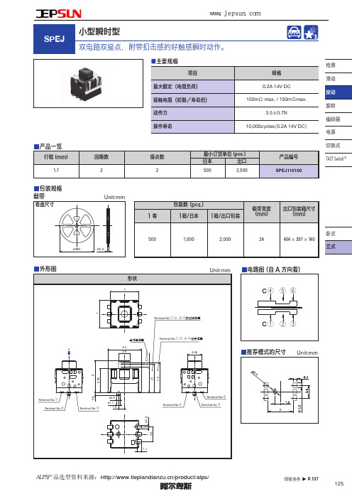
产品一览
行程 (mm) 1.7
回路数 2
接点数 2
最小订货单位 (pcs.)
日本
出口
500
2,000
产品编号 SPEJ110100
检测 滑动 按动 旋转 编码器 电源 切换式 TACT SwitchTM
包装规格 载带
卷盘尺寸
Unit:mm
包装数 (pcs.)
载带宽度 出口包装箱尺寸
1卷
1箱/日本 1箱/出口包装
■浸焊方式的参考举例 适用于 For PC board 端子型
系列
SPPJ3 SPUN SPUJ, SPUP, SPPH2, SPPH4 SPPJ2, SPPH1, SPED2, SPED4, SPEF
预热温度 100℃ max.
项目 预热温度时间 60s max.
100℃ max.
60s max.
操作部 强度
工作 方向
拉引 方向
50N
30N
—
5N for 1minute 50N
50N
0.5N for 1minute
100MΩ 100MΩ min.
max.
100V DC
49N
50N
—
—
—
耐环 境性能
耐寒性能 耐热性能 耐湿性能
–40±2℃ for 96h
–20±2℃ for 96h 85±2℃ for 96h 40±2℃, 90 to 95%RH for 96h
———
———
焊接温度 260±5℃ 260±5℃ 260±5℃ 260±5℃
浸焊 焊接浸渍时间 5±1s 10±1s 5±1s 10±1s
ALPS产品选型资料来源:/product/alps/ 137
- 1、下载文档前请自行甄别文档内容的完整性,平台不提供额外的编辑、内容补充、找答案等附加服务。
- 2、"仅部分预览"的文档,不可在线预览部分如存在完整性等问题,可反馈申请退款(可完整预览的文档不适用该条件!)。
- 3、如文档侵犯您的权益,请联系客服反馈,我们会尽快为您处理(人工客服工作时间:9:00-18:30)。
2010BEHAVIOR OF AL-ZN-IN ANODES AT ELEVATED TEMPERATUREGRANT GIBSONGIBSON APPLIED TECHNOLOGY AND ENGINEERING, LLC16360 PARK TEN PLACE, STE 206 HOUSTON TX 77084gtgibson@ABSTRACT There has been little theoretical and experimental data on the behavior of Al-Zn-In anodes in elevatedtemperature seawater. The majority of the work was aimed at giving the cathodic protection engineer somedirection on the performance of anodes in harsh environments without discussion of the theoretical aspects ofaluminum activation and failure at elevated temperatures. A discussion of previous research is reviewed withrespect to aluminum anode performance in seawater at elevated temperatures. Experiments were conducted ona commercially available aluminum anode at 20, 40, 60, and 80 C in 3.5% NaCl. Current capacity, corrosionmorphology, and hydrogen evolution results are presented and a discussion on anode activation mechanisms isreviewed in relation to the results. This paper focuses on aluminum zinc indium activated anodes.ANODE CHEMISTRY DEVELOPMENTAs a sacrificial anode, aluminum is a very highly favored metal because it possesses a thermodynamicpotential of –1.663V SHE, a high electrochemical equivalent, low density, and a high theoretical current capacity(2980 A ⋅hr/kg). In addition, aluminum is not a precious metal making it economically feasible to use as asacrificial anode. The drawback of aluminum is that its theoretical driving potential is not realized. Aluminumadopts a potential of –700mV SCE in seawater due to the formation of a protective oxide layer 1. This potential isnot active enough to polarize steel to its protection potential. Another drawback is aluminum corrodes by pitting ina seawater environment. While most of the current produced by pitting may well be used in protection of astructure, the anode may become perforated and may lose aluminum by mechanical detachment. Thus, thecurrent capacity of the anode would be diminished.The first aluminum anodes used were binary alloys of aluminum-zinc 2,3,4 and aluminium-tin 4,5. Doremus andDavis 4 give the nominal composition of an Al-Zn alloy as: Zn, 5.0 to 6.0 weight percent; Fe, 0.17% max; Cu,0.02% max; Si, 0.10% max; and Al, remainder. It was claimed to have a capacity of 1540 to 1598 A ⋅hr/kg and anoperating potential of –1.00V Ag/AgCl. The Al-Zn anode was comparable to zinc and was commonly used as areplacement for zinc when weight considerations were paramount. Hine and Wei 5 reported an Al-Sn anode withan operating potential of -1.30V SCE, but upon coupling to a structure, the anode would become polarized tounacceptable levels. It was later found that Al-Sn anodes depended strongly on composition of material and heattreatment. With close manufacturing control, Al-Sn anodes with current capacities of 1050 A ⋅hr/kg and operatingpotentials of –1.1 to –1.2V SCE were realized. Even though these aluminum alloys gave a slight advantage overzinc, they were not readily accepted in the field because of the lack of published data on their performance.Then in 1966, Newport and Reding 6 reported the results of tests on 2500 alloys investigating the effects ofalloying aluminum with many different elements. They found that alloying with Cu and Mn resulted in a potentialmore noble than unalloyed aluminum. Zn, Cd, Mg, and Ba shifted the potential of aluminum negative direction by©2010 by NACE International. Requests for permission to publish this manuscript in any form, in part or in whole, must be in writing to NACEInternational, Publications Division, 1440 South Creek Drive, Houston, Texas 77084. The material presented and the views expressed in this paper are solely those of the author(s) and are not necessarily endorsed by the Association.Paper No.10396100 to 300mV and Ga, Hg, Sn, and In shifted the potential by 300 to 900mV. They found that thedepassivators, or activators, had some common features. The elements had low melting points, a low solubility inAl (except Zn and Mg), and most activating elements did not form intermetallic compounds with Al. Currentefficiency tests showed that none of the binary alloys possessed suitable efficiencies, but it was found that ternaryalloy compositions could greatly enhance the efficiency. Ternary alloy trials resulted in an Al-Zn-Hg alloy that had an operating potential of –1.05V SCE, a current capacity of around 2800 A⋅hr/kg, and a uniform corrosion pattern. They also stressed the control of the purity of the aluminum stock used to produce the alloys. Lowering the purityfrom 99.9% to 99.7% resulted in a loss of 25% in efficiency, but little change in operating potential. Schrieber andReding9 confirmed the laboratory results in field testing in seawater for up to 660 days.In the same month, Sakano, Toda, and Hanada7 reported on a Al-Zn-In sacrificial anode. They also stressedthe importance of purity in the aluminum stock noticing a difference in current capacity by switching from 99.99%purity to 99.85% purity. The best results for a viable anode were obtained with 99.85% purity with 0.025% In,2.52% Zn, and 0.01% Cd. The cadmium was added to soften the corrosion product and improve the corrosioncharacteristics. They do not give the preliminary results showing the effects of different alloy compositions.Since 1966, three ternary alloys have evolved namely tin8, mercury6,9, and indium7,10,11,12,13,14,15 which are allalloyed with zinc. The tin based alloys are no longer preferred because they require very accurate compositions,heat treatments, their parameters vary heavily with current density, suffer non-uniform corrosion, and adherentcorrosion products16. While mercury anodes out-perform both tin and indium anodes, they are no longer usedbecause mercury is hazardous to the environment17,18. Indium based anodes are now the preferred materialbecause they are non-hazardous, experience uniform dissolution, and are easy to manufacture.Most recently, Umay et al19 investigated the interrelation between zinc and indium in aluminum anodes.Anodes with a compositional range of zinc between 1.5% and 5.5% and indium between 0.01% and 0.04% werecast using 99.75% pure aluminum. The impurity content was 0.1% iron, 0.07% silicon, and 0.0005% copper.Figure 1 depicts the anode efficiency as a function of indium and zinc content. The graphs show that at eachzinc content there is an indium content that produces a maximum efficiency. The 1.5, 3.5, and 5.5% zinccompositions with various indium contents produce optimized efficiencies that are local and highly dependent onindium concentration. The 4.5% zinc composition with indium concentrations of 0.017% and 0.026% producesmore of a plateau at an efficiency of 82%. In terms of dissolution morphology, at low indium contents, pits werelocalized, narrow, and deep. At intermediate indium concentrations, the pits were homogeneously distributed andshallow with a smooth pit bottom. At the higher indium concentrations, pit distribution was homogeneous and pitstructure was shallow with deep intergranular corrosion at pit bottoms. The compositional limits are near those ofthe commercial anodes marketed today20, but with slight differences. The difference in anode performance by Umay et al and present commercial anodes can be attributed to the impurity of the stock material.The realization of high performance anodes depends highly on the purity of the aluminum stock with indiumand zinc being the main alloy addition. Much work has been directed in the past two decades to find smalladditions to the stock to counter the deleterious effects of using lower purity aluminum, which would reducemanufacturing costs.Iron and copper are the two most detrimental impurities. They act as residual flaws on the surface of theanode. Also, copper and iron are cathodic to the aluminum matrix and have high exchange current densities forthe electrolytic evolution of hydrogen21. A selection of some of the elements found in aluminum is given in Table 1. The potentials of some of the intermetallics formed in the aluminum matrix are given in Table 222.Table 1. Exchange Current for hydrogen evolution21.Element -Logi o,HIron 5.6Copper 7.8Aluminium 8.0 Zinc 10.5Indium 11.3Mercury 12.3It is those impurities with lower hydrogen overvoltages than aluminum and more noble potentials that hamper the current capacity. Zinc and mercury both have higher hydrogen overvoltages than aluminum although mercury is cathodic to aluminum it is not detrimental. Iron and copper have low hydrogen overvoltages and are highly cathodic to the aluminum matrix. It can be envisioned that as lower purity aluminum stock is used, an increase in cathodic residual flaws is present, and more current is wasted due to hydrogen evolution on the surface of impurities rather than going towards protecting the structure.Table 2. Potential of intermetallics and elements in a NaCl-H2O2 Solution22.Intermetallic Potential (V) Vs. 0.1N CalomelCu -0.11Si -0.17CuAl2 -0.44FeAl3 -0.47FeMnAl12 -0.75 Al (high purity) -0.76Zn -1.26 The effects of copper, iron, and silicon on the current capacity of an Al-Zn-Sn anode developed by Ponchel and Horst8 are shown in Figure 2. As shown, copper has by far the most detrimental effect at weight percentages as low as 0.01%. Iron can be tolerated up to concentrations of around 0.1%. Silicon has a more gradual effect and can be tolerated at higher concentrations. It was also mentioned that nickel has an effect similar to copper on the current capacity. The work was done on Al-Zn-Sn anodes and the data may be subject to many errors as mentioned earlier16. The aim was to show the effects and importance of individual impurities at very low levels. Hence, it is not surprising that Ponchel and Horst8 set strict controls on the purity of aluminum stock: Fe, 0.1% max.; Si, 0.1% max; Cu, 0.009% max.In contrast, Sakano et al7 (Al-Zn-In) found that iron is beneficial for the current capacity up to a certain level. Exceeding this level would result in a loss in capacity. Copper was found to be very detrimental at a concentration of 0.019%. They also point out copper affects the corrosion characteristics, causing pitting and adherence of corrosion products. In regards to silicon, they found that it decreased the efficiency to 86% from around 92%. Silicon had the harmful effects of lowering the anode potential, irregular corrosion patterns, and lengthy induction periods (time for anode to reach operating potential). With the above observations, Sakano et al set their impurity limits as Fe, 0.1% max; Si, ~0.04%; Cu, <0.02%.R. F. May12 investigated the beneficial effects of iron in high performance Al-Zn-In anodes. More uniform corrosion was observed when specific additions of iron were made to high purity stock. This effect was offset by a loss in efficiency. May argues that using a higher purity stock drives up the cost of anode and also reduces the anode activation pattern. From Table 2, adding small amounts of manganese would alloy with the iron to produce intermetallics that would be near the potential of the matrix, thus reducing the local cell action effects of the iron. May suggests that the iron intermetallic phases, or residual flaws, promote initial dissolution. He coins the term “activation initiators.” May concludes that by adding manganese to the alloy, higher iron levels can be tolerated, and uniformity of anode attack can be maintained. A specific alloy composition was not given, but May does mention European Patent 018712723. It specifies a maximum effect with a manganese weight percent between 0.01% and 0.20%.Zamin24 studied Al-Mn binary alloys and the effect of iron concentration on corrosion resistance. He found that Mn increases the corrosion resistance of Al and increasing the Mn concentration can alleviate the detrimental effect of iron. He found that the presence of Mn alone has no effect but depends solely on the Mn/Fe ratio. Work by Klinghoffer and Linder25 showed that a ratio of 1:1 was the most beneficial. Balancing the Mn/Fe ratio, they were able to produce an Al-Zn-In (Zn, 4.0%; In, 0.24%) anode with up to 0.20% Fe. A summary of their work is shown in Figure 3. The current capacity increases up to a ratio of 1:1 and then decreases dramatically. The operating potential is not affected until a ratio of 1:1 is exceeded where it becomes more noble.Googan26 studied aluminum and aluminium-1.0% Zn with iron additions between 0.05% and 1.0%. The work found that iron is mostly segregated as a grain boundary intermetallic phase FeAl3. He proposes the “Iron-Dissolution-Electrodeposition” process in which dissolution of FeAl3 results in ferrous ions depositing to form a layer of pure iron on the alloy surface. The pure iron deposit stimulates the cathodic reaction kinetics, which results in increased local cell action and ultimately a loss in efficiency. Seeking a solution to the problem, Googan found the 0.5% germanium overcomes the deleterious effects of the iron. In contrast to manganese, the germanium does not alter the FeAl3 intermetallic but instead interferes with the deposition of the ferrous ions. The phenomenon would then inhibit the production of low hydrogen overvoltage iron deposits.In 1978, Smith, Reding, and Riley10 developed commercially available anode1 consisting of Al-Zn-In-Si. They did not report on the iron or copper contents but did state that the silicon sequesters the iron to form an intermetallic that is less cathodic than pure iron or silicon. The silicon works in the same way as manganese in that it is the ratio of silicon to iron which is important. Presently, Al-Zn-In alloys can be produced with up to 0.5% iron with 85% efficiency17.1 Galvalum IIIKobayashi and Tamura15 reported the results of tests of various alloy additions. Figure 4 shows the effect of silicon on the operating potential and current capacity of Al-Zn-In alloy2 which has an iron impurity concentration of 0.14%. The silicon ranges between 0.07% and 0.4%. A maximum appears in the current capacity at about 0.15% silicon. It can be concluded that the optimum situation is an iron-silicon ratio of 1:1, which is close to that of the manganese.BEHAVIOR OF ANODES AT ELEVATED TEMPERATUREAt present there has been little theoretical investigation into the behavior of aluminum based anodes in elevated temperature seawater. The majority of the work was aimed at giving the cathodic protection engineer some direction on the performance of aluminum based anodes in harsh environments. The main environment studied was seabed mud. Elevated temperature seawater tests are few and far between and their results are rarely discussed. A review and an in-depth study of indium activated anodes in mud has been completed by Erricker27 and will not be discussed here. This section presents results of indium activated anodes in elevated temperature seawater and brine.Murai, Tamura, and Miura28,29 studied a Al-Zn-Sn-Bi-Ga alloy in seawater from 0 to 80°C at 3 and 10 A/m2 for 240 hours. The anode potential remained constant at –1.080V SCE from 10 to 50°C at 3 A/m2. At 10 A/m2, the anode polarized to –1.055V SCE and remained constant from 20°C till around 60°C. The potential became more noble above 60°C reaching approximately -1.020V SCE at 80°C, with not much difference between 3 and 10 A/m2. They attribute the change in potential at higher temperature to the growth of boehmite. The current efficiency was 95% between 0 and 40°C. At 70°C, the current efficiency is 88% for 3 A/m2 and 91% for 10 A/m2. When the seawater temperature was increased to 80°C, the current efficiency decreased rapidly to 40% for 3 A/m2 and 51% for 10 A/m2. The corrosion pattern was identical over the temperature range 0 to 60°C showing general attack. Above 70°C, the corrosion pattern was more localized. They do not discuss any possible explanation for the rapid loss in efficiency above 70°C.Smith, Reding, and Riley10 tested an Al-Zn-In-Si alloy in 75°C 15% brine. At a current density of 2.1 A/m2, the alloy delivered 2000 A⋅h/kg and an operating potential of –1060 mV SCE. The same alloy delivered 2500 A⋅h/kg and –1080 mV SCE in full seawater tests. Additional studies in low salinity seawater showed that the operating potential of the alloy became more positive as the salinity decreased. This indicates that the potential of the alloy might be related to resistivity of the environment much like the breakdown potential is on the chloride activity. No change in current capacity was noted with change in salinity.Schrieber and Murray30,31 report the results of 30 day tests on Al-Zn-In-Si and Al-Zn-Hg anodes at 38, 66, and 93°C using current densities of 2.2 A/m2 and 6.5 A/m2 in 3 and 7% NaCl. In general, the anode potential became more noble with increasing temperature. Increasing the brine concentration lowered the operating potential. At 2.2 A/m2, the current capacity increases slightly with increasing temperature from 38 to 66°C, whilst the current capacity is relatively unchanged for the higher current density over this temperature range. In agreement with Murai et al28,29, the current capacity decreases rapidly above a temperature near 70°C. The data for 2.2 A/m2 is summarized in Figure 5. The corrosion morphology was uniform for both alloys at 38 and 66°C. In line with the decrease in current capacity at 93°C, the morphology was uneven and localized. Schrieber and Murray do not discuss possible mechanisms for the behavior of the anodes with increasing temperature.Kobayashi and Tamura32 reported similar results on an Al-Zn-In alloy. They conducted their tests in artificial seawater between 5 and 100°C at 10 A/m2 for 240 hours. The current capacity for the alloy was approximately 2620 A⋅h/kg between 5 and 65°C. Above 80°C, the current capacity decreased to about 1000 A⋅h/kg at 100°C. The operating potential of the alloy was –1.10V SCE until 50°C. Above 50°C, the operating potential increases to –1.00V SCE at 100°C. They state that the growth of boehmite may cause the operating potential to become more noble. Corrosion morphology change with temperature was not discussed.Wroe and May33,12 only reported results for 5 and 95°C. At the elevated temperature, Al-Zn-In alloy gave a current capacity of 474 A⋅h/kg and an operating potential of –1.074V SCE. They claim that a high magnesium, low manganese alloy delivers 1125 A⋅h/kg and –1.05V SCE at 95°C. These results are compared against those2 Alanode IIIat 5°C which gave values of –1.120V SCE and 2634 A⋅h/kg for the Al-Zn-In and –1.130V SCE and 2794 A⋅h/kg for the high Mg low Mn alloy.Fischer34 studied the effects of temperature and depth on the behavior of Al-Zn-In anodes in natural seawater. Current densities from 0.5 to 5 A/m2 and pressures from 1 to 50 bar were used in a 60 day test. In agreement with previous cited work, the operating potential of the anode increased with increasing temperature. The current capacity was largely dependent on the current density and temperature. At 0.5 A/m2, increasing the temperature from 10°C to 70°C increased the current capacity from about 2000 A⋅h/kg to around 2200 A⋅h/kg. At 5 A/m2, increasing the temperature from 10°C to 70°C gradually decreased the current capacity from about 2080 A⋅h/kg to 1400 A⋅h/kg. The results at 0.5 A/m2 are in agreement with Schrieber and Murray30,31 , being that the current capacity increased with temperature for low current densities. Fischer did not test above 70°C. At ambient temperature and pressure, Fischer observed an even distribution of pits over the anode surface. At higher temperatures, the corrosion morphology was much more irregular with deep large pits and grooves. In general, at higher temperature, the corrosion morphology was more localized and increasing the pressure further localized the attack.At present, not much work has been directed to the mechanism behind the behavior of aluminum-based anodes at higher temperatures. From the above discussion, some observations need to be addressed. First, the operating potential becomes more noble with increasing temperature. Second, the current capacity either increases with increasing temperature for low current densities or decreases with temperature if the current density is above some value. Third, the corrosion morphology changes from uniform to very localized with increasing temperature.EXPERIMENTAL WORKSacrificial anode parameters form the core of cathodic protection design. The two most important electrochemical parameters are the operating potential and the current capacity. Other factors are the corrosion morphology, long term output characteristics, and anode structure. Short-term electrochemical tests are used to measure the electrochemical properties of anode material, but the most accurate test is a long term field test35. The problems with long-term tests are the time to complete the test and the ability to obtain reproducible results. Thus, anode producers have a vested interest in short term testing of sacrificial anodes.The most popular of the various tests is the galvanostatic test which involves the passage of a constant current through the anode test specimen for a specified time whilst measuring its potential. The current capacity is calculated by the weight loss of the sample and the total amount of charge passed (A⋅h). The weight loss method measures the sum of all the sources of inefficiency. A different approach for measuring efficiency using the galvanostatic test is to measure the volume of hydrogen evolved from the sample over a known period of time.Both current capacity tests were performed on the anode material alloy C3 and alloy X at room and elevated temperatures. Two types of alloys were tested: alloy C (commercially available chemistry) and for comparative purposes alloy X (non-commercial alloy – made for scientific research). The nominal composition of the alloys is given in Table 3. Alloy X is nominally the same as alloy C but with a lower composition in indium. It was aimed that in comparing the two alloys some insight into the activation mechanism of indium would be gained.The alloys were received as sticks and samples were machined using a band saw and finished to the desired height with a lathe. After the samples were cut, preparation was performed as follows. First, the samples were scrubbed using a nylon brush with soap and water. Afterwards, the samples were cleaned with acetone and a nylon brush. Finally, the samples were dried in an oven for 15 minutes at 120°C.A general schematic diagram of the weight loss galvanostatic test is shown in Figure 6. The main components are the test sample, electrolyte bath, cathode, coulometer, and galvanostat.All tests were performed in 15 liters of de-ionized water with 3.5% NaCl. The NACE36 and DNV37 prescribe using artificial seawater or circulated real full strength seawater. Due to the amount of tests and volume of electrolyte needed, this was deemed uneconomical. The solution was at room temperature which varied between 17 and 22ºC. The tests performed at room temperature are designated as 20ºC.3 Alloys were provided by Impalloy Alloys Ltd. Alloy C is a generic name for a commercially available alloy Impalloy III. Alloy X is a generic name for an alloy specially cast for experimental purposes and is not commercially available.Table 3. Nominal compositions of alloys (weight percent). Element Alloy C Alloy XZinc 4.67 4.91 Indium 0.0175 0.0039Iron 0.083 0.047Silicon 0.86 0.049Copper 0.0024 0.0007Gallium 0.0082 0.0121Titanium 0.0198 0.0239Aluminum Balance BalanceExperimental Procedure15 liters of electrolyte per tank were prepared the day before the test was to begin. On the following day, the pH was set to 8.2 by addition of HCl or NaOH. Next, the samples and copper plating rod were weighed. The samples were placed in the centre of the cathodes, which were placed in the centre of the tanks. The sample level was centered between the bottom of the tank and the electrolyte level. With all the components of the test connected in series, the current was set with the galvanostat as to give the desired current density. The potential of the anode was measured with a saturated calomel electrode (SCE) connected to a saturated KCl agar-agar Luggin probe and a high impedance digital voltmeter. The SCE reference electrode remained at room temperature for all tests. From the start of the test, the potential was measured at 1,3,24, 96, and 168 hours. When the test was complete (168 hours), the galvanostat was turned off and the samples were removed from the electrolyte. They were cleaned using distilled water and a nylon brush, rinsed in acetone, and dried at 120°C for 15 minutes. The copper plating rod was rinsed with distilled water, then acetone, and also dried at 120°C for 15 minutes. The copper plating rod and the samples were re-weighed and the current capacity was calculated by the following formula:)( )( 8433.0)/( grams Sample of Loss Weight grams Rod Copper Gain Weight kg h A Capacity Current ⋅=⋅ The samples were finally categorized and stored in plastic bags for later examination.Elevated Temperature Tests - ExperimentalFigure 7 shows the internal components of the heat jacket, the top cover, and a photograph of the heat jacket and temperature controller. The internal container for the electrolyte was a carbon steel cylinder of 15.5cm inner diameter, 25.5cm depth, and wall thickness of 0.5cm. 4 liters of 3.5% NaCl electrolyte was used. Surrounding the steel cylinder was galvanized steel mesh and aluminum foil. Heater tape was formed around the mesh and foil and itself fully enclosed by a layer of aluminum foil. The next layer was a covering of fiberglass cloth wrap followed by a layer of pink housing fiberglass insulation. Lastly, steel mesh was wrapped around to maintain shape. The exterior was covered by packaging tape to prevent contact with the fiberglass and for aesthetic reasons.The top was machined from a polypropylene sheet of 2.5cm thickness and diameter of 17.7cm. A lip was also machined to the inner diameter of the steel cylinder to insure a snug fit. The centre of the top was bored to a diameter of 4.5cm. Three other holes (1.1cm diameter) were drilled and tapped for cable glands. The centre bore allowed installation and removal of the sample from the experimental kit. The three cable glands allowed a thermometer and a Luggin probe to be fitted and the third was a spare.The temperature was controlled by a capillary thermostat. The thermostat is operated from a remote bulb connected by a 1m capillary. The temperature range for the thermostat was 0 to 120°C. The thermostat, indicator light, and connections to heater tape were installed in a housing fitted with a 3-amp fuse. The final product is shown in Figure 7.The procedure for the elevated temperature experiments are the same as for the room temperature experiments including duration of test. The pH of the electrolyte was adjusted to 8.2 before heating. It usually required 3 to 7 hours for the desired temperature to be reached. The samples were immersed in the solution after it reached the desired temperature. The SCE reference electrode remained at room temperature for all tests. This may give rise to a minor thermal liquid junction potential. Ashworth and Fairhurst 38 reported the magnitude to be ≤5mV. The error would be present in all tests and was deemed acceptable. The temperatures studied were 40, 60, and 80°C.Hydrogen Evolution Tests - ExperimentalHydrogen evolution tests were designed to quantify the amount of inefficiency due to local cell action. The efficiencies measured could then be compared to the weight loss experiments with the aim of separating the total efficiency loss into mechanical loss, negative difference effect, and local cell action.Hydrogen evolution experiments at room temperature were performed using the weight loss apparatus described above. An inverted 50mL burette fitted with a funnel was used to collect the hydrogen gas. The samples were started at the desired current density. Hydrogen collection was started 24 hours after the start of the test. The burette and funnel were placed symmetrically over the sample with funnel level with the top of the sample. The electrolyte was drawn into the burette with a pipette filler. Collection time was between 3 to 24 hours depending on the amount of gas collected. The efficiency was calculated by the following formula⎥⎦⎤⎢⎣⎡⋅+=(min))(132 %T mL V Current Applied Current Applied Efficiencywhere V is the change in volume of gas collected over the time period T .For elevated temperatures, the apparatus shown in Figure 8 was used. A 5 litre Quick Fit jar was fitted with steel mesh. A 5-inlet Quick Fit top was used to hold the titanium rod to support the sample, support the burette, and allow electrical connection to the cathode. The whole jar was then submerged into an elevated temperature bath thermistatically controlled to ±2°C. The samples were run for 24 hours prior to gas collection. The temperature of the burette was measured by taping a thermocouple to the burette in the area of gas collection and the constant of 132 was adjusted for the temperature.EXPERIMENTAL RESULTSThis section presents the results of how current density and temperature affect the current capacity, operating potential, and corrosion morphology of alloy C and alloy X. The current capacity was measured by the weight loss and hydrogen evolution methods over the current densities of 0.1 to 6 A/m 2. For comparative purposes, alloy X was tested only at 3 A/m 2 at elevated temperature. The aim was to gain some insight into the mechanism of indium activation, the mechanism of efficiency loss, and assess the feasibility of using a commercially available anode alloy at elevated temperature.Results at 20°CThe operating potential for alloy X versus current density after 7 days exposure is shown in Figure 9. Averaged over all the current densities, alloy X had a mean operating potential of -977±3 mV SCE. One sample was run at a current density of 60 A/m 2 and had an operating potential of -930mV SCE showing that a considerable current density is needed to polarize the alloy.The addition of indium (Impalloy III) decreased the operating potential by over 125mV to -1110±3 mV SCE. The operating potential versus current density after 7 days exposure for alloy C is also shown in Figure 10. Again, the operating potential is independent of the current density measured. In line with alloy X, running alloy C at 60 A/m 2 resulted in polarization of ~43mV to -1070mV SCE.Operating potentials measured in this study agree well with those given in the literature. Doremus and Davis 4 & Hine and Wei 5 reported the potential of an Al-5%Zn alloy to be -780mV SCE. Sakano et al 7 reported a potential of -1100mV SCE for an Al-Zn-In alloy in 1966. Schrieber and Murray 31 measured a value of -1.108mV AgCl Seawater for an Al-Zn-In-Si anode in artificial seawater. This is close to a value of -1090mV SCE reported。