HD74AC02P中文资料
HD74LS02P中文资料

HD74LS02Quadruple 2-Input Positive NOR GatesREJ03D0389–0200Rev.2.00Feb.18.2005 Features• Ordering InformationPart Name Package Type Package Code(Previous Code)PackageAbbreviationTaping Abbreviation(Quantity)HD74LS02P DILP-14pin PRDP0014AB-B(DP-14AV)P —HD74LS02FPEL SOP-14 pin (JEITA) PRSP0014DF-B(FP-14DAV)FP EL (2,000 pcs/reel)HD74LS02RPEL SOP-14 pin (JEDEC) PRSP0014DE-A(FP-14DNV)RP EL (2,500 pcs/reel)Note: Please consult the sales office for the above package availability. Pin ArrangementCircuit Schematic (1/4)Absolute Maximum RatingsUnitRatingsItem SymbolSupply voltage V CC Note 7 VInput voltage V IN 7 V Power dissipation P T 400 mW Storage temperature Tstg –65 to +150 °CNote: Voltage value, unless otherwise noted, are with respect to network ground terminal.Recommended Operating ConditionsUnitMaxItem SymbolMinTypSupply voltage V CC 4.75 5.00 5.25 VI OH — — –400 µAOutput currentI OL — — 8 mA°C7525–20Operating temperature ToprElectrical Characteristics(Ta = –20 to +75 °C)ItemSymbol min. typ.* max. Unit Condition V IH 2.0 — — V Input voltageV IL — — 0.8 V V OH 2.7 — — V V CC = 4.75 V, V IL = 0.8 V, I OH = –400 µA— — 0.5 I OL = 8 mAOutput voltageV OL— — 0.4 V I OL = 4 mAV CC = 4.75 V, V IH = 2 V I IH — — 20 µA V CC = 5.25 V, V I = 2.7 V I IL — — –0.4 mA V CC = 5.25 V, V I = 0.4 VInput current I I — — 0.1 mA V CC = 5.25 V, V I = 7 V Short-circuit outputcurrent I OS –20— –100 mA V CC = 5.25 V I CCH — 1.6 3.2 mA V CC = 5.25 VSupply currentI CCL — 2.8 5.4 mA V CC = 5.25 VInput clamp voltage V IK — — –1.5 V V CC = 4.75 V, I IN = –18 mA Note: * V CC = 5 V, Ta = 25°CSwitching Characteristics(V CC = 5 V, Ta = 25°C)Item Symbol min. typ. max. Unit Conditiont PLH — 10 15 nsPropagation delay time t PHL — 10 15 ns C L = 15 pF, R L = 2 k ΩNote: Refer to Test Circuit and Waveform of the Common Item "TTL Common Matter (Document No.: REJ27D0005-0100)".Package Dimensions RENESAS SALES OFFICESRefer to "/en/network" for the latest and detailed information.Renesas Technology America, Inc.450 Holger Way, San Jose, CA 95134-1368, U.S.ATel: <1> (408) 382-7500, Fax: <1> (408) 382-7501Renesas Technology Europe LimitedDukes Meadow, Millboard Road, Bourne End, Buckinghamshire, SL8 5FH, U.K.Tel: <44> (1628) 585-100, Fax: <44> (1628) 585-900Renesas Technology Hong Kong Ltd.7th Floor, North Tower, World Finance Centre, Harbour City, 1 Canton Road, Tsimshatsui, Kowloon, Hong KongTel: <852> 2265-6688, Fax: <852> 2730-6071Renesas Technology Taiwan Co., Ltd.10th Floor, No.99, Fushing North Road, Taipei, TaiwanTel: <886> (2) 2715-2888, Fax: <886> (2) 2713-2999Renesas Technology (Shanghai) Co., Ltd.Unit2607 Ruijing Building, No.205 Maoming Road (S), Shanghai 200020, ChinaTel: <86> (21) 6472-1001, Fax: <86> (21) 6415-2952Renesas Technology Singapore Pte. Ltd.1 Harbour Front Avenue, #06-10, Keppel Bay Tower, Singapore 098632Tel: <65> 6213-0200, Fax: <65> 6278-8001。
HD74ALVC2G240US资料

Item Propagation delay time Enable time Disable time
•
VCC = 1.5±0.1 V
Symbol tPLH tPHL tZH tZL tHZ tLZ Min 2.0 2.0 2.0 Typ Max 7.0 7.0 7.0 Unit ns ns ns Test conditions CL = 15 pF CL = 15 pF CL = 15 pF FROM (Input) A OE OE TO (Output) Y Y Y
Rev.1, Jan. 2002, page 5 of 13
HD74ALVC2G240
Switching Characteristics
(Ta = −40 to 85°C) • VCC = 1.2 V
Symbol tPLH tPHL tZH tZL tHZ tLZ Min Typ 5.5 6.5 4.5 Max Unit ns ns ns Test conditions CL = 15 pF CL = 15 pF CL = 15 pF FROM (Input) A OE OE TO (Output) Y Y Y
mA mA mA mA mW °C
VI < 0 VO < 0 or VO > VCC VO = 0 to VCC
The absolute maximum ratings are values which must not individually be exceeded, and furthermore, no two of which may be realized at the same time. 1. The input and output voltage ratings may be exceeded if the input and output clamp-current ratings are observed. 2. This value is limited to 4.6 V maximum. 3. The maximum package power dissipation was calculated using a junction temperature of 150°C.
HD74HC09P中文资料

HD74HC09Quad. 2-input AND Gates (with open drain outputs)ADE-205-409 (Z)1st. EditionSep. 2000 Features• High Speed Operation: t pd = 8 ns typ (C L = 50 pF)• High Output Current: Fanout of 10 LSTTL Loads• Wide Operating Voltage: V CC = 2 to 6 V• Low Input Current: 1 µA max• Low Quiescent Supply Current: I CC (static) = 1 µA max (Ta = 25°C)Pin ArrangementHD74HC092DC CharacteristicsTa = 25°CTa = –40 to +85°CItem Symbol V CC (V)Min Typ Max MinMax Unit Test ConditionsInput voltageV IH2.0 1.5—— 1.5—V4.5 3.15—— 3.15—6.04.2—— 4.2—V IL2.0——0.5—0.5V 4.5—— 1.35—1.356.0——1.8— 1.8Output voltageV OL2.0—0.00.1—0.1VVin = V IH or V IL I OL = 20 µA4.5—0.00.1—0.16.0—0.00.1—0.14.5——0.26—0.33I OL = 4 mA 6.0——0.26—0.33I OL = 5.2 mAOff-state output current Io (off) 6.0——±0.5—±5.0µA Vin = V IH or V ILVout = V CC or GND Input current Iin 6.0——±0.1—±1.0µA Vin = V CC or GNDQuiescent supply currentI CC6.0——1.0—10µAVin = V CC or GND, Iout = 0 µAAC Characteristics (C L = 50 pF, Input t r = t f = 6 ns)Ta = 25°CTa = –40 to +85°CItem SymbolV CC (V)Min Typ Max MinMax Unit Test ConditionsPropagation delay t PLH2.0——90—115nstime4.5—1018—236.0——15—20t PHL 2.0——90—115ns 4.5—618—236.0——15—20Output fall timet THL2.0——75—95ns 4.5—515—196.0——13—16Input capacitanceCin——510—10pFHD74HC09 Package Dimensions3HD74HC094HD74HC095Cautions1.Hitachi neither warrants nor grants licenses of any rights of Hitachi’s or any third party’s patent,copyright, trademark, or other intellectual property rights for information contained in this document.Hitachi bears no responsibility for problems that may arise with third party’s rights, includingintellectual property rights, in connection with use of the information contained in this document.2.Products and product specifications may be subject to change without notice. Confirm that you have received the latest product standards or specifications before final design, purchase or use.3.Hitachi makes every attempt to ensure that its products are of high quality and reliability. However,contact Hitachi’s sales office before using the product in an application that demands especially high quality and reliability or where its failure or malfunction may directly threaten human life or cause risk of bodily injury, such as aerospace, aeronautics, nuclear power, combustion control, transportation,traffic, safety equipment or medical equipment for life support.4.Design your application so that the product is used within the ranges guaranteed by Hitachi particularly for maximum rating, operating supply voltage range, heat radiation characteristics, installationconditions and other characteristics. Hitachi bears no responsibility for failure or damage when used beyond the guaranteed ranges. Even within the guaranteed ranges, consider normally foreseeable failure rates or failure modes in semiconductor devices and employ systemic measures such as fail-safes, so that the equipment incorporating Hitachi product does not cause bodily injury, fire or other consequential damage due to operation of the Hitachi product.5.This product is not designed to be radiation resistant.6.No one is permitted to reproduce or duplicate, in any form, the whole or part of this document without written approval from Hitachi.7.Contact Hitachi’s sales office for any questions regarding this document or Hitachi semiconductor products.Hitachi, Ltd.Semiconductor & Integrated Circuits.Nippon Bldg., 2-6-2, Ohte-machi, Chiyoda-ku, Tokyo 100-0004, Japan Tel: Tokyo (03) 3270-2111 Fax: (03) 3270-5109Copyright © Hitachi, Ltd., 2000. All rights reserved. Printed in Japan.Hitachi Asia Ltd. Hitachi Tower16 Collyer Quay #20-00, Singapore 049318Tel : <65>-538-6533/538-8577 Fax : <65>-538-6933/538-3877URL : .sg URLNorthAmerica : /Europe : /hel/ecg Asia : Japan : http://www.hitachi.co.jp/Sicd/indx.htmHitachi Asia Ltd.(Taipei Branch Office)4/F, No. 167, Tun Hwa North Road, Hung-Kuo Building, Taipei (105), Taiwan Tel : <886>-(2)-2718-3666 Fax : <886>-(2)-2718-8180 Telex : 23222 HAS-TPURL : Hitachi Asia (Hong Kong) Ltd. Group III (Electronic Components) 7/F., North Tower, World Finance Centre,Harbour City, Canton Road Tsim Sha Tsui, Kowloon, Hong KongTel : <852>-(2)-735-9218 Fax : <852>-(2)-730-0281URL : Hitachi Europe Ltd.Electronic Components Group.Whitebrook ParkLower Cookham Road MaidenheadBerkshire SL6 8YA, United Kingdom Tel: <44> (1628) 585000Fax: <44> (1628) 585160Hitachi Europe GmbHElectronic Components Group Dornacher Stra βe 3D-85622 Feldkirchen, Munich GermanyTel: <49> (89) 9 9180-0Fax: <49> (89) 9 29 30 00Hitachi Semiconductor (America) Inc.179 East Tasman Drive,San Jose,CA 95134 Tel: <1> (408) 433-1990Fax: <1>(408) 433-0223For further information write to:Colophon 2.0。
HD74HC240P中文资料

HD74HC240Octal Buffers/Line Drivers/Line Receivers(with inverted 3-state outputs)REJ03D0594–0200(Previous ADE-205-471)Rev.2.00Jan 31, 2006 DescriptionThe HD74HC240 is an inverting buffer and has two active low enables (1G and 2G). Each enable independently controls 4 buffers. This device does not have schmitt trigger inputs.Features• High Speed Operation: t pd = 10 ns typ (C L = 50 pF)• High Output Current: Fanout of 15 LSTTL Loads• Wide Operating Voltage: V CC = 2 to 6 V• Low Input Current: 1 µA max• Low Quiescent Supply Current: I CC (static) = 4 µA max (Ta = 25°C)• Ordering InformationPart Name Package TypePackage Code(Previous Code)PackageAbbreviationTaping Abbreviation(Quantity)HD74HC240P DILP-20pin PRDP0020AC-B(DP-20NEV)P —HD74HC240FPEL SOP-20 pin (JEITA) PRSP0020DD-B(FP-20DAV)FP EL (2,000 pcs/reel)HD74HC240RPEL SOP-20 pin (JEDEC) PRSP0020DC-A(FP-20DBV)RP EL (1,000 pcs/reel)HD74HC240TELL TSSOP-20pin PTSP0020JB-A(TTP-20DAV)T ELL (2,000 pcs/reel)Note: Please consult the sales office for the above package availability.Function TableInputs OutputG A YH X ZL H LL L HH : high levelL : low levelX : irrelevantZ : off (high-impedance) state of a 3-state outputPin ArrangementLogic DiagramAbsolute Maximum RatingsItem Symbol Ratings UnitSupply voltage range V CC –0.5 to 7.0 V Input / Output voltage V IN , V OUT –0.5 to V CC +0.5 V Input / Output diode current I IK , I OK ±20 mA Output current I O ±35 mA V CC , GND current I CC or I GND ±75 mA Power dissipation P T 500 mW Storage temperature Tstg –65 to +150 °C Note: The absolute maximum ratings are values, which must not individually be exceeded, and furthermore, no two ofwhich may be realized at the same time.Recommended Operating ConditionsItem Symbol Ratings Unit ConditionsSupply voltage V CC 2 to 6 V Input / Output voltage V IN , V OUT 0 to V CC V Operating temperature Ta –40 to 85 °C 0 to 1000 V CC = 2.0 V0 to 500 V CC = 4.5 V Input rise / fall time *1 t r , t f 0 to 400 ns V CC = 6.0 V Notes: 1. This item guarantees maximum limit when one input switches.Waveform: Refer to test circuit of switching characteristics.Electrical CharacteristicsTa = 25°C Ta = –40 to+85°CItem Symbol V CC (V)Min Typ Max Min MaxUnitTest Conditions2.0 1.5 — — 1.5— 4.5 3.15 — — 3.15 — V IH6.0 4.2 — — 4.2 —V 2.0 — — 0.5 — 0.5 4.5 — — 1.35 — 1.35Input voltageV IL6.0 — — 1.8 — 1.8V 2.0 1.9 2.0 — 1.9 — 4.5 4.4 4.5 — 4.4 — 6.0 5.9 6.0 — 5.9 — I OH = –20 µA 4.5 4.18 — — 4.13 — I OH = –6 mA V OH6.0 5.68 — — 5.63— V Vin = V IH or V IL I OH = –7.8 mA2.0 — 0.0 0.1 —0.1 4.5 — 0.0 0.1 — 0.1 6.0 — 0.0 0.1 — 0.1 I OL = 20 µA 4.5 — — 0.26 — 0.33 I OL = 6 mA Output voltage V OL6.0 — — 0.26 —0.33 V Vin = V IH or V IL I OL = 7.8 mA Off-state output currentI OZ 6.0— — ±0.5 — ±5.0 µA Vin = V IH or V IL ,Vout = V CC or GNDInput current Iin 6.0 — — ±0.1 — ±1.0 µA Vin = V CC or GNDQuiescent supply current I CC 6.0— — 4.0 — 40 µA Vin = V CC or GND, Iout = 0 µASwitching Characteristics(C L = 50 pF, Input t r = t f = 6 ns)Ta = 25°C Ta = –40 to +85°CItem Symbol V CC (V)Min Typ Max Min MaxUnitTest Conditions2.0 — — 90 — 115 4.5 — 10 18 — 23 t PHL6.0 — — 15 — 20 ns 2.0 — — 90 — 115 4.5 — 10 18 — 23 Propagation delaytimet PLH6.0 — — 15 — 20 ns 2.0 — — 150 — 190 4.5 — 11 30 — 38 t ZL6.0 — — 26 — 33 ns 2.0 — — 150 — 190 4.5 — 12 30 — 38 Output enable time t ZH6.0 — — 26 — 33 ns 2.0 — — 150 — 190 4.5 — 16 30 — 38 t LZ6.0 — — 26 — 33 ns 2.0 — — 150 — 190 4.5 — 19 30 — 38 Output disabletimet HZ6.0 — — 26 —33 ns 2.0 — — 60 —75 4.5 — 4 12 — 15 Output rise/fall timet TLH t THL 6.0 — — 10 — 13 ns Input capacitance Cin— — 5 10—10 pFTest CircuitWaveformsPackage Dimensions RENESAS SALES OFFICESRefer to "/en/network" for the latest and detailed information.Renesas Technology America, Inc.450 Holger Way, San Jose, CA 95134-1368, U.S.ATel: <1> (408) 382-7500, Fax: <1> (408) 382-7501Renesas Technology Europe LimitedDukes Meadow, Millboard Road, Bourne End, Buckinghamshire, SL8 5FH, U.K.Tel: <44> (1628) 585-100, Fax: <44> (1628) 585-900Renesas Technology (Shanghai) Co., Ltd.Unit 205, AZIA Center, No.133 Yincheng Rd (n), Pudong District, Shanghai 200120, ChinaTel: <86> (21) 5877-1818, Fax: <86> (21) 6887-7898Renesas Technology Hong Kong Ltd.7th Floor, North Tower, World Finance Centre, Harbour City, 1 Canton Road, Tsimshatsui, Kowloon, Hong KongTel: <852> 2265-6688, Fax: <852> 2730-6071Renesas Technology Taiwan Co., Ltd.10th Floor, No.99, Fushing North Road, Taipei, TaiwanTel: <886> (2) 2715-2888, Fax: <886> (2) 2713-2999Renesas Technology Singapore Pte. Ltd.1 Harbour Front Avenue, #06-10, Keppel Bay Tower, Singapore 098632Tel: <65> 6213-0200, Fax: <65> 6278-8001Renesas Technology Korea Co., Ltd.Kukje Center Bldg. 18th Fl., 191, 2-ka, Hangang-ro, Yongsan-ku, Seoul 140-702, KoreaTel: <82> (2) 796-3115, Fax: <82> (2) 796-2145Renesas Technology Malaysia Sdn. BhdUnit 906, Block B, Menara Amcorp, Amcorp Trade Centre, No.18, Jalan Persiaran Barat, 46050 Petaling Jaya, Selangor Darul Ehsan, MalaysiaTel: <603> 7955-9390, Fax: <603> 7955-9510© 2006. Renesas Technology Corp., All rights reserved. Printed in Japan.。
HD74LS03P中文资料

HD74LS03Quadruple 2-Input Positive NAND Gates(with Open Collector Outputs)REJ03D0390–0200Rev.2.00Feb.18.2005 Features• Ordering InformationPart Name Package Type Package Code(Previous Code)PackageAbbreviationTaping Abbreviation(Quantity)HD74LS03P DILP-14pin PRDP0014AB-B(DP-14AV)P —HD74LS03FPEL SOP-14 pin (JEITA) PRSP0014DF-B(FP-14DAV)FP EL (2,000 pcs/reel)Note: Please consult the sales office for the above package availability. Pin ArrangementCircuit Schematic (1/4)Absolute Maximum RatingsItem Symbol Ratings UnitSupply voltage V CC Note 7 V Input voltage V IN 7 V Power dissipation P T 400 mW Storage temperature Tstg –65 to +150 °C Note: Voltage value, unless otherwise noted, are with respect to network ground terminal.Recommended Operating ConditionsItem Symbol Min Typ Max UnitSupply voltage V CC 4.75 5.00 5.25 V Output voltage V OH — — 5.5 V Output current I OL — — 8 mA Operating temperature Topr –20 25 75 °CElectrical Characteristics(Ta = –20 to +75 °C)ItemSymbol min. typ.* max. UnitConditionV IH 2.0 — — V Input voltage V IL — — 0.8 V — — 0.5I OL = 8 mA Output voltageV OL— — 0.4VI OL = 4 mAV CC = 4.75 V, V IH = 2 VI IH — — 20 µA V CC = 5.25 V, V I = 2.7 VI IL — — –0.4 mA V CC = 5.25 V, V I = 0.4 VInput current I I —— 0.1 mA V CC = 5.25 V, V I = 7 V Output current I OH — — 100 µA V CC = 4.75 V, V IH = 0.8 V, V OH = 5.5 VI CCH — 0.8 1.6 mA V CC = 5.25 VSupply currentI CCL — 2.4 4.4 mA V CC = 5.25 VInput clamp voltage V IK — — –1.5 V V CC = 4.75 V, I IN = –18 mA Note: * V CC = 5 V, Ta = 25°CSwitching Characteristics(V CC = 5 V, Ta = 25°C)Item Symbol min. typ. max. Unit Conditiont PLH — 17 32 nsPropagation delay timet PHL — 25 28 ns C L = 15 pF, R L = 2 k Ω Note: Refer to Test Circuit and Waveform of the Common Item "TTL Common Matter (Document No.: REJ27D0005-0100)".Package Dimensions RENESAS SALES OFFICESRefer to "/en/network" for the latest and detailed information.Renesas Technology America, Inc.450 Holger Way, San Jose, CA 95134-1368, U.S.ATel: <1> (408) 382-7500, Fax: <1> (408) 382-7501Renesas Technology Europe LimitedDukes Meadow, Millboard Road, Bourne End, Buckinghamshire, SL8 5FH, U.K.Tel: <44> (1628) 585-100, Fax: <44> (1628) 585-900Renesas Technology Hong Kong Ltd.7th Floor, North Tower, World Finance Centre, Harbour City, 1 Canton Road, Tsimshatsui, Kowloon, Hong KongTel: <852> 2265-6688, Fax: <852> 2730-6071Renesas Technology Taiwan Co., Ltd.10th Floor, No.99, Fushing North Road, Taipei, TaiwanTel: <886> (2) 2715-2888, Fax: <886> (2) 2713-2999Renesas Technology (Shanghai) Co., Ltd.Unit2607 Ruijing Building, No.205 Maoming Road (S), Shanghai 200020, ChinaTel: <86> (21) 6472-1001, Fax: <86> (21) 6415-2952Renesas Technology Singapore Pte. Ltd.1 Harbour Front Avenue, #06-10, Keppel Bay Tower, Singapore 098632Tel: <65> 6213-0200, Fax: <65> 6278-8001。
HD74LS00PDIP中文资料
元器件交易网Hitachi CodeJEDECEIAJWeight (reference value)DP-14ConformsConforms0.97 gUnit: mm元器件交易网Hitachi CodeJEDECEIAJWeight (reference value)FP-14DA —Conforms 0.23 g*Dimension including the plating thickness Base material dimension° – 8°Hitachi CodeJEDEC EIAJWeight (reference value)FP-14DN Conforms Conforms 0.13 g° – 8°*Pd platingCautions1.Hitachi neither warrants nor grants licenses of any rights of Hitachi’s or any third party’s patent,copyright, trademark, or other intellectual property rights for information contained in this document.Hitachi bears no responsibility for problems that may arise with third party’s rights, includingintellectual property rights, in connection with use of the information contained in this document.2.Products and product specifications may be subject to change without notice. Confirm that you have received the latest product standards or specifications before final design, purchase or use.3.Hitachi makes every attempt to ensure that its products are of high quality and reliability. However,contact Hitachi’s sales office before using the product in an application that demands especially high quality and reliability or where its failure or malfunction may directly threaten human life or cause risk of bodily injury, such as aerospace, aeronautics, nuclear power, combustion control, transportation,traffic, safety equipment or medical equipment for life support.4.Design your application so that the product is used within the ranges guaranteed by Hitachi particularly for maximum rating, operating supply voltage range, heat radiation characteristics, installationconditions and other characteristics. Hitachi bears no responsibility for failure or damage when used beyond the guaranteed ranges. Even within the guaranteed ranges, consider normally foreseeable failure rates or failure modes in semiconductor devices and employ systemic measures such as fail-safes, so that the equipment incorporating Hitachi product does not cause bodily injury, fire or other consequential damage due to operation of the Hitachi product.5.This product is not designed to be radiation resistant.6.No one is permitted to reproduce or duplicate, in any form, the whole or part of this document without written approval from Hitachi.7.Contact Hitachi’s sales office for any questions regarding this document or Hitachi semiconductor products.Hitachi, Ltd.Semiconductor & Integrated Circuits.Nippon Bldg., 2-6-2, Ohte-machi, Chiyoda-ku, Tokyo 100-0004, Japan Tel: Tokyo (03) 3270-2111 Fax: (03) 3270-5109Copyright ' Hitachi, Ltd., 1999. All rights reserved. Printed in Japan.Hitachi Asia Pte. Ltd.16 Collyer Quay #20-00Hitachi TowerSingapore 049318Tel: 535-2100Fax: 535-1533URLNorthAmerica : http:/Europe : /hel/ecg Asia (Singapore): .sg/grp3/sicd/index.htm Asia (Taiwan): /E/Product/SICD_Frame.htm Asia (HongKong): /eng/bo/grp3/index.htm Japan : http://www.hitachi.co.jp/Sicd/indx.htmHitachi Asia Ltd.Taipei Branch Office3F, Hung Kuo Building. No.167, Tun-Hwa North Road, Taipei (105)Tel: <886> (2) 2718-3666Fax: <886> (2) 2718-8180Hitachi Asia (Hong Kong) Ltd.Group III (Electronic Components)7/F., North Tower, World Finance Centre,Harbour City, Canton Road, Tsim Sha Tsui,Kowloon, Hong Kong Tel: <852> (2) 735 9218Fax: <852> (2) 730 0281 Telex: 40815 HITEC HXHitachi Europe Ltd.Electronic Components Group.Whitebrook ParkLower Cookham Road MaidenheadBerkshire SL6 8YA, United Kingdom Tel: <44> (1628) 585000Fax: <44> (1628) 778322Hitachi Europe GmbHElectronic components Group Dornacher Stra§e 3D-85622 Feldkirchen, Munich GermanyTel: <49> (89) 9 9180-0Fax: <49> (89) 9 29 30 00Hitachi Semiconductor (America) Inc.179 East Tasman Drive,San Jose,CA 95134 Tel: <1> (408) 433-1990Fax: <1>(408) 433-0223For further information write to:。
HD74LS00RPEL中文资料

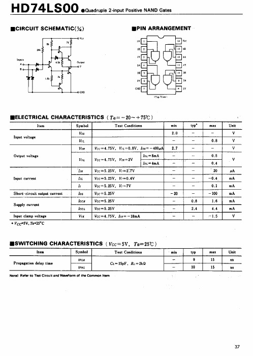
HD74LS00Quadruple 2-Input NAND GatesREJ03D0387–0200Rev.2.00Feb.18.2005 Features• Ordering InformationPart Name Package Type Package Code(Previous Code)PackageAbbreviationTaping Abbreviation(Quantity)HD74LS00P DILP-14pin PRDP0014AB-B(DP-14AV)P —HD74LS00FPEL SOP-14 pin (JEITA) PRSP0014DF-B(FP-14DAV)FP EL (2,000 pcs/reel)HD74LS00RPEL SOP-14 pin (JEDEC) PRSP0014DE-A(FP-14DNV)RP EL (2,500 pcs/reel)Note: Please consult the sales office for the above package availability. Pin ArrangementCircuit Schematic (1/4)Absolute Maximum RatingsUnitRatingsItem SymbolSupply voltage V CC Note 7 VInput voltage V IN 7 V Power dissipation P T 400 mW Storage temperature Tstg –65 to +150 °CNote: Voltage value, unless otherwise noted, are with respect to network ground terminal.Recommended Operating ConditionsUnitMaxItem SymbolMinTypSupply voltage V CC 4.75 5.00 5.25 VI OH — — –400 µAOutput currentI OL — — 8 mA°C7525–20Operating temperature ToprElectrical Characteristics(Ta = –20 to +75 °C)ItemSymbol min. typ.* max. Unit Condition V IH 2.0 — — V Input voltageV IL — — 0.8 V V OH 2.7 — — V V CC = 4.75 V, V IL = 0.8 V, I OH = –400 µA— — 0.5 I OL = 8 mAOutput voltageV OL— — 0.4 V I OL = 4 mAV CC = 4.75 V, V IH = 2 V I IH — — 20 µA V CC = 5.25 V, V I = 2.7 V I IL — — –0.4 mA V CC = 5.25 V, V I = 0.4 VInput current I I — — 0.1 mA V CC = 5.25 V, V I = 7 V Short-circuit outputcurrent I OS –20— –100 mA V CC = 5.25 V I CCH — 0.8 1.6 mA V CC = 5.25 VSupply currentI CCL — 2.4 4.4 mA V CC = 5.25 VInput clamp voltage V IK — — –1.5 V V CC = 4.75 V, I IN = –18 mA Note: * V CC = 5 V, Ta = 25°CSwitching Characteristics(V CC = 5 V, Ta = 25°C)Item Symbol min. typ. max. Unit Conditiont PLH — 9 15 nsPropagation delay time t PHL — 10 15 ns C L = 15 pF, R L = 2 k ΩNote: Refer to Test Circuit and Waveform of the Common Item "TTL Common Matter (Document No.: REJ27D0005-0100)".Package Dimensions RENESAS SALES OFFICESRefer to "/en/network" for the latest and detailed information.Renesas Technology America, Inc.450 Holger Way, San Jose, CA 95134-1368, U.S.ATel: <1> (408) 382-7500, Fax: <1> (408) 382-7501Renesas Technology Europe LimitedDukes Meadow, Millboard Road, Bourne End, Buckinghamshire, SL8 5FH, U.K.Tel: <44> (1628) 585-100, Fax: <44> (1628) 585-900Renesas Technology Hong Kong Ltd.7th Floor, North Tower, World Finance Centre, Harbour City, 1 Canton Road, Tsimshatsui, Kowloon, Hong KongTel: <852> 2265-6688, Fax: <852> 2730-6071Renesas Technology Taiwan Co., Ltd.10th Floor, No.99, Fushing North Road, Taipei, TaiwanTel: <886> (2) 2715-2888, Fax: <886> (2) 2713-2999Renesas Technology (Shanghai) Co., Ltd.Unit2607 Ruijing Building, No.205 Maoming Road (S), Shanghai 200020, ChinaTel: <86> (21) 6472-1001, Fax: <86> (21) 6415-2952Renesas Technology Singapore Pte. Ltd.1 Harbour Front Avenue, #06-10, Keppel Bay Tower, Singapore 098632Tel: <65> 6213-0200, Fax: <65> 6278-8001。
74HC02中文资料_数据手册_参数
INPUT nA, nB
UNIT LOADCOEFFICIENT 1.50
AC CHARACTERISTICS FOR 74HCT GND = 0 V; tr = tf = 6 ns; CL = 50 pF
SYMBOL PARAMETER
tPHL/ tPLH tTHL/ tTLH
min.
propagation delay nA, nB to nY
output transition time
Tamb (°C)
74HCT
+25
−40 to+85
typ. max. min. max.
11 19
24
7 15
19
−40 to+125 min. max.
29 22
UNIT
ns ns
TEST CONDITIONS
VCC WAVEFORMS (V)
4.5 Fig.6 4.5 Fig.6
For the DC characteristics see “74HC/HCT/HCU/HCMOS Logic Family Specifications”.
Output capability: standard ICC category: SSI
AC CHARACTERISTICS FOR 74HC GND = 0 V; tr = tf = 6 ns; CL = 50 pF
Quad 2-input NOR gate
Product specification
74HC/HCT02
DC CHARACTERISTICS FOR 74HCT For the DC characteristics see “74HC/HCT/HCU/HCMOS Logic Family Specifications”. Output capability: standard ICC category: SSI
- 1、下载文档前请自行甄别文档内容的完整性,平台不提供额外的编辑、内容补充、找答案等附加服务。
- 2、"仅部分预览"的文档,不可在线预览部分如存在完整性等问题,可反馈申请退款(可完整预览的文档不适用该条件!)。
- 3、如文档侵犯您的权益,请联系客服反馈,我们会尽快为您处理(人工客服工作时间:9:00-18:30)。
HD74AC02Quad 2-Input NAND GateREJ03D0240–0200Z(Previous ADE-205-356 (Z))Rev.2.00Jul.16.2004Features• Outputs Source/Sink 24 mA • Ordering InformationPart Name Package Type Package Code Package Abbreviation Taping Abbreviation (Quantity)HD74AC02P DIP-14 pinDP-14, -14AV P —HD74AC02FPEL SOP-14 pin (JEITA)FP-14DAV FP EL (2,000 pcs/reel)HD74AC02RPEL SOP-14 pin (JEDEC)FP-14DNV RP EL (2,500 pcs/reel)HD74AC02TELLTSSOP-14 pinTTP-14DVTELL (2,000 pcs/reel)Notes: 1.Please consult the sales office for the above package availability.2.The packages with lead-free pins are distinguished from the conventional products by adding V at the end ofthe package code.Pin ArrangementAbsolute Maximum RatingsItemSymbol RatingsUnit Condition Supply voltageV CC –0.5 to 7V –20mA V I = –0.5V DC input diode current I IK 20mA V I = Vcc+0.5V DC input voltage V I –0.5 to Vcc+0.5V –50mA V O = –0.5V DC output diode current I OK 50mA V O = Vcc+0.5VDC output voltageV O –0.5 to Vcc+0.5V DC output source or sink current I O±50mA DC V CC or ground current per output pin I CC , I GND ±50mA Storage temperatureTstg–65 to +150°CRecommended Operating ConditionsItemSymbol RatingsUnitConditionSupply voltageV CC 2 to 6V Input and output voltage V I , V O 0 to V CC V Operating temperature Ta –40 to +85°C V CC = 3.0V V CC = 4.5 V Input rise and fall time (except Schmitt inputs)V IN 30% to 70% V CCtr, tf8ns/VV CC = 5.5 VDC CharacteristicsTa = 25°C Ta = –40 to +85°C ItemSym-bol Vcc (V)min.typ.max.min.max.UnitCondition3.0 2.1 1.5— 2.1—4.5 3.15 2.25— 3.15—V IH5.53.85 2.75— 3.85—V OUT = 0.1 V or V CC –0.1 V3.0— 1.500.9—0.94.5— 2.25 1.35— 1.35Input Voltage V IL5.5— 2.75 1.65— 1.65VV OUT = 0.1 V or V CC –0.1 V3.0 2.9 2.99— 2.9—4.5 4.4 4.49— 4.4—5.5 5.4 5.49— 5.4—V IN = V IL or V IH I OUT = –50 µA 3.0 2.58—— 2.48—I OH = –12 mA 4.53.94—— 3.80—I OH = –24 mA V OH5.5 4.94—— 4.80—V IN = V IL or V IHI OH = –24 mA3.0—0.0020.1—0.14.5—0.0010.1—0.15.5—0.0010.1—0.1V IN = V IL or V IH I OUT = 50 µA 3.0——0.32—0.37I OL = 12 mA 4.5——0.32—0.37I OL = 24 mA Output voltageV OL5.5——0.32—0.37VV IN = V IL or V IHI OL = 24 mAInput leakage currentI IN 5.5——±0.1—±1.0µA V IN = V CC or GND I OLD 5.5———86—mA V OLD = 1.1 V Dynamic output current *I OHD5.5———–75—mA V OHD = 3.85 V Quiescent supply currentI CC 5.5—— 4.0—40µA V IN = V CC or ground*Maximum test duration 2.0 ms, one output loaded at a time.AC CharacteristicsTa = +25°CCL = 50 pFTa = –40°C to +85°CCL= 50 pFItem Symbol VCC(V)*1Min Typ Max Min Max UnitPropagation delay tPLH3.3 1.0 5.07.5 1.08.0ns5.0 1.0 4.06.0 1.0 6.5Propagation delay tPHL3.3 1.0 5.07.5 1.08.0ns5.0 1.0 4.56.5 1.07.0Note: 1.Voltage Range 3.3 is 3.3 V ± 0.3 VVoltage Range 5.0 is 5.0 V ± 0.5 VCapacitanceItem Symbol Typ Unit ConditionInput capacitance CIN 4.5pF VCC= 5.5 VPower dissipation capacitance CPD 30.0pF VCC= 5.0 VPackage Dimensions RENESAS SALES OFFICESRenesas Technology America, Inc.450 Holger Way, San Jose, CA 95134-1368, U.S.ATel: <1> (408) 382-7500 Fax: <1> (408) 382-7501Renesas Technology Europe Limited.Dukes Meadow, Millboard Road, Bourne End, Buckinghamshire, SL8 5FH, United KingdomTel: <44> (1628) 585 100, Fax: <44> (1628) 585 900Renesas Technology Europe GmbHDornacher Str. 3, D-85622 Feldkirchen, GermanyTel: <49> (89) 380 70 0, Fax: <49> (89) 929 30 11Renesas Technology Hong Kong Ltd.7/F., North Tower, World Finance Centre, Harbour City, Canton Road, Hong KongTel: <852> 2265-6688, Fax: <852> 2375-6836Renesas Technology Taiwan Co., Ltd.FL 10, #99, Fu-Hsing N. Rd., Taipei, TaiwanTel: <886> (2) 2715-2888, Fax: <886> (2) 2713-2999Renesas Technology (Shanghai) Co., Ltd.26/F., Ruijin Building, No.205 Maoming Road (S), Shanghai 200020, ChinaTel: <86> (21) 6472-1001, Fax: <86> (21) 6415-2952Renesas Technology Singapore Pte. Ltd.1, Harbour Front Avenue, #06-10, Keppel Bay Tower, Singapore 098632Tel: <65> 6213-0200, Fax: <65> 6278-8001© 2004. Renesas Technology Corp., All rights reserved. Printed in Japan.Colophon .1.0。