H5N5001FM-E中文资料
05H1中文资料

VOLTAGE RANGE 50 to 600 Volts CURRENT 0.5 AmpereMAXIMUM RATINGS (@ T A =25 O C unless otherwise noted)RATINGSMaximum Recurrent Peak Reverse Voltage Maximum RMS Voltage Maximum DC Blocking VoltageMaximum Average Forward Rectified Current at T A = 55oC Peak Forward Surge Current 8.3 ms single half sine-wave superimposed on rated load (JEDEC method)Typical Junction Capacitance (Note 2)Typical Thermal Resistance (Note 4)Operating and Storage Temperature RangeSYMBOL V RRM V DC I O I FSM C J T J , T STGV RMS Amps 0.5151303015R q JA R q JL -55 to + 150AmpspFCC/W UNITS 50355010070100Volts Volts Volts 1220014020060042060040028040030021030005H105H205H305H405H505H6ELECTRICAL CHARACTERISTICS (At T A = 25o C unless otherwise noted)NOTES : 1. Test Conditions: I F = 0.5A, I R = -1.0A, I RR = -0.25A2. Measured at 1 MH 4. Thermal Resistance : Mounted on PCB.Z and applied reverse voltage of 4.0 volts 2006-1150at Rated DC Blocking Voltage T A = 25o CCHARACTERISTICSMaximum Full Load Reverse CurrentAverage, Full Cycle .375” (9.5mm) lead length at T L = 55o C Maximum Reverse Recovery Time (Note 1)V FSYMBOL I Rtrr5.010075uAmps uAmps nSec Maximum DC Reverse CurrentMaximum Instantaneous Forward Voltage at 0.5A DC Volts UNITS 1.01.71.305H105H205H305H405H505H63. “Fully ROHS compliant”, “100% Sn plating (Pb-free)”.AMBIENT TEMPERATURE, (O C)I N S T A N T A N E O U S R E V E R S E C U R R E N T , (m A )RATING AND CHARACTERISTICS CURVES ( 05H1 THRU 05H6 )FIG.2 TYPICAL FORWARD CURRENT DERATING CURVEFIG.1 TEST CIRCUIT DIAGRAM AND REVERSE RECOVERY TIME CHARACTERISTICPERCENT OF RATED PEAK REVERSE VOLTAGE, (%)A V E R A G E F O R W A R D C U R R E N T , (A )FIG.3 TYPICAL REVERSE CHARACTERISTICS50 W10 WSET TIME BASE FOR 50/100 ns/cm1 megohm. 22pF.2. Rise Time = 10ns max. Source Impedance = 50 ohms.NUMBER OF CYCLES AT 60HzP E A K F O R W A R D S U R G E C U R R E N T , (A )INSTANTANEOUS FORWARD VOLTAGE, (V)012963151821I NS T A N T A N E O U S F O R W A R D C U R R E N T , (A )RATING AND CHARACTERISTICS CURVES ( 05H1 THRU 05H6 )FIG.4 TYPICAL INSTANTANEOUS FORWARD CHARACTERISTICSFIG.5 MAXIMUM NON-REPETITIVE FORWARD SURGE CURRENTREVERSE VOLTAGE, (V)J U N C T I O N C A P A C I T A N C E , (p F )464020106020010021FIG.6 TYPICAL JUNCTION CAPACITANCEMounting Pad LayoutDimensions in inches and (millimeters)Rectron Inc reserves the right to make changes without notice to any productspecification herein, to make corrections, modifications, enhancements or other changes. Rectron Inc or anyone on its behalf assumes no responsibility or liabi- lity for any errors or inaccuracies. Data sheet specifications and its information contained are intended to provide a product description only. "Typical" paramet- ers which may be included on RECTRON data sheets and/ or specifications ca- n and do vary in different applications and actual performance may vary over ti- me. Rectron Inc does not assume any liability arising out of the application or use of any product or circuit.Rectron products are not designed, intended or authorized for use in medical, life-saving implant or other applications intended for life-sustaining or other rela- ted applications where a failure or malfunction of component or circuitry may di- rectly or indirectly cause injury or threaten a life without expressed written appr- oval of Rectron Inc. Customers using or selling Rectron components for use in such applications do so at their own risk and shall agree to fully indemnify Rect- ron Inc and its subsidiaries harmless against all claims, damages and expendit- ures.DISCLAIMER NOTICE。
NTE0505M中文资料
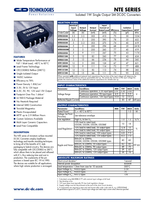
Reflected Ripple Current
TYP 3.30
5 12 30
MAX Units 3.63 5.5 V 13.2
47 mA p-p
OUTPUT CHARACTERISTICS
Parameter
Conditions
Rated Power2
Voltage Set Point Accuracy
元器件交易网
NTE SERIES
Isolated 1W Single Output SM DC-DC Converters
FEATURES s Wide Temperature Performance at
Full 1 Watt Load, –40°C to 85°C s Lead Frame Technology s CECC00802 Reflow (280°C) s Single Isolated Output s 1kVDC Isolation s Efficiency to 78% s Power Density 1.8W/cm3 s 3.3V, 5V & 12V Input s 3.3V, 5V, 9V, 12V and 15V Output s Footprint Over Pins 1.64cm 2 s UL 94V-0 Package Material s No Heatsink Required s Internal SMD Construction s Toroidal Magnetics s Plastic Encapsulated s MTTF up to 2.9 Million Hours s Custom Solutions Available s Multi Layer Ceramic Capacitors s Lead Free Compatible
SES5VT553-5 中文资料
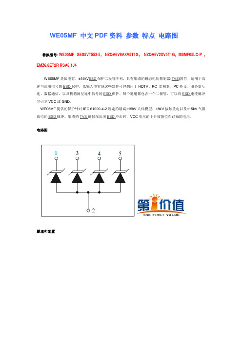
WE05MF 中文PDF资料参数特点电路图
替换型号:WE05MF SES5VT553-5, NZQA6V8AXV5T1G,NZQA6V2XV5T1G,MSMF05LC-P ,EMZ6.8ET2R RSA6.1J4
WE05MF是低电容、±15kV ESD保护二极管阵列,具有集成的瞬态电压抑制器(TVS)箝位,适用于高速与通用信号的ESD保护。
低输入电容使这些器件可理想用于HDTV、PC 监视器、PC外设、服务器互连、数据通信,以及机箱间互连中信号的ESD保护。
每个通道都包含一个二极管,可以将ESD电流脉冲导引到VCC或GND。
WE05MF提供的保护针对IEC 61000-4-2规定的最高±15kV人体模型、±8kV接触放电以及±15kV气隙放电的ESD脉冲。
集成的TVS确保在出现ESD冲击时,VCC电压的上升被箝位在已知的电压。
电路图
原理和配置
电参数
电性能参数
外形图-SOT-553:
尺寸规格
DIM 英寸外型尺寸
Z 0.0708 1.80
G 0.0354 0.90
P 0.0197 TYP 0.50 TYP
X 0.0118 0.3
来源: 第一价值网(IC网络超市)。
华为产品速查手册XXXX版

华为产品速查手册XXXX版全系列产品速查手册华为技术有限公司行业数通产品部2011年6月目录1 NE路由器系列产品11.1 NE 5000E集群路由器11.1.1 NE 5000E集群路由器11.1.2 简介11.1.3 外观11.1.4 关键特性11.1.5 产品规格31.1.6 定购信息41.2 NE 5000E-X16 集群路由器71.2.1 简介71.2.2 外观71.2.3 关键特性71.2.4 产品规格91.2.5 定购信息101.3 NE40E 全业务路由器131.3.1 简介131.3.2 外观131.3.3 关键特性131.3.4 产品规格141.3.5 定购信息161.4 NE20E-X6 高智能业务路由器20 1.4.1 产品概述201.4.2 外观201.4.3 产品特点201.4.4 产品规格231.4.5 定购信息251.5 NE20E/20系列多业务路由器27 1.5.1 产品特点271.5.2 产品规格291.5.3 定购信息302 S系列交换机产品12.1 S9300系列T比特核心路由交换机1 2.1.1 产品特点12.1.2 产品规格42.1.3 配置指南72.1.4 订购信息72.1.5 解决方案应用122.2 S7700系列智能路由交换机 142.2.2 产品规格172.2.3 订购信息202.2.4 解决方案应用232.3 S6700系列万兆交换机242.3.1 产品概述242.3.2 产品特点242.3.3 产品规格282.3.4 组网应用302.3.5 订购信息312.4 S5700系列全千兆企业网交换机32 2.4.1 产品概述322.4.2 产品外观322.4.3 产品特点342.4.4 产品规格372.4.5 组网应用402.4.6 订购信息412.5 S3700系列企业网交换机432.5.1 产品概述432.5.2 产品型号和外观432.5.3 产品特点442.5.4 产品规格482.5.5 组网应用512.5.6 中小型企业网络应用512.5.7 产品选购512.6 S2700系列企业网交换机532.6.1 产品概述532.6.2 产品型号和外观532.6.3 产品特性和优势542.6.5 组网应用582.6.6 订购信息592.7 S1700系列企业网交换机60 2.7.1 产品概述602.7.2 产品型号和外观602.7.3 产品特性和优势602.7.4 产品规格612.7.5 组网应用632.7.6 订购信息633 AR G3产品13.1 AR 3200系列企业路由器1 3.1.1 产品概述13.1.2 关键特性及价值23.1.3 产品规格43.1.4 典型应用53.1.5 选配方式63.2 AR 2200系列企业路由器8 3.2.1 产品概述83.2.2 关键特性及价值93.2.3 产品规格113.2.4 典型应用123.2.5 选配方式143.3 AR 1200系列企业路由器15 3.3.1 产品概述153.3.2 关键特性及价值163.3.3 产品规格183.3.4 典型应用203.3.5 选配方式214 BRAS系列产品14.1 ME60多业务操纵网关1 4.1.1 产品外观24.1.2 关键特性24.1.3 产品规格44.1.4 定购信息65 网管产品15.1 U2000网络治理系统1 5.1.1 产品简介15.1.2 关键特性15.2 华为企业网管eSight 3 5.2.1 产品简介35.2.2 产品特点35.2.3 产品规格55.2.4 产品配置6NE路由器系列产品NE 5000E集群路由器NE 5000E集群路由器简介NE 5000E集群路由器(以下简称NE5000E)是华为公司面向互联网骨干节点、城域网核心节点、数据互联中心节点以及Internet承载节点推出的超级核心路由器产品。
VNH5050A-E;VNH5050ATR-E;中文规格书,Datasheet资料

December 2011Doc ID 16009 Rev 101/33VNH5050A-EAutomotive fully integrated H-bridge motor driverFeatures■Output current: 30A■3V CMOS compatible inputs■Undervoltage and overvoltage shutdown ■Overvoltage clamp ■Thermal shutdown■Cross-conduction protection ■Current and power limitation ■Very low standby power consumption ■PWM operation up to 20 KHz■Protection against loss of ground and loss of V CC■Current sense output proportional to motor current■Output protected against short to ground and short to V CC■Package: ECOP ACK ®DescriptionThe VNH5050A-E is a full bridge motor driver intended for a wide range of automotiveapplications. The device incorporates a dual monolithic high-side driver and two low-side switches. All switches are designed using STMicroelectronics ® well known and proven proprietary VIPower ® M0 technology that allows to efficiently integrate on the same die a true Power MOSFET with an intelligentsignal/protection circuitry. The three dies are assembled in a PowerSSO-36 TP package on electrically isolated lead frames. This package, specifically designed for the harsh automotive environment offers improved thermalperformance thanks to exposed die pads.Moreover, its fully symmetrical mechanical design allows superior manufacturability at board level. The input signals IN A and IN B can directlyinterface to the microcontroller to select the motor direction and the brake condition. The DIAG A /EN A or DIAG B /EN B , when connected to an external pull-up resistor, enables one leg of the bridge. Each DIAG A /EN A provides a digital diagnostic feedback signal as well. The normal operating condition is explained in the truth table. The CS pin allows monitoring the motor current bydelivering a current proportional to its value when CS_DIS pin is driven low or left open. When CS_DIS is driven high, CS pin is in highimpedance condition. The PWM, up to 20KHz, allows to control the speed of the motor in all possible conditions. In all cases, a low level state on the PWM pin turns off both the LS A and LS B switches.Type R DS(on)I out V ccmaxVNH5050A-E50m Ω max (per leg)30A 41VPowerSSO-36 TPTable 1.Device summaryPackageOrder codesTubeTape and reel PowerSSO-36 TP VNH5050A-EVNH5050A TR-EContents VNH5050A-EContents1Block diagram and pin description . . . . . . . . . . . . . . . . . . . . . . . . . . . . . 52Electrical specifications . . . . . . . . . . . . . . . . . . . . . . . . . . . . . . . . . . . . . . 82.1Absolute maximum ratings . . . . . . . . . . . . . . . . . . . . . . . . . . . . . . . . . . . . . 82.2Thermal data . . . . . . . . . . . . . . . . . . . . . . . . . . . . . . . . . . . . . . . . . . . . . . . 92.3Electrical characteristics . . . . . . . . . . . . . . . . . . . . . . . . . . . . . . . . . . . . . . 102.4Waveforms . . . . . . . . . . . . . . . . . . . . . . . . . . . . . . . . . . . . . . . . . . . . . . . . 193Application information . . . . . . . . . . . . . . . . . . . . . . . . . . . . . . . . . . . . . 213.1Reverse battery protection . . . . . . . . . . . . . . . . . . . . . . . . . . . . . . . . . . . . 224Package and PCB thermal data . . . . . . . . . . . . . . . . . . . . . . . . . . . . . . . 244.1PowerSSO-36 thermal data . . . . . . . . . . . . . . . . . . . . . . . . . . . . . . . . . . . 244.1.1Thermal calculation in clockwise and anti-clockwise operation insteady-state mode . . . . . . . . . . . . . . . . . . . . . . . . . . . . . . . . . . . . . . . . . 254.1.2Thermal resistances definition (values according to the PCB heatsinkarea) . . . . . . . . . . . . . . . . . . . . . . . . . . . . . . . . . . . . . . . . . . . . . . . . . . . 254.1.3Thermal calculation in transient mode . . . . . . . . . . . . . . . . . . . . . . . . . . 265Package and packing information . . . . . . . . . . . . . . . . . . . . . . . . . . . . . 295.1ECOPACK® packages . . . . . . . . . . . . . . . . . . . . . . . . . . . . . . . . . . . . . . . 295.2PowerSSO-36 TP package information . . . . . . . . . . . . . . . . . . . . . . . . . . 295.3PowerSSO-36 TP packing information . . . . . . . . . . . . . . . . . . . . . . . . . . . 31 6Revision history . . . . . . . . . . . . . . . . . . . . . . . . . . . . . . . . . . . . . . . . . . . 322/33Doc ID 16009 Rev 10VNH5050A-E List of tables List of tablesTable 1.Device summary. . . . . . . . . . . . . . . . . . . . . . . . . . . . . . . . . . . . . . . . . . . . . . . . . . . . . . . . . . 1 Table 2.Block description. . . . . . . . . . . . . . . . . . . . . . . . . . . . . . . . . . . . . . . . . . . . . . . . . . . . . . . . . . 5 Table 3.Suggested connections for unused and not connected pins . . . . . . . . . . . . . . . . . . . . . . . . 6 Table 4.Pin definitions and functions. . . . . . . . . . . . . . . . . . . . . . . . . . . . . . . . . . . . . . . . . . . . . . . . . 6 Table 5.Pin functions description. . . . . . . . . . . . . . . . . . . . . . . . . . . . . . . . . . . . . . . . . . . . . . . . . . . . 7 Table 6.Absolute maximum ratings. . . . . . . . . . . . . . . . . . . . . . . . . . . . . . . . . . . . . . . . . . . . . . . . . . 8 Table 7.Thermal data. . . . . . . . . . . . . . . . . . . . . . . . . . . . . . . . . . . . . . . . . . . . . . . . . . . . . . . . . . . . . 9 Table 8.Power section. . . . . . . . . . . . . . . . . . . . . . . . . . . . . . . . . . . . . . . . . . . . . . . . . . . . . . . . . . . 10 Table 9.Logic inputs (IN A, IN B, EN A, EN B, PWM, CS_DIS). . . . . . . . . . . . . . . . . . . . . . . . . . . . . . . 11 Table 10.Switching (V CC=13V,R LOAD= 1.5Ω) . . . . . . . . . . . . . . . . . . . . . . . . . . . . . . . . . . . . . . . 11 Table 11.Protections and diagnostics . . . . . . . . . . . . . . . . . . . . . . . . . . . . . . . . . . . . . . . . . . . . . . . . 11 Table 12.Current sense (9 V<V CC<18V). . . . . . . . . . . . . . . . . . . . . . . . . . . . . . . . . . . . . . . . . . . . 12 Table 13.Truth table in normal operating conditions . . . . . . . . . . . . . . . . . . . . . . . . . . . . . . . . . . . . . 17 Table 14.Truth table in fault conditions (detected on OUTA). . . . . . . . . . . . . . . . . . . . . . . . . . . . . . . 17 Table 15.Electrical transient requirements (part 1/3). . . . . . . . . . . . . . . . . . . . . . . . . . . . . . . . . . . . . 18 Table 16.Electrical transient requirements (part 2/3). . . . . . . . . . . . . . . . . . . . . . . . . . . . . . . . . . . . . 18 Table 17.Electrical transient requirements (part 3/3). . . . . . . . . . . . . . . . . . . . . . . . . . . . . . . . . . . . . 18 Table 18.Thermal calculation in clockwise and anti-clockwise operation in steady-state mode . . . . 25 Table 19.Thermal parameters. . . . . . . . . . . . . . . . . . . . . . . . . . . . . . . . . . . . . . . . . . . . . . . . . . . . . . 28 Table 20.PowerSSO-36 TP mechanical data . . . . . . . . . . . . . . . . . . . . . . . . . . . . . . . . . . . . . . . . . . 30 Table 21.Document revision history . . . . . . . . . . . . . . . . . . . . . . . . . . . . . . . . . . . . . . . . . . . . . . . . . 32Doc ID 16009 Rev 103/33List of figures VNH5050A-E List of figuresFigure 1.Block diagram. . . . . . . . . . . . . . . . . . . . . . . . . . . . . . . . . . . . . . . . . . . . . . . . . . . . . . . . . . . . 5 Figure 2.Configuration diagram (top view) . . . . . . . . . . . . . . . . . . . . . . . . . . . . . . . . . . . . . . . . . . . . . 6 Figure 3.Current and voltage conventions . . . . . . . . . . . . . . . . . . . . . . . . . . . . . . . . . . . . . . . . . . . . . 8 Figure 4.Definition of the delay times measurement . . . . . . . . . . . . . . . . . . . . . . . . . . . . . . . . . . . . 14 Figure 5.Definition of the low-side switching times. . . . . . . . . . . . . . . . . . . . . . . . . . . . . . . . . . . . . . 15 Figure 6.Definition of the high-side switching times . . . . . . . . . . . . . . . . . . . . . . . . . . . . . . . . . . . . . 15 Figure 7.Definition of dynamic cross conduction current during a PWM operation. . . . . . . . . . . . . . 16 Figure 8.Definition of delay response time of sense current. . . . . . . . . . . . . . . . . . . . . . . . . . . . . . . 16 Figure 9.Waveforms in full-bridge operation. . . . . . . . . . . . . . . . . . . . . . . . . . . . . . . . . . . . . . . . . . . 19 Figure 10.Waveforms in full-bridge operation (continued) . . . . . . . . . . . . . . . . . . . . . . . . . . . . . . . . . 20 Figure 11.Typical application circuit for DC to 20 kHz PWM operation short circuit protection . . . . . 21 Figure 12.Behavior in fault condition (how a fault can be cleared). . . . . . . . . . . . . . . . . . . . . . . . . . . 22 Figure 13.Half-bridge configuration. . . . . . . . . . . . . . . . . . . . . . . . . . . . . . . . . . . . . . . . . . . . . . . . . . . 23 Figure 14.Multi-motors configuration . . . . . . . . . . . . . . . . . . . . . . . . . . . . . . . . . . . . . . . . . . . . . . . . . 23 Figure 15.PowerSSO-36™ PC board. . . . . . . . . . . . . . . . . . . . . . . . . . . . . . . . . . . . . . . . . . . . . . . . . 24 Figure 16.Chipset configuration . . . . . . . . . . . . . . . . . . . . . . . . . . . . . . . . . . . . . . . . . . . . . . . . . . . . . 25 Figure 17.Auto and mutual R thj-amb vs PCB copper area in open box free air condition . . . . . . . . . . 25 Figure 18.Detailed chipset configuration. . . . . . . . . . . . . . . . . . . . . . . . . . . . . . . . . . . . . . . . . . . . . . . 26 Figure 19.PowerSSO-36 HSD thermal impedance junction ambient single pulse . . . . . . . . . . . . . . . 27 Figure 20.PowerSSO-36 LSD thermal impedance junction ambient single pulse . . . . . . . . . . . . . . . 27 Figure 21.Thermal fitting model of an H-bridge in PowerSSO-36. . . . . . . . . . . . . . . . . . . . . . . . . . . . 28 Figure 22.PowerSSO-36 TP package dimensions. . . . . . . . . . . . . . . . . . . . . . . . . . . . . . . . . . . . . . . 29 Figure 23.PowerSSO-36 TP tube shipment (no suffix). . . . . . . . . . . . . . . . . . . . . . . . . . . . . . . . . . . . 31 Figure 24.PowerSSO-36 TP tape and reel shipment (suffix “TR”) . . . . . . . . . . . . . . . . . . . . . . . . . . . 31 4/33Doc ID 16009 Rev 10VNH5050A-E Block diagram and pin descriptionDoc ID 16009 Rev 105/331 Block diagram and pin descriptionTable 2.Block descriptionNameDescriptionLogic controlAllows the turn-on and the turn-off of the high-side and the low-side switches according to the truth table.Undervoltage/overvoltageShuts down the device for battery voltage outside the range (4,5...24V).High-side and low-side clamp voltage Protect the high-side and the low-side switches from high voltage on the battery line.High-side and low-side driver Drive the gate of the concerned switch to allow a proper R DS(on) for the leg of the bridge.Current limitationLimits the motor current in case of short circuit.High-side and low-side overtemperature protection In case of short-circuit with the increase of the junction temperature, it shuts down the concerned driver to prevent degradation and to protect the die.Low-side overload detectorDetects when low-side current exceeds shutdown current and latches off the concerned low-side.Fault detectionSignalizes an abnormal condition of the switch (output shorted to ground or output shorted to battery) by pulling down the concerned ENx/DIAGx pin.Power limitationLimits the power dissipation of the high-side driver inside safe range in case of short to ground condition.Block diagram and pin descriptionVNH5050A-E6/33Doc ID 16009 Rev 10Table 3.Suggested connections for unused and not connected pinsConnection / pinCurrent sense N.C.SOURCE_HSxDRAIN_LSxINPUTx, PWMDIAGx/ENx CS_DISFloating Not allowed X XX X T o groundThrough 1k Ω resistorXNot allowedXThrough 10k ΩresistorTable 4.Pin definitions and functionsPin N° SymbolFunction13, 24V CC , Heatslug1Drain of high-side switches and power supply voltage.18NC Not connected.15IN A Clockwise input.16EN A /DIAG A Status of high-side and low-side switches A; Open drain output.17IN_PWM PWM input.19CSOutput of current sense.VNH5050A-EBlock diagram and pin descriptionDoc ID 16009 Rev 107/3320CS_DIS Active high CMOS compatible pin to disable current sense pin.21EN B /DIAG BStatus of high-side and low-side switches B; Open drain output.22IN BCounter clockwise input.23, 25, 26, 27, 28, 29, 35OUT B , HeatSlug3Source of high-side switch B / drain of low-side switch B.30, 31, 32, 33, 34,36GND_BSource of low-side switch B.2, 8, 9, 10, 11, 12, 14OUT A, HeatSlug2Source of high-side switch A / drain of low-side switch A.1, 3, 4, 5, 6, 7GND_ASource of low-side switch A.Table 5.Pin functions descriptionName DescriptionV CCBattery connection. GNDPower ground.OUT A OUT B Power connections to the motor.IN A IN B Voltage controlled input pins with hysteresis, CMOS compatible. These two pins control the state of the bridge in normal operation according to the truth table (brake to V CC , Brake to GND, clockwise and counterclockwise).PWMVoltage controlled input pin with hysteresis, CMOS compatible.Gates of low-sideFETS get modulated by the PWM signal during their on phase allowing speed control of the motor.EN A /DIAG A EN B /DIAG BOpen drain bidirectional logic pins.These pins must be connected to an external pull up resistor. When externally pulled low, they disable half-bridge A or B. In case of fault detection (thermal shutdown of a high-side FET or excessive on-state voltage drop across a low-side FET), these pins are pulled low by the device (see truth table in fault condition).CS Analog current sense output. This output delivers a current proportional to the motor current if CS_DIS is low or left open. The information can be read back as an analog voltage across an external resistor.CS_DISActive high CMOS compatible pin to disable the current sense pin.Table 4.Pin definitions and functions (continued)Pin N° Symbol FunctionElectrical specifications VNH5050A-E8/33Doc ID 16009 Rev 102 Electrical specifications2.1 Absolute maximum ratingsTable 6.Absolute maximum ratingsSymbol ParameterValue Unit V CC Supply voltage + 41V I max DC output currentInternally limitedA I R Reverse output current (continuous)(1)1.Based on the internal wires capability.25A I IN Input current (IN A and IN B pins)+/- 10mA I EN Enable input current (DIAG A /EN A and DIAG B /EN B pins)+/- 10mA I pw PWM Input current +/- 10mA I CS_DIS CS_DIS input current+/- 10mA V CS Current sense maximum voltageV CC -41/+V CCV V ESD Electrostatic discharge(Human body model: R =1.5k Ω, C =100pF)2kV T c Junction operating temperature -40 to 150°C T STG Storage temperature-55 to 150 °C I GNDDC reverse ground pin current200mAVNH5050A-E Electrical specificationsDoc ID 16009 Rev 109/332.2 Thermal dataTable 7.Thermal dataSymbol ParameterMax. valueUnit R thj-case Thermal resistance junction-case (per leg)HSD 3.7°C/W LSD3.9°C/W R thj-ambThermal resistance junction-ambientSee Figure 17°C/WElectrical specifications VNH5050A-E10/33Doc ID 16009 Rev 102.3 Electrical characteristicsV CC = 9V up to 18V; -40°C < T j < 150°C, unless otherwise specified.Table 8.Power sectionSymbol ParameterTest conditionsMin.Typ.Max.Unit V CCOperating supply voltage5.518VI SSupply currentOff-state with all fault clearedand ENx =0 (standby) IN A =IN B =PWM =0; T j =25°C; V CC =13V 36µAOff-state with all fault cleared and ENx =0 (standby) V CC =13V;IN A =IN B =PWM =0;T j =-40°C to 150°C10µAOff-state (no standby) IN A =IN B =PWM =0; ENx =5V;T j =-40°C to 150°C 5mAOn-state:IN A or IN B =5V; no PWM 36mAOn-state:IN A or IN B =5V; PWM =20kHz8mA R ONHSStatic high-side resistanceI OUT =8.5A; T j =-40°C17m ΩOUT=8.5A; T j =25°C26m ΩI OUT =8.5A; T j =150°C 52m ΩI OUT =8.5A;T j =- 40°C to 150°C 60m ΩR ONLSStatic low-side resistance I OUT =8.5A; T j =25°C20m ΩIOUT =8.5A;T j =- 40°C to 150°C 40m ΩV fHigh-side free-wheeling diode forward voltageI OUT =-8.5A; T j =150°C0.70.9V I L(off)High-side off-state output current (per channel)T j =25°C; V CC =13V;V OUTX =EN X =0V 03µA T j=125°C; V CC=13V;V OUTX =EN X =0V5µA I RMDynamic cross-conduction currentI OUT =8.5A (see Figure 7)1A分销商库存信息:STMVNH5050A-E VNH5050ATR-E。
N95清晰完整原理图

28 27 29
ACI(1:0) INT_SIM(5:0)
1 0
J2220 J2221 GND GND GND
K4 J4 A6 C6 E7 A5 B6 E6
L2105 240R/100MHz L2106 240R/100MHz
SIM(6:0)
M2100 KHN4NX1RA + C2108 1n0 C2109 1n0 C2110 1n0 GND M -
B2101
4
R2116
via X4401
5 1
LS RFTEMP
GND
GND J2100
C2127 22n 4
C2128 22n
C2126 100n GND
220R/100MHz
1n0
1n0
3.7V
GND
VBAT GND C2228 2/2 1u5 2x1u5
E11 D10 J3 E9 L8 L9 J8 K9
RM-159/RM-245
鼠标移近或点击标注, 即可看到"一品无山"的话
Table of Content
手机设计天下网 到RD3721下载更多资料
Front page AV connector AVilma, Betty Rapido, Memories, GPS Menelaus, microSD OMAP Camera, HWA WLAN, Bluetooth UI, illumination Slide PWB RF part (RM-159) RF part (RM-245) Signal overview Component finder (RM-159) Component finder (RM-245)
service

--------------START_LICENSESERVER LYComputer ANY 27000VENDOR ARCGISFEATURE 3DEngine ARCGIS 10.2 01-jan-0000 2048 AEA2E091990F0E6D001A \vendor_info=TYFJP0FEF40P7PG3T235 ck=242FEATURE Aeronautical ARCGIS 10.2 01-jan-0000 2048 9EB21021133DD2FFD327 \ vendor_info=J3M07HEHGH5NYZCP8086 ck=208FEATURE AGSData ARCGIS 10.2 01-jan-0000 2048 DE22A0F14B97763358A8 \vendor_info=X61NKZH3EJKZ11T04165 ck=28FEATURE AllEurope ARCGIS 10.2 01-jan-0000 2048 AE629041317425F19DCE \vendor_info=TYYRAAH04LXT1FYJX065 ck=22FEATURE ARC/INFO ARCGIS 10.2 01-jan-0000 2048 BE72A0D1C8FA4A4D0DA8 \vendor_info=P12XPAL7JYBSSZ61R019 ck=79FEATURE ArcEditor ARCGIS 10.2 01-jan-0000 2048 DE52A01166A48FBAFC73 \vendor_info=X65XPAJ8484GMBZ7Y018 ck=52FEATURE ArcExpress ARCGIS 10.2 01-jan-0000 2048 DE2280310C465FCF6E9D \vendor_info=X61N53M8NH1E0H5D6049 ck=21FEATURE ArcInfo ARCGIS 10.2 01-jan-0000 2048 DE92B0416DD780188E8B \vendor_info=X6BA9RE2YY0KMEPJL043 ck=254FEATURE ArcMapServer ARCGIS 10.2 01-jan-0000 2048 AEC2D001AFE4A340DA86 \ vendor_info=TY0HZM3L0PYMMR7PN043 ck=23FEATURE ArcPress ARCGIS 10.2 01-jan-0000 2048 9EA200816B9615813F14 \vendor_info=J3LH2PHC711609FFF024 ck=208FEATURE ArcReader ARCGIS 10.2 01-jan-0000 2048 CEA2502143BAFA45FB45 \vendor_info=H3LHA6P80TLRCT8ZZ003 ck=3FEATURE ArcScan ARCGIS 10.2 01-jan-0000 2048 DE82D04178F68B0CA59A \vendor_info=X6A79PH630LLLELZJ222 ck=34FEATURE ArcSdeConnects ARCGIS 10.2 01-jan-0000 2048 8E3290B11B75929C51A9 \ vendor_info=H1HK33ERDXPR0KLM4109 ck=253FEATURE ArcSdeServer ARCGIS 10.2 01-jan-0000 2048 7E02F0510925B615AC36 \ vendor_info=GYL7CZNCHT5FFE67P216 ck=197FEATURE ArcSdl ARCGIS 10.2 01-jan-0000 2048 DE02C0515DA35233DC4A \vendor_info=X6YHHZNC51K2EBYR1143 ck=6FEATURE ArcServer ARCGIS 10.2 01-jan-0000 2048 CE9270210A594A23A67D \vendor_info=H387NL3M37BC561CH246 ck=184FEATURE ArcStorm ARCGIS 10.2 01-jan-0000 2048 8ED20061A45B4D584518 \vendor_info=H1M39HLCS0J2P7XZX033 ck=232FEATURE ArcStormEnable ARCGIS 10.2 01-jan-0000 2048 2EB2D0216F9519381666 \ vendor_info=9K1DF1L6169J6EHHH215 ck=165FEATURE ArcView ARCGIS 10.2 01-jan-0000 2048 CEB2E06163C7D1DF6DAC \vendor_info=H3M04EJELNLCLE2Z3126 ck=125FEATURE ArcView3 ARCGIS 10.2 01-jan-0000 2048 BE320061A45F605A61F5 \vendor_info=P1HKL7ENXBJF7A0JD244 ck=252FEATURE ArcView31 ARCGIS 10.2 01-jan-0000 2048 EEF20081D1BFEF4B2D7A \ vendor_info=Y9Y0PD72LGHM45L73079 ck=61FEATURE ArcView4 ARCGIS 10.2 01-jan-0000 2048 9EF20071B760604F6000 \vendor_info=J3SC06YR98E2P2PPA208 ck=226FEATURE Austria ARCGIS 10.2 01-jan-0000 2048 0EC28001B33C5D422004 \vendor_info=76R6PR7L5HJ8ZK7EB137 ck=250FEATURE AV3D1 ARCGIS 10.2 01-jan-0000 2048 0EC220C1B6316EE1E4CC \vendor_info=76R6F6J0H0C2T064L206 ck=48FEATURE AVArcPress1 ARCGIS 10.2 01-jan-0000 2048 6E82F0D13F061A47CDBA \ vendor_info=FEYPZN3LBEAYKYC76015 ck=6FEATURE Avenue ARCGIS 10.2 01-jan-0000 2048 FEF2C021C7B65236A25E \vendor_info=0K7JRCEH04TJKATN8067 ck=245FEATURE AVIMAGE1 ARCGIS 10.2 01-jan-0000 2048 CE32D051D24804625AEA \vendor_info=H3ZNPAYL92HTJMLPD205 ck=50FEATURE AVIMS1 ARCGIS 10.2 01-jan-0000 2048 3E42D05195B552CEA3D8 \vendor_info=BN078SG55EARS2PEP004 ck=11FEATURE AVIMSGIF ARCGIS 10.2 01-jan-0000 2048 BED2D0E1AF67D6A945CF \vendor_info=P1M35E8E1CSRFM1BB037 ck=30FEATURE AVLAND1 ARCGIS 10.2 01-jan-0000 2048 EE5210F1B13E18BF0072 \vendor_info=Y9807TAEC0JCZKEYM232 ck=222FEATURE AVNetwork1 ARCGIS 10.2 01-jan-0000 2048 8EE270113D6CF3423639 \ vendor_info=H1L6NN5LD53TE6SEZ121 ck=203FEATURE AVNetwork2 ARCGIS 10.2 01-jan-0000 2048 8EF260D13C6BEF433639 \ vendor_info=H1P9PN3LB8AZEDAXT033 ck=5FEATURE AVSpatial1 ARCGIS 10.2 01-jan-0000 2048 FE6250C1F55D5300A160 \ vendor_info=0K0ANEJ5PHYNE0HXP066 ck=172FEATURE AVSpatial2 ARCGIS 10.2 01-jan-0000 2048 BEB280C130985FE9A160 \ vendor_info=P1JHFHPB0PP28TMJJ227 ck=245FEATURE AVSurface1 ARCGIS 10.2 01-jan-0000 2048 AE927001178A47EA5346 \ vendor_info=TY20HES8PD3PXEPY0097 ck=167FEATURE AVSurface2 ARCGIS 10.2 01-jan-0000 2048 6EE2A00152C533F35346 \ vendor_info=FE00XFEE75PHCMHAE116 ck=151FEATURE AVTRACK1 ARCGIS 10.2 01-jan-0000 2048 CED2A0F1CC4AE45963F0 \vendor_info=H3P64M5THAET06NDM070 ck=85FEATURE AVVRP1 ARCGIS 10.2 01-jan-0000 2048 4E02C03194AA50C9AFD9 \vendor_info=CJFMNEEL386BGPSPX066 ck=44FEATURE BaseBISData ARCGIS 10.2 01-jan-0000 2048 4E32D01159CDE893AB96 \ vendor_info=CJK78S8PGEPPSGRP4080 ck=251FEATURE Belgium ARCGIS 10.2 01-jan-0000 2048 EE62B0813CA274165DC5 \vendor_info=Y9A42KEAZS5P0BHLD175 ck=22FEATURE BingMaps ARCGIS 10.2 01-jan-0000 2048 BEB230318C826120583F \vendor_info=P1JH7ZJ5433XP4PDH241 ck=222FEATURE BingMapsEng ARCGIS 10.2 01-jan-0000 2048 1EF210E1C228C71D9BCA \vendor_info=89Y0RHX01YPJEDYBL062 ck=241FEATURE Business ARCGIS 10.2 01-jan-0000 2048 BEB22011A8C468E59F4A \vendor_info=P1JH5HCT704KMBFA8090 ck=19FEATURE BusinessPrem ARCGIS 10.2 01-jan-0000 2048 8E22E041024DB72DEA17 \ vendor_info=H1EHK6SG0JMPM0HK4001 ck=221FEATURE COGO ARCGIS 10.2 01-jan-0000 2048 BE22204135FF4EEEB8B8 \vendor_info=P1EHLBEK1R3PAG13A218 ck=97FEATURE Coverages ARCGIS 10.2 01-jan-0000 2048 CEA240815D9A0B29D728 \vendor_info=H3LH93HRL0KELXC99034 ck=242FEATURE DataReViewer ARCGIS 10.2 01-jan-0000 2048 7E7210A1ED1BC62B9139 \ vendor_info=GYZP0LP5SM5PZPGSH011 ck=15FEATURE DB2 ARCGIS 10.2 01-jan-0000 2048 EEC210D12AD5D7792808 \vendor_info=Y9P9H6L3RGTSCDB2R129 ck=49FEATURE Defense ARCGIS 10.2 01-jan-0000 2048 CE52D0E155AF911351C0 \vendor_info=H32PEHX0BK5PPR2KD030 ck=42FEATURE DefenseINTL ARCGIS 10.2 01-jan-0000 2048 2E7290116BF04BAFB5C8 \vendor_info=9KKEXHBPJ14331A5F024 ck=250FEATURE DefenseINTLEng ARCGIS 10.2 01-jan-0000 2048 6EE2B0113A7BB97A5EB7 \ vendor_info=FE00Z01LB0RLTRPD8010 ck=33FEATURE DefenseUS ARCGIS 10.2 01-jan-0000 2048 CE12B08117776FCFBDE6 \vendor_info=H3HHFHPK520ANTPG1186 ck=67FEATURE DefenseUSEng ARCGIS 10.2 01-jan-0000 2048 FE5260118E9A6839A546 \ vendor_info=0KH7LETD3HF2J3N93125 ck=247FEATURE Denmark ARCGIS 10.2 01-jan-0000 2048 CE12B0F12DBA642A51D8 \vendor_info=H3HHFHE0L0HGEYGJJ225 ck=20FEATURE Designer ARCGIS 10.2 01-jan-0000 2048 AEF20071A990218B76E7 \vendor_info=TYM6CZJKZ0GAPETT8132 ck=240FEATURE DMTIData ARCGIS 10.2 01-jan-0000 2048 9E2200D1AF69406D5408 \vendor_info=J3YKL7L1H63EGTHCZ180 ck=215FEATURE Editor ARCGIS 10.2 01-jan-0000 2048 DEA2A0813EB60E45CE53 \vendor_info=X6L0XFA7XHREBJ8E4031 ck=3FEATURE Foundation ARCGIS 10.2 01-jan-0000 2048 BED2A0B1ED5F74C844A8 \vendor_info=P1M300EBG08ZL49ST179 ck=52FEATURE France ARCGIS 10.2 01-jan-0000 2048 AE52E05160C74933B14C \vendor_info=TYHNRD1RMH4RP0LFJ056 ck=239FEATURE GDBEdit ARCGIS 10.2 01-jan-0000 2048 FE32D0515B8EB6FC599E \vendor_info=0KD02L8HLAG5TB7JN009 ck=42FEATURE GeoStats ARCGIS 10.2 01-jan-0000 2048 7E720061878D424E523B \vendor_info=GYZPY06YRS0AJHPGC250 ck=162FEATURE Germany ARCGIS 10.2 01-jan-0000 2048 1E22A0B1EB9986F25BF6 \vendor_info=894RN3ESF9HSGDZLT058 ck=13FEATURE Grid ARCGIS 10.2 01-jan-0000 2048 BE82409136BD600B77A8 \vendor_info=P140C3XTG5DNBEBB3187 ck=250FEATURE ImageExt ARCGIS 10.2 01-jan-0000 2048 9E8230119D5F7FF03965 \vendor_info=J374D3J1XNYNHSPHF176 ck=10FEATURE Informix ARCGIS 10.2 01-jan-0000 2048 9E82F0D170270DA9091F \vendor_info=J3749YDHPY0C6BTKF059 ck=246FEATURE IntelAgency ARCGIS 10.2 01-jan-0000 2048 1EB2C0C1DD245E55BCB7 \ vendor_info=89S67E5LZCH2MY9T0099 ck=24FEATURE Internal ARCGIS 10.2 01-jan-0000 2048 CE12F04165230D3B1576 \vendor_info=H3HHMAHKFJKSNG1X8066 ck=214FEATURE Interop ARCGIS 10.2 01-jan-0000 2048 1E92E09151F4B2C4B3C6 \vendor_info=89FDH510TS0CEAJ9Z224 ck=233FEATURE InteropEngine ARCGIS 10.2 01-jan-0000 2048 DE2250614D0DB008BC2C \ vendor_info=X61N0TH8ECDPZJP3X023 ck=236FEATURE Italy ARCGIS 10.2 01-jan-0000 2048 6E62F0214C3386CD4C04 \vendor_info=FEENSHZKB3PE062NA046 ck=250FEATURE JTX ARCGIS 10.2 01-jan-0000 2048 EE2210D12AE55D0B4E10 \vendor_info=Y94RX0HC0J5YEFE7S171 ck=190FEATURE Luxembourg ARCGIS 10.2 01-jan-0000 2048 FE92F0C17CE05A97F3A7 \vendor_info=0KNKPDJ7485M0TEDY143 ck=121FEATURE MajorRdEurope ARCGIS 10.2 01-jan-0000 2048 CE8230E1F3B702A65E80 \ vendor_info=H374D3J2RSB8E7L74004 ck=19FEATURE Maplex ARCGIS 10.2 01-jan-0000 2048 BEB2405151CFC6EFB86B \vendor_info=P1JH93JG92TAXNES2208 ck=27FEATURE MaplexEngine ARCGIS 10.2 01-jan-0000 2048 2EE2600145EC2BEDF7DE \ vendor_info=9K5N2ZET07JJF7ELA009 ck=85FEATURE MappingAgency ARCGIS 10.2 01-jan-0000 2048 0EE2F0C1EA1B6DFCDD5B \ vendor_info=76PC0EM6LTJ0JJDBK227 ck=39FEATURE MPSAtlas ARCGIS 10.2 01-jan-0000 2048 AE9240C13C77F5FBB4B2 \vendor_info=TY20C3GELC9CC3HB0005 ck=18FEATURE MrSID ARCGIS 10.2 01-jan-0000 2048 6E62905175160AE92EDD \vendor_info=FEEN77P0C7G4EBERE079 ck=42FEATURE Nautical ARCGIS 10.2 01-jan-0000 2048 BE0260D14EF52BCF0F8D \vendor_info=P1RAL0HC4ZTRGT6MJ033 ck=98FEATURE Netherlands ARCGIS 10.2 01-jan-0000 2048 4E025091587EAA387FDE \ vendor_info=CJFM0YPSMY96KH7LL139 ck=229FEATURE Network ARCGIS 10.2 01-jan-0000 2048 0E92A0F12B66A2EE5BDE \vendor_info=76BA7N6THAAAPAR9L254 ck=88FEATURE NetworkEngine ARCGIS 10.2 01-jan-0000 2048 1E620061ED116824D63A \ vendor_info=89A48TH8SH8FFEJTF168 ck=246FEATURE Plotting ARCGIS 10.2 01-jan-0000 2048 DE824031FC7BF5FA9EA1 \vendor_info=X6A70APF1RJFZTKP7161 ck=41FEATURE Portugal ARCGIS 10.2 01-jan-0000 2048 CE227041FC723D929508 \vendor_info=H3YK0HH5JEF3XT05Y163 ck=235FEATURE Publisher ARCGIS 10.2 01-jan-0000 2048 1E32C05108DC33B28067 \vendor_info=895PPD1RB8ETEEEEL093 ck=36FEATURE Reader ARCGIS 10.2 01-jan-0000 2048 CE92F07146A07FFFBD85 \vendor_info=H387C1PPGMCNF70ML051 ck=53FEATURE ReaderPro ARCGIS 10.2 01-jan-0000 2048 2EA220311F15C20FBCAE \vendor_info=9KZA07JBT9F0GF9M9140 ck=11FEATURE SchematicEngine ARCGIS 10.2 01-jan-0000 2048 DED2C0410F3999D1A7DA \ vendor_info=X6S9AZJB7X20REJ4T191 ck=39FEATURE Schematics ARCGIS 10.2 01-jan-0000 2048 3E22A0F1A95C0F75CDBF \vendor_info=BNF0XASETH2E7RMJE029 ck=61FEATURE SchematicsSDK ARCGIS 10.2 01-jan-0000 2048 9ED26091546DBDC67A00 \ vendor_info=J3P6MKGE7AE2K0FSJ223 ck=251FEATURE SdePersonal ARCGIS 10.2 01-jan-0000 2048 DE521081CF714B1AED89 \vendor_info=X65X3PHBSHNA3X038141 ck=239FEATURE SdeStandard ARCGIS 10.2 01-jan-0000 2048 8E52A0B1A17853952F52 \vendor_info=H1ZRN3ES8HR03MNPA062 ck=180FEATURE SdeWorkGroup ARCGIS 10.2 01-jan-0000 2048 8E7270E138E751690A26 \vendor_info=H12XDAJAZ5966MDM6155 ck=187FEATURE Spain ARCGIS 10.2 01-jan-0000 2048 5E6200518B3E84D34AD7 \vendor_info=DSRKL7TKBY0JAR3A1176 ck=204FEATURE SpatialEngine ARCGIS 10.2 01-jan-0000 2048 7E52D0C1FC887536E51B \ vendor_info=GYHNPAN3SR06RJ2L4181 ck=15FEATURE StandardEngine ARCGIS 10.2 01-jan-0000 2048 DEE260515AE6E921336E \ vendor_info=X6PCSRG6ZS9AZ4HBY137 ck=35FEATURE StreetMap ARCGIS 10.2 01-jan-0000 2048 0E42A0E12518E0A99D7F \vendor_info=764PR6N7EHJGJT4X8064 ck=230FEATURE StreetMapBA ARCGIS 10.2 01-jan-0000 2048 DE628071D29EC3751C23 \vendor_info=X6700081MEJH1LECZ133 ck=214FEATURE Survey ARCGIS 10.2 01-jan-0000 2048 CEE2507152FF80ECCC96 \vendor_info=H3R9NKC6ZXSL0AJ5Y126 ck=254FEATURE SvrAdvanced ARCGIS 10.2 01-jan-0000 2048 8E22606110A6934296ED \vendor_info=H1EHEPD5LXP81N2T5156 ck=202FEATURE SvrEnterprise ARCGIS 10.2 01-jan-0000 2048 2E628081757C8251E783 \ vendor_info=9K0ASPHB40K8P8BRH246 ck=170FEATURE SvrStandard ARCGIS 10.2 01-jan-0000 2048 6E929061CBA341005DD9 \vendor_info=FEZXH07HFXCTLEATB082 ck=205FEATURE Sweden ARCGIS 10.2 01-jan-0000 2048 BEB21061578FBEEABE89 \vendor_info=P1JH4SH826LG4L7DB247 ck=17FEATURE Switzerland ARCGIS 10.2 01-jan-0000 2048 7EF28061AEADAA156752 \vendor_info=GYM6PRHAPG9MKE10N082 ck=47FEATURE Sybase ARCGIS 10.2 01-jan-0000 2048 8E32006174AA80D491A0 \vendor_info=H1HKL7END88CP41GK164 ck=188FEATURE TIFFLZW ARCGIS 10.2 01-jan-0000 2048 DE62A0A1269C591554F6 \vendor_info=X670XDN0LJ1YMMH6E247 ck=0FEATURE TIN ARCGIS 10.2 01-jan-0000 2048 EED23011390255025808 \vendor_info=Y9ECNHYG5AGHLE870145 ck=163FEATURE Tracking ARCGIS 10.2 01-jan-0000 2048 FE1230C143E1EEFB2965 \vendor_info=0KA0PN10AC2R90K2Z202 ck=20FEATURE TrackingEngine ARCGIS 10.2 01-jan-0000 2048 4E6250511C08C01F939D \ vendor_info=CJLHTL8YDPMCESDX4151 ck=234FEATURE UnitedKingdom ARCGIS 10.2 01-jan-0000 2048 8E624001600DD3E067FF \ vendor_info=H11P5HARF0E9GMPZJ070 ck=4FEATURE VBA ARCGIS 10.2 01-jan-0000 2048 EEC290E13407C7F85A10 \vendor_info=Y9P9PYF0JP083JLKT070 ck=13FEATURE Vector ARCGIS 10.2 01-jan-0000 2048 CEF2E051788C7BEDBF67 \vendor_info=H3SCGAEP3C0S3HBS7050 ck=44FEATURE Viewer ARCGIS 10.2 01-jan-0000 2048 EE02106176A77B03C45D \vendor_info=Y91KJBYRHFK4Z818H254 ck=204FEATURE VirtualEarthEng ARCGIS 10.2 01-jan-0000 2048 6E62D0F194C58D675D87 \ vendor_info=FEENPASEFPGCA8HP2223 ck=15END_LICENSE--------------。
DC001NDR5资料

DC001NDR5
Pressure Sensors: Measurement Type: Bidirectional Gage, Differential; Signal Conditioning: Amplified; Pressure Range: ± 1.0 in H2O; Port Style: Barbed
3 of 4
10/31/2005 10:56 AM
Datasheet -- DC001NDR5
元器件交易网
/printfriendly.asp?FAM=pressu...
DC001NDR5
Pressure Sensors: Measurement Type: Bidirectional Gage, Differential; Signal Conditioning: Amplified; Pressure Range: ± 1.0 in H2O; Port Style: Barbed
1 of 4
10/31/2005 10:56 AM
Datasheet -- DC001NDR5
元器件交易网
Compensated Output Calibration Termination Port Style Package Style Typical Sensitivity Full Scale Span Null Offset Offset Position Sensitivity Total Error (% Full Scale) Yes Yes PCB Barbed Honeywell DI-DC 5 V/in H2O ± 2.0 V typ. 3.5 Vdc typ. ± 10 mV
Datasheet -- DC001NDR5
- 1、下载文档前请自行甄别文档内容的完整性,平台不提供额外的编辑、内容补充、找答案等附加服务。
- 2、"仅部分预览"的文档,不可在线预览部分如存在完整性等问题,可反馈申请退款(可完整预览的文档不适用该条件!)。
- 3、如文档侵犯您的权益,请联系客服反馈,我们会尽快为您处理(人工客服工作时间:9:00-18:30)。
H5N5001FMSilicon N Channel MOS FET High Speed Power SwitchingREJ03G1112-0200(Previous: ADE-208-1380)Rev.2.00 Sep 07, 2005Features• Low on-resistance: R DS (on) =1.1 Ω typ.• Low leakage current: I DSS =1 µA max (at V DS = 500 V)• High speed switching: t f = 15ns typ (at V GS = 10 V, V DD = 250 V, I D = 2.5 A) • Low gate charge: Qg = 15nC typ (at V DD = 400 V, V GS = 10 V, I D = 5 A) •Avalanche ratingsOutlineDGSRENESAS Package code: PRSS0003AD-A (Package name: TO-220FM)1. Gate2. Drain3. Source123Absolute Maximum Ratings(Ta = 25°C)Item Symbol Value UnitDrain to source voltage V DSS 500 V Gate to source voltage V GSS ±30 V Drain currentI D 5 A Drain peak currentI D (pulse) Note 120 ABody-drain diode reverse drain current I DR 5 A Body-drain diode reverse drain peak current I DR (pulse) Note 1 20AAvalanche currentI AP Note 3 5AChannel dissipationPch Note 2 30 W Channel to case thermal Impedance θ ch-c 4.17 °C/W Channel temperature Tch 150 °C Storage temperatureTstg–55 to +150°CNotes: 1. PW ≤ 10 µs, duty cycle ≤ 1% 2. Value at Tc = 25°C 3. Tch ≤ 150°CElectrical Characteristics(Ta = 25°C)Item Symbol Min Typ Max Unit Test ConditionsDrain to source breakdown voltage V (BR) DSS 500 — — V I D = 10 mA, V GS = 0 Gate to source leak current I GSS — — ±0.1 µA V GS = ±30 V, V DS = 0 Zero gate voltage drain currentI DSS — — 1 µA V DS = 500 V, V GS = 0 Gate to source cutoff voltageV GS (off) 3.0 — 4.0 V I D = 1 mA, V DS = 10 VStatic drain to source on state resistance R DS (on) — 1.1 1.5 Ω I D = 2.5 A, V GS = 10 V Note 4Forward transfer admittance |y fs | 3.0 4.5 — S I D = 2.5 A, V DS = 10 V Note 4Input capacitance Ciss — 580 — pF Output capacitanceCoss — 70 — pF Reverse transfer capacitance Crss — 13 — pF V DS = 25 V V GS = 0 f = 1 MHz Turn-on delay time t d (on) — 20 — ns Rise timet r — 15 — nsTurn-off delay time t d (off) — 65 — nsFall timet f — 15 — ns I D = 2.5 AV GS = 10 V R L = 100 Ω Rg = 10 Ω Total gate chargeQg— 15 — nC Gate to source chargeQgs—3—nCGate to drain chargeQgd — 8 — nC V DD = 400 V V GS = 10 V I D = 5 ABody-drain diode forward voltage V DF — 0.85 1.3 V I F = 5 A, V GS = 0 Body-drain diode reverse recovery time t rr — 400 — ns Body-drain diode reverse recovery charge Q rr — 1.5 — µC I F = 5 A, V GS = 0 di F /dt = 100 A/µsNote: 4. Pulse testMain Characteristics5010015020013103010010203040501000246824610 VV GS = 4 V4.5 V Tc = 75°C 25°C –25°C6 V5 V8 V5.5 VCase Temperature Tc (°C)Drain to Source Voltage V Gate to Source Voltage V D r a i n C u r r e n t I D (A )Typical Transfer CharacteristicsV DS = 10 V Pulse TestDrain to Source Voltage V DS (V)Typical Output CharacteristicsPulse Test5Drain to Source Saturation Voltage vs.Gate to Source VoltagePulse Tests i s t a n c e (o n ) (Ω)Static Drain to Source on State Resistancevs. Drain Current Pulse TestDrain Current I D (A)Case Temperature Tc (°C)0.3131030100050100150200050001000100200500201610005002050105V f = 1 MHzCissCossCrss I D = 5 AV GSdi / dt = 100 A / µs V GS = 0, Ta = 25°CReverse Drain Current I DR (A)Body-Drain Diode ReverseRecovery TimeTypical Capacitance vs.Drain to Source VoltageC a p a c i t a n c e C (p F )Drain to Source Voltage V (n s )Switching CharacteristicsDynamic Input CharacteristicsV G S (V )V DD = 100 V250 V V GS = 10 V, V DD = 250 V PW = 10 µs, duty ≤ 1 %R G = 10 ΩSource to Drain Voltage V SD (V)Case Temperature Tc (°C)Switching Time Test Circuit Waveform310.30.10.010.030.0010.00310 µ100 µ 1 m 10 m 100 m 1P DMPW TD =PW Tθch – c (t) = γ s (t) • θch – c θch – c = 4.17°C/W, Tc = 25°CTc = 25°CD = 10.50.20.10.050.020.011s h o t pu l se Pulse Width PW (S)N o r m a l i z e d T r a n s i e n t T h e r m a l I m p e d a n c e γ s (t )Normalized Transient Thermal Impedance vs. Pulse WidthPackage Dimensions14.0 ± 1.00.5 ± 0.12.55.0 ±2.0 ± 0.0.7 ± 0.12.54 ± 0.52.54 ± 0.5Ordering InformationPart NameQuantityShipping ContainerH5N5001FM-E 500 pcs Box (Sack)Note: For some grades, production may be terminated. Please contact the Renesas sales office to check the state ofproduction before ordering the product. RENESAS SALES OFFICESRefer to "/en/network" for the latest and detailed information.Renesas Technology America, Inc.450 Holger Way, San Jose, CA 95134-1368, U.S.ATel: <1> (408) 382-7500, Fax: <1> (408) 382-7501Renesas Technology Europe LimitedDukes Meadow, Millboard Road, Bourne End, Buckinghamshire, SL8 5FH, U.K.Tel: <44> (1628) 585-100, Fax: <44> (1628) 585-900Renesas Technology Hong Kong Ltd.7th Floor, North Tower, World Finance Centre, Harbour City, 1 Canton Road, Tsimshatsui, Kowloon, Hong KongTel: <852> 2265-6688, Fax: <852> 2730-6071Renesas Technology Taiwan Co., Ltd.10th Floor, No.99, Fushing North Road, Taipei, TaiwanTel: <886> (2) 2715-2888, Fax: <886> (2) 2713-2999Renesas Technology (Shanghai) Co., Ltd.Unit2607 Ruijing Building, No.205 Maoming Road (S), Shanghai 200020, ChinaTel: <86> (21) 6472-1001, Fax: <86> (21) 6415-2952Renesas Technology Singapore Pte. Ltd.1 Harbour Front Avenue, #06-10, Keppel Bay Tower, Singapore 098632Tel: <65> 6213-0200, Fax: <65> 6278-8001Renesas Technology Korea Co., Ltd.Kukje Center Bldg. 18th Fl., 191, 2-ka, Hangang-ro, Yongsan-ku, Seoul 140-702, KoreaTel: <82> 2-796-3115, Fax: <82> 2-796-2145Renesas Technology Malaysia Sdn. Bhd.Unit 906, Block B, Menara Amcorp, Amcorp Trade Centre, No.18, Jalan Persiaran Barat, 46050 Petaling Jaya, Selangor Darul Ehsan, MalaysiaTel: <603> 7955-9390, Fax: <603> 7955-9510。