RO3073;中文规格书,Datasheet资料
SP300;中文规格书,Datasheet资料

PRODUCT DESCRIPTIONFEATURESTYPICAL APPLICATIONS•Precision Instrumentation Systems •Power Supply Monitoring •Test Boxes•Panel-Mount IndicationORDERING INFORMATIONStock Number Standard MeterSP 300LASCAR ELECTRONICS LTD.MODULE HOUSE WHITEPARISHWILTSHIRE SP52SJ UKTEL:+44(1794)884567FAX:+44(1794)884616E-mail:sales@LASCAR ELECTRONICS INC.PO BOX 50727PALO ALTO CA 94303-0727USATEL:+1(650)8389027FAX:+1(650)8335432E-mail:lascarus@LASCAR ELECTRONICS (HK)LIMITED FLAT C,5/FL.,LUCKY FTY.BLDG.63-65HUNG TO ROAD KWUN TONG KOWLOON HONG KONGTEL:+852********FAX:+852********SP 3003½Digit LED Voltmeter ModuleSAFETYT o comply with the Low V oltage Directive (LVD 93/68/EEC),input voltages to the module’s pins must not exceed 60Vdc.The user must ensure that the incorporation of the panel meter into the user’s equipment conforms to the relevant sections of BS EN 61010(Safety Requirements for Electrical Equipment for Measuring,Control and Laboratory Use).ELECTRICAL SPECIFICATIONS••200mV d.c.Full Scale Reading •50mA @+5V d.c.Power Supply •••Bright Red 9.4mm (0.37")Digit Height Programmable Decimal Points LED Display •Display Blanking Facility •Simplified Connection •Splash ProofAuto-zero and Auto-polarity The SP 300features a 200mV d.c.measurement range with auto-zero and auto-polarity.Decimal points are user selectable.The SP 300features a negative rail generator which enables the meter to measure a signal referenced to its own power supply 0V .The bright red LED display ensures excellent readability under low light conditions.It can be blanked in applications requiring low power operation.The module is easily fitted into the panel,using the fixing clip provided.The module's low cost means it will suit high and low volume applications.The design of the panel meter's housing and seal ensures splash proofing in many applications.SpecificationMin.Typ.Max.UnitAccuracy (overall error)*0.1%(±1count)Linearity ±1count Sample rate2.5samples/secOperating temperature range 050°C Warm-up time10minute Temperature stability 150ppm/°C Supply voltage 4.755 5.25V 50mA Input leakage current (Vin =0V)110pA*To ensure maximum accuracy,re-calibrate periodically.Supply currentPO Box 770, Londonderry, NH 03053 1-800-821-0023PIN FUNCTIONS1.V+Positive power supply to the meter.2.0V 0V power supply connection to the meter. Ground for analogue section of A/D converter.It is actively held at 3.05V (nom)below V+and must not be allowed to sink excessive current (>100A)by,for instance,connecting to a higher voltage.4.IH Positive measuring input.5.IL Negative measuring input.6.DP1Connect to 0V to display DP1(199.9).7.DP2Connect to 0V to display DP2(19.99).8.DP3Connect to 0V to display DP3(1.999).A negative supply is generated internally and mirrors the positive supply.For example:if V+is +5V ,then the internally generated V-is -5V .When measuring with the input referenced to the same supply rail as that of the panel meter,then the limitations on the input range are (V-+1.5V)to (V+-1.5V).LCOM Normally Open.Connects IL to COM.µNote:Solder Links:14532691678分销商库存信息: MARTEL-ELECTRONICS SP300。
SP3072EEN中文资料
DESCRIPTION
The SP3070-3078E differential line transceivers are suitable for bidirectional communication on balanced multipoint bus transmission lines and comply with both RS485 and RS422 EIA Standards. Each device consists of a differential driver and differential receiver. All devices operate from a 3.3V power supply.
VCC 1 R2
8A
R
7B
3
6Z
D
D
4 GND
5Y
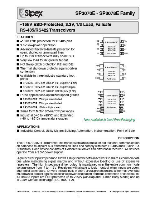
8 Pin Full Duplex: SP3071E, 250kbps slew limited SP3074E, 500kbps slew limited SP3077E, 16Mbps
1 RO RE 2 DE 3
8 VCC R
7B 6A
DI 4
D
open, shorted or terminated lines ■ Up to 256 Transceivers may share Bus ■ Very low load for 8x greater fanout ■ Hot Swap glitch protection RE and DE ■ Thermal shutdown protects against driver
5 GND
8 Pin Half Duplex: SP3072E, 250kbps slew limited SP3075E, 500kbps slew limited SP3078E, 16Mbps
RO2073D中文资料

RF Monolithics, Inc.Phone: (972) 233-2903Fax: (972) 387-8148E-mail: info@ Page 1 of 2RFM Europe Phone: 44 1963 251383Fax: 44 1963 251510 ©1999 by RF Monolithics, Inc. The stylized RFM logo are registered trademarks of RF Monolithics, Inc.RO2073D-040103Electrical CharacteristicsCharacteristicSym Notes Minimum TypicalMaximum Units Frequency (+25 °C)Absolute Frequencyf C 2, 3, 4, 5314.900315.100MHz Tolerance from 315.0MHz∆f C ±100kHz Insertion Loss IL 2, 5, 61.62.5dBQuality Factor Unloaded Q Q U 650050W Loaded Q Q L 1100Temperature StabilityTurnover Temperature T O 6, 7, 8102540°CTurnover Frequencyf O f C Frequency Temperature CoefficientFTC 0.032ppm/°C 2Frequency AgingAbsolute Value during the First Year |f A |1, 610ppm/yr DC Insulation Resistance between Any Two Terminals5 1.0M ΩRF Equivalent RLC ModelMotional Resistance R M 5, 7, 920.6729ΩMotional Inductance L M 67.0µH Motional Capacitance C M 4.00fFShunt Static CapacitanceC O 5, 6, 9 3.5 3.65 4.5pF Test Fixture Shunt Inductance L TEST2, 764.6nHLid Symbolization442 // YWWSStandard Reel Quantity Reel Size 7 Inch 500 Pieces / Reel Reel Size 13 Inch 3000 Pieces / Reel•Ideal for 315MHz Automotive-Keyless-Entry Transmitters •Very Low Series Resistance•Quartz Stability•Complies with Directive 2002/95/EC (RoHS)The RO2073D is a true one-port, surface-acoustic-wave (SAW) resonator in a surface-mount, ceramic case.It provides reliable, fundamental-mode, quartz frequency stabilization of local oscillators operating at approx-imately 315MHz. This SAW was designed for AM transmitters in automotive-keyless-entry applications operating in the USA under FCC Part 15, in Canada under DoC RSS-210, and in Italy.Absolute Maximum RatingsRatingValue Units Input Power Level 0dBm DC Voltage12VDC Storage Temperature-40 to +85°C Soldering Temperature (10 seconds / 5 cycles max.)260°C315.0 MHz SAW ResonatorRO2073D CAUTION: Electrostatic Sensitive Device. Observe precautions for handling.Notes:1.Frequency aging is the change in f C with time and is specified at +65°C or less. Aging may exceed the specification for prolonged temperatures above +65°C. Typically, aging is greatest the first year after manufacture, decreasing in subse-quent years.2.The center frequency, f C , is measured at the minimum insertion loss point, IL MIN , with the resonator in the 50Ω test system (VSWR ≤ 1.2:1). The shunt inductance, L TEST , is tuned for parallel resonance with C O at f C . Typically, f OS-CILLATOR or f TRANSMITTER is approximately equal to the resonator f C .3.One or more of the following United States patents apply: 4,454,488 and 4,616,197.4.Typically, equipment utilizing this device requires emissions testing and govern-ment approval, which is the responsibility of the equipment manufacturer.5.Unless noted otherwise, case temperature T C =+25°C±2°C.6.The design, manufacturing process, and specifications of this device are subject to change without notice.7.Derived mathematically from one or more of the following directly measured parameters: f C , IL, 3dB bandwidth, f C versus T C , and C O .8.Turnover temperature, T O , is the temperature of maximum (or turnover) fre-quency, f O . The nominal frequency at any case temperature, T C , may be calcu-lated from: f =f O [1-FTC (T O -T C )2]. Typically oscillator T O is approximately equal to the specified resonator T O .9.This equivalent RLC model approximates resonator performance near the reso-nant frequency and is provided for reference only. The capacitance C O is the static (nonmotional) capacitance between the two terminals measured at low frequency (10MHz) with a capacitance meter. The measurement includes para-sitic capacitance with "NC” pads unconnected. Case parasitic capacitance is approximately 0.05pF. Transducer parallel capacitance can by calculated as: C P ≈C O -0.05pF.Pb315.0 MHz SAW ResonatorRF Monolithics, Inc.Phone: (972) 233-2903Fax: (972) 387-8148E-mail: info@ Page 2 of 2RFM Europe Phone: 44 1963 251383Fax: 44 1963 251510 ©1999 by RF Monolithics, Inc. The stylized RFM logo are registered trademarks of RF Monolithics, Inc.RO2073D-040103Case DimensionsEquivalent LC Mode lTemperature CharacteristicsThe curve shown on the right accounts for resonator contribution only and does not include LC component temperature contributions .Pin Connection1NC 2Terminal 3NC 4NC 5Terminal 6NCPower TestElectrical ConnectionsThe SAW resonator is bidirectional and may be installed with either orientation.The two terminals are interchangeable and unnumbered. The callout NC indi-cates no internal connection. The NC pads assist with mechanical positioning and stability. External grounding of the NC pads is recommended to help reduce parasitic capacitance in the circuit.Typical Test CircuitThe test circuit inductor, L TEST , is tuned to resonate with the static capacitance, C O , at F C .Electrical TestTypical Application CircuitsDimensionmm Inches Min Nom Max Min Nom Max A 3.60 3.80 4.00.140.150.16B 3.60 3.80 4.00.140.150.16C 1.00 1.20 1.400.040.050.055D 0.95 1.10 1.250.0370.0430.05E 2.39 2.54 2.690.0900.100.110G 0.90 1.0 1.100.0350.040.043H 1.90 2.0 2.100.750.080.83I 0.500.60.700.0200.0240.028J1.701.81.900.0670.070.075。
SP3077EMN中文资料

VCC 1 R2
8A
R
7B
3
6Z
D
D
4 GND
5Y
8 Pin Full Duplex: SP3071E, 250kbps slew limited SP3074E, 500kbps slew limited SP3077E, 16Mbps
1 RO RE 2 DE 3
8 VCC R
7B 6A
DI 4
D
ELECTRICAL CHARACTERISTICS
Unless otherwise noted VCC = +3.3 ±0.3V, ambient temperature TMIN < TA < TMAX. Typical values are at VCC = 3.3, ambient temperature TA = +25ºC. The ♦ denotes the specifications which apply over the full operating range unless otherwise noted.
2
SP3074EEN资料

DESCRIPTIONAPPLICATIONS■Industrial Control, Utility Meters Building Automation, Instrumentation, Point of Sale The SP3070-3078E differential line transceivers are suitable for bidirectional communication on balanced multipoint bus transmission lines and comply with both RS485 and RS422 EIA Standards. Each device consists of a differential driver and differential receiver. All devices operate from a 3.3V power supply.High receiver input impedance allows a large number of transceivers to share a common data bus while maintaining signal margin and without excessive loading or use of expensive repeaters. The high impedance driver output is maintained over the entire common-mode voltage range from -7 to +12V. Receivers will failsafe to logic 1 output when inputs are open,shorted or terminated. Drivers include built-in short-circuit protection and a thermal-overload shutdown to protect against excessive power dissipation from bus contention or cable faults.All RS485 inputs are ESD protected up to ±15kV (Air-Gap and Human Body Model) and up to ±8kV Contact discharge (IEC 1000-4-2).DEVICE ARCHITECTURE AND BLOCK DIAGRAMSCCZZCC 14 Pin Full Duplex:SP3070E, 250kbps slew limited SP3073E, 500kbps slew limited SP3076E, 16Mbps8 Pin Full Duplex:SP3071E, 250kbps slew limited SP3074E, 500kbps slew limited SP3077E, 16Mbps8 Pin Half Duplex:SP3072E, 250kbps slew limited SP3075E, 500kbps slew limited SP3078E, 16MbpsDevices are available in three industry standard architectures and footprints. In each footprint there are three speed grades available.These are stress ratings only and functional operation of the device at these ratings or any other above those indicated in the operation sections of the specifications below is not implied. Exposure to absolute maximum rating conditions for extended periods of time may affect reliability.V CC .....................................................................................................+6.0V Input Voltage at control input pins (RE, DE).........................-0.3V to 6V Driver Input Voltage (RE, DE)...............................................-0.3V to 6V Driver Output Voltage (A, B, Y, & Z)....................................-8V to +13V Receiver Input Voltage (A, B)..............................................-8V to +13VELECTRICAL CHARACTERISTICSABSOLUTE MAXIMUM RATINGSUnless otherwise noted V CC = +3.3 ±0.3V, ambient temperature T MIN < T A < T MAX . Typical values are at V CC = 3.3,ambient temperature T A = +25ºC. The ♦ denotes the specifications which apply over the full operating range unless otherwise noted.Continuous Power Dissipation at Ta = 70o C8-pin SO (derate 5.88mW/o C above +70o C)................................471mW 8-pin PDIP (derate 9.29mW/o C above +70o C)............................727mW 14-pin SO (derate 8.33mW/o C above +70o C).............. .............667mW 14-pin PDIP (derate 10mW/o C above +70o C).................. ..........800mW Operating Temperature RangesSP307_EMN.................................................................-40ºC to +125ºC SP307_EEN ...............................................................-40ºC to +85ºC Junction Temperature............................................................. ..+150ºC Storage Temperature Range..........................................-65ºC to +150º C Lead Temperature (soldering, 10s) ........................................... +300º CRE T E M A R A P .M Y S .N I M .P Y T .X A M ST I N U ♦SN O I T I D N O C tu p t u O r e v i r D l a i t n e r e f f i D V DO 2V C C V1e r u g i F ,)224-S R (Ω001=L R 5.1V C C 1e r u g i F ,)584-S R (Ω45=L R V CC ♦da o L o N f o e d u t i n g a M n i e g n a h C e g a t l o V t u p t u O l a i t n e r e f f i D V ∆D O 2.0V ♦1e r u g i F ,Ω001r o 45=L R t u p t u O e d o M n o m m o C r e v i r D eg a t l o V V CO V C C 2/3V ♦1e r u g i F ,Ω001r o 45=L Rf o e d u t i ng a M n i e g n ah C t u p t u O e d o M n o m m o C eg a t l o V V ∆C O 2.0±V 1e r u g i F ,Ω001r o 45=L R e g a t l o V h g i H t u p n I V H I 2V♦E R ,I D ,E D e g a t l o V w o L t u p n I V L I 8.0V E R ,I D ,E D s i s e r e t s y H t u p n I V S Y H 001Vm ♦E R ,I D ,E D t n e r r u C t u p n I I NI 1-1A µ♦ER ,I D ,E D t s r i F e c n a d e p m I t u p n I )p a w s t o H (n o i t i s n a r T 101Ωk ♦ER ,E D e r o m w a r d l l i w n o i t i s n a r t t s r i F )p a w s t o H (t n e r r u c )Z d n a Y (e g a k a e L t u p t u O )B d n a A (x e l p u D l l u F I O521+Aµ♦DN G =E D V C C V6.3r o D N G =V N I V 21+=001-♦V N I V7-=tn e r r u C t i u c r i C -t r o h S r e v i r D I DS O 0052±Am V ≤V 7-T U O )A 4e r u g i F (,V 21≤052-0ELECTRICAL CHARACTERISTICSUnless otherwise noted V CC = +3.3 ±0.3V, ambient temperature T MIN < T A < T MAX . Typical values are at V CC = 3.3,ambient temperature T A = +25ºC. The ♦ denotes the specifications which apply over the full operating range unless otherwise noted.SR E T E M A R A P M Y S N I M P Y T X A M S T I N U ♦SN O I T I D N O C )B d n a A (t n e r r u C t u p n I xe l p u Df l a H I B,A 521Aµ♦DN G =E D V C C 6.3r o D N G =V N I V 21+=001-V N I V7-=d l o h s e r h T n w o d t u h S -l a m r e h T T S T 561C º♦s i s e r e t s y H n w o d t u h S l a m r e h T T HS T 51Cº♦RE V I E C E R d l o h s e r h T l a i t n e r e f f i D r e v i e c e R )y t i v i t i s n e S (V H T 002-521-05-V m ≤V 7-V M C V 21≤s i s e r e t s y H t u p n I r e v i e c e R V ∆H T 51V m ♦V 0=b V +a V e g a t l o V h g i H t u p t u O O R V H O -c c V 6.0V♦I O A m 1-=e g a t l o V w o L t u p t u O O R V L O 4.0V ♦I O A m 1=t a t n e r r u C t u p t u O e t a t S -i r T re v i e c e R I R Z O 1-/+A µ♦V ≤0O V ≤C C e c n a t s i s e R t u p n I r e v i e c e R R N I 69Ωk ♦V ≤V 7-M C V 21≤t i u c r i C -t r o h S t u p t u O r e v i e c e R tn e r r u C I RZ O 06±Am V ≤V 0O R V ≤CC TN E R R U C Y L P P U S tn e r r u C y l p p u S I CC 8.05.1Am ♦V =E D ,0=E R ,d a o L o N C C 8.05.1V =E R ,d a o L o N C C V =E D ,C C 8.05.10=E D ,0=E R ,d a o L o N n w o d t u h S n i t n e r r u C y l p p u S ed o m I ND H S 50.03A µV =E R C C DN G =E D ,NO I T C E T O R P D S E Bd n a ,A ,Z ,Y r o f n o i t ce t o r P D S E 51±Vk ♦le d o M y d o B n a m u H 51±)2-4-0001C E I (p a G r i A 8±)2-4-0001C E I (t c a t n o CRECEIVER SWITCHING CHARACTERISTICSDRIVER SWITCHING CHARACTERISTICSS C I T S I R E T C A R A H C G N I H C T I W S R E V I R D E 2703P S &E 1703P S ,E 0703P S RE T E M A R A P L O B M Y S .N I M .P Y T .X A M S T I N U S N O I T I D N O C y a l e D n o i t a g a p o r P r e v i r D t H L P D 052-0051s n C L R ,F p 05=L ,Ω45=3&2e r u g i F t L H P D 052-0051s n r o e s i R t u p t u O l a i t n e r e f f i D r e v i r D em i T l l a F t ,R D t F D 053-0061s n C L R ,F p 05=L ,Ω45=3&2e r u g i F w e k S t u p t u O l a i t n e r e f f i D r e v i r D t (H L P D t -L H P D )t WE K S D --002s n C L R ,F p 05=L ,Ω45=3&2e r u g i F e t a R a t a D m u m i x a M 052--s p b k h g i H t u p t u O o t e l b a n E r e v i r D t H Z D --0052s n 4e r u g i F w o L t u p t u O o t e l b a n E r e v i r D t L Z D --0052s n 5e r u g i F w o L m o r f e m i T e l b a s i D r e v i r D t Z L D --001s n 5e r u g i F h g i H m o r f e m i T e l b a s i D r e v i r D t Z H D --001s n 4e r u g i F o t n w o d t u h S m o r f e l b a n E r e v i r D hg i H t u p t u O t )N D H S (H Z D --0055s n 4e r u g i F o t n w o d t u h S m o r f e l b a n E r e v i r D w o L t u p t u O t )N D H S (L Z D --0055s n 5e r u g i F nw o d t u h S o t e m i T t N D H S 05002006sn Unless otherwise noted V CC = +3.3 ±0.3V, ambient temperature T MIN < T A < T MAX . Typical values are at V CC = 3.3,ambient temperature T A = +25ºC.Unless otherwise noted V CC = +3.3 ±0.3V, ambient temperature T MIN < T A < T MAX . Typical values are at V CC = 3.3,ambient temperature T A = +25ºC.2703P S &1703P S ,0703P S s c i t s i r e t c a r a h C g n i h c t i w S r e v i e c e R RE T E M A R A P L O B M Y S .N I M .P Y T .X A M S T I N U S N O I T I D N O C y a l e D n o i t a g a p o r P r e v i e c e R t H L P R --002s n C L 7&6e r u g iF ,F p 51=t L H P R --002s n t (w e k S t u p t u O r e v i e c e R H L P D t -L H P D )t WE K S R --03s n C L 7&6e r u g i F ,F p 51=et a R a t a D 052--s p b k h g i H t u p t u O o t e l b a n E r e v i e c e R t H Z R --05s n 8e r u g i F w o L t u p t u O o t e l b a n E r e v i e c e R t L Z R --05s n 8e r u g i F w o L m o r f e m i T e l b a s i D r e v i e c e R t Z L R --002s n 8e r u g i F h g i H m o r f e m i T e l b a s i D r e v i e c e R t Z H R --001s n 8e r u g i F o t n w o d t u h S m o r f e l b a n E r e v i e c e R hg i H t u p t u O t )N D H S (H Z R --0004s n 8e r u g i F o t n w o d t u h S m o r f e l b a n E r e v i e c e R wo L t u p t t u O t )N D H S (L Z R --0004sn 8e r u g i FRECEIVER SWITCHING CHARACTERISTICSDRIVER SWITCHING CHARACTERISTICSUnless otherwise noted V CC = +3.3 ±0.3V, ambient temperature T MIN < T A < T MAX . Typical values are at V CC = 3.3,ambient temperature T A = +25ºC.Unless otherwise noted V CC = +3.3 ±0.3V, ambient temperature T MIN < T A < T MAX . Typical values are at V CC = 3.3,ambient temperature T A = +25ºC.5703P S &4703P S ,3703P S s c i t s i r e t c a r a h C g n i h c t i w S r e v i e c e R RE T E M A R A P L O B M Y S .N I M .P Y T .X A M S T I N U S N O I T I D N O C y a l e D n o i t a g a p o r P r e v i e c e R t H L P R --002s n C L 7&6e r u g iF ,F p 51=t L H P R --002s n t (w e k S t u p t u O r e v i e c e R H L P D t -L H P D )t WE K S R --03s n C L 7&6e r u g i F ,F p 51=et a R a t a D m u m i x a M 005--s p b k h g i H t u p t u O o t e l b a n E r e v i e c e R t H Z R --05s n 8e r u g i F w o L t u p t u O o t e l b a n E r e v i e c e R t L Z R --05s n 8e r u g i F w o L m o r f e m i T e l b a s i D r e v i e c e R t Z L R --05s n 8e r u g i F h g i H m o r f e m i T e l b a s i D r e v i e c e R t Z H R --05s n 8e r u g i F o t n w o d t u h S m o r f e l b a n E r e v i e c e R hg i H t u p t u O t )N D H S (H Z R --0004s n 8e r u g i F o t n w o d t u h S m o r f e l b a n E r e v i e c e R w o L t u p t t u O t )N D H S (L Z R --0004s n 8e r u g i F S C I T S I R E T C A R A H C G N I H C T I W S R E V I R D E 5703P S &E 4703P S ,E 3703P S RE T E M A R A P L O B M Y S .N I M .P Y T .X A M S T I N U S N O I T I D N O C y a l e D n o i t a g a p o r P r e v i r D t H L P D 081-008s n C L R ,F p 05=L ,Ω45=3&2e r u g i F t L H P D 081-008s n r o e s i R t u p t u O l a i t n e r e f f i D r e v i r D em i T l l a F t ,R D t F D 002-008s n C L R ,F p 05=L ,Ω45=3&2e r u g i F w e k S t u p t u O l a i t n e r e f f i D r e v i r D t (H L P D t -L H P D )t WE K S D --001s n C L R ,F p 05=L ,Ω45=3&2e r u g i F et a R a t a D 005--s p b k h g i H t u p t u O o t e l b a n E r e v i r D t H Z D --0052s n 4e r u g i F w o L t u p t u O o t e l b a n E r e v i r D t L Z D --0052s n 5e r u g i F w o L m o r f e m i T e l b a s i D r e v i r D t Z L D --001s n 5e r u g i F h g i H m o r f e m i T e l b a s i D r e v i r D t Z H D --001s n 4e r u g i F o t n w o d t u h S m o r f e l b a n E r e v i r D hg i H t u p t u O t )N D H S (H Z D --0054s n 4e r u g i F o t n w o d t u h S m o r f e l b a n E r e v i r D w o L t u p t u O t )N D H S (L Z D --0054s n 5e r u g i F nw o d t u h S o t e m i T t N D H S 05002006snDRIVER SWITCHING CHARACTERISTICSUnless otherwise noted Vcc=+3.3±0.3V, ambient temperature Tmin < Ta < Tmax. Typical values are at Vcc = 3.3,ambient temperature Ta = +25ºCRECEIVER SWITCHING CHARACTERISTICSUnless otherwise noted Vcc=+3.3±0.3V, ambient temperature Tmin < Ta < Tmax. Typical values are at Vcc = 3.3,ambient temperature Ta = +25ºCS C I T S I R E T C A R A H C G N I H C T I W S R E V I R D E 8703P S &E 7703P S ,E 6703P S RE T E M A R A P L O B M Y S .N I M .P Y T .X A M S T I N U SN O I T I D N O C y a l e D n o i t a g a p o r P r e v i r D t H L P D --05s n C L R ,F p 05=L ,Ω45=3&2e r u g i F t L H P D --05s n r o e s i R t u p t u O l a i t n e r e f f i D r e v i r D em i T l l a F t ,R D t F D --51s n C L R ,F p 05=L ,Ω45=3&2e r u g i F w e k S t u p t u O l a i t n e r e f f i D r e v i r D t (H L P D t -L H P D )t WE K S D --8s n C L R ,F p 05=L ,Ω45=3&2e r u g i F et a R a t a D 61--s p b M h g i H t u p t u O o t e l b a n E r e v i r D t H Z D --051s n 4e r u g i F w o L t u p t u O o t e l b a n E r e v i r D t L Z D --051s n 5e r u g i F w o L m o r f e m i T e l b a s i D r e v i r D t Z L D --001s n 5e r u g i F h g i H m o r f e m i T e l b a s i D r e v i r D t Z H D --001s n 4e r u g i F o t n w o d t u h S m o r f e l b a n E r e v i r D hg i H t u p t u O t )N D H S (H Z D --0081s n 4e r u g i F o t n w o d t u h S m o r f e l b a n E r e v i r D w o L t u p t u O t )N D H S (L Z D --0081s n 5e r u g i F nw o d t u h S o t e m i T t N D H S 05002006sn 8703P S &7703P S ,6703P S s c i t s i r e t c a r a h C g n i h c t i w S r e v i e c e R RE T E M A R A P L O B M Y S .N I M .P Y T .X A M S T I N U S N O I T I D N O C y a l e D n o i t a g a p o r P r e v i e c e R t H L P R -0457s n C L ,7&6e r u g iF ,F p 51=Cº58+o t 04-t L H P R -0457s n t (w e k S t u p t u O r e v i e c e R H L P D t -L H P D )t WE K S R --8s n C L ,7&6e r u g i F ,F p 51=et a R a t a D 61--s p b M h g i H t u p t u O o t e l b a n E r e v i e c e R t H Z R --06s n C º58+o t 04-,8e r u g i F w o L t u p t u O o t e l b a n E r e v i e c e R t L Z R --06s n C º58+o t 04-,8e r u g i F w o L m o r f e m i T e l b a s i D r e v i e c e R t Z L R --05s n 8e r u g i F h g i H m o r f e m i T e l b a s i D r e v i e c e R t Z H R --05s n 8e r u g i F o t n w o d t u h S m o r f e l b a n E r e v i e c e R hg i H t u p t u O t )N D H S (H Z R --0081s n 8e r u g i F o t n w o d t u h S m o r f e l b a n E r e v i e c e R w o L t u p t u O t )N D H S (L Z R --0081s n 8e r u g i F 元器件交易网FIGURE 3. DRIVER PROPAGATION DELAY TIME TEST CIRCUIT AND TIMING DIAGRAMFIGURE 1. DRIVER DC TEST CIRCUITFIGURE 2. RECEIVER DC TEST CIRCUITDI V DIFFV V D I0 or 3VΩOUTDEDI = 0 or 3VDE = 0 or 3V FIGURE 4A. DRIVER CONTENTION TESTFIGURE 6. RECEIVER PROPAGATION DELAY TEST CIRCUIT & TIMING DIAGRAMV CCVL V OLOH A BΩOUTFIGURE 8. RECEIVER ENABLE & DISABLE TIMING DIAGRAMFIGURE 7. RECEIVER ENABLE & DISABLE TIMES TEST CIRCUIT1.5V -1.5VCCCCS1 is closed, S2 is open, S3 = -1.5VOLCCS1 is closed, S2 is open, S3 = -1.5VOLS1 is open S2 is closed S3 = 1.5VOHS1 is open S2 is closed S3 = 1.5VFUNCTION TABLES)xe l puDl l uF(E673PS,E373PS,E73PSGN I TT IMSNARTs t upn I s t up t uOER ED I D Z Y X1101 X1010 00X Z-hg i H10X nwod t uhS)xe l puDl l uF(E673PS,E373PS,E73PSGN I V I ECERs t upn I t up t uOER ED B,A OR0X Vm5-≥10X Vm2-≤0X X,nepOde t r ohS111X Z-hg i H10X nwod t uhS)xe l puDf l aH(E873PS,E573PS,E273PSGN I TT IMSNARTs t upn I s t up t uOER ED I D Z/B Y/A X1101 X1010 00X Z-hg i H10X nwod t uhS)xe l puDf l aH(E873PS,E573PS,E273PSGN I V I ECERs t upn I t up t uOER ED B,A OR0X Vm5-≥10X Vm2-≤0X X de t r oh s/nepO111X Z-hg i H10X nwod t uhS)xe l puDl l uF(E773PS,E473PS,E173PSGN I TT IMSNARTs t upn I s t up t uOI D Z Y101010)xe l puDl l uF(E773PS,E473PS,E173PSGN I V I ECERs t upn I t up t uOB,A ORVm5-≥1Vm2-≤0de t r oh s/nepO1PIN DESCRIPTIONXELPUDLLUFSEC I VEDFLAHXELPUDSEC I VEDN I PEMANNO I TCNUFN I PE73PS E173PS E273PSE373PS E473PS E573PSE673PS E773PS E873PSREBMUNN I P221OR≥)B–A(f i dnawo l s iERnehW.t up t uOr e v i e c eR.wo l s iOR,Vm2-≤)B–A(f I.hg i Hs iOR,Vm5-3-2ER.de l banes iOR,wo l s iERnehW.e l banEt up t uOr e v i e c eRebd l uoh sER.e c nadepm i hg i hs iOR,hg i hs iERnehW-t ohas iER.edomnwod t uh sr e t neo two lEDdnahg i h.t upn i paws4-3EDe r as t up t uo,hg i hs iEDnehW.e l banEt up t uOr e v i r DED.e c nadepm i hg i he r as t up t uo,wo l s iEDnehW.de l banes iED.edomnwod t uh sr e t neo thg i hERdnawo l ebd l uoh s.t upn i paws-t oha534I Ds e c r o f I Dno l e v e lwo l a,hg i hEDh t iW.t upn I r e v i r D,y l r a l i m i S.hg i ht up t uogn i t r e v n i dnawo l t up t uogn i t r e v n i nondnahg i ht up t uogn i t r e v n i nons e c r o f I Dno l e v e l hg i ha.wo l t up t uogn i t r e v n i7,645DNG dnuo rG95-Y t up t uOr e v i r Dgn i t r e v n i noN16-Z t up t uOr e v i r Dgn i t r e v n I117-B t upn I r e v i e c eRgn i t r e v n I--7B t up t uOr e v i r Dgn i t r e v n Idnat upn I r e v i e c eRgn i t r e v n I218-A t upn I r e v i e c eRgn i t r e v n i noN--6Ar e v i r Dgn i t r e v n i noNdnat upn I r e v i e c eRgn i t r e v n i noNt up t uO4118VCCy l ppuSe v i t i s oP VCCs s ap yB.VCCFu1.0ah t i wDNGo t.r o t i c apa c31,8,1--CN t c ennoCoNDETAILED DESCRIPTIONThe SP307XE family of high speed transceiv-ers for RS-485/RS-422 communication con-tain one driver and one receiver. These devices feature fail-safe circuitry, which guar-antees a logic-high receiver output when the receiver inputs are open or shorted, or when they are connected to a terminated transmis-sion line with all drivers disabled. The SP3070E, SP3072E, SP3073E, SP3075E, SP3076E and SP3078E also feature a hotswap capability allowing live insertion with-out error data transfer. The SP3070E, SP3071E and SP3072E feature reduced slew-rate drivers that minimize EMI and reduce reflections caused by improperly terminated cables, allowing error-free data transmission up to 250kbps. The SP3073E, SP3074E and SP3075E also offer slew -rate limits allowing transmit speeds up to 500kbps. The SP3076E, SP3077E, SP3078E driver slew rates are not limited, making transmit speeds up to 16Mbps possible.The SP3072E, SP3075E and SP3078E are half-duplex transceivers, while the SP3070E, SP3071E, SP3073E, SP3074E, SP3076E, and SP3077E are full duplex transceivers. All devices operate from a single 3.3V supply. Drivers are output short-circuit current limited. Thermal-shutdown circuitry protects drivers against excessive power dissipation. When activated, the thermal-shutdown circuitry places the driver outputs into a high-imped-ance state.RECEIVER INPUT FILTERINGSP3070-SP3075 receivers incorporate input filtering in addition to input hysteresis. This filtering enhances noise immunity with differ-ential signals that have very slow rise and fall times. Receiver propagation delay increases by 25% due to this filtering.FAIL SAFEThe SP3070 family guarantees a logic-high receiver output when the receiver inputs are shorted, open, or when they are connected to a terminated transmission line with all drivers disabled. If A - B is less than or equal to -200mV, RO is logic low. In the case of a terminated bus with all transmitters disabled the receiver's differential input voltage is pulled to 0V by the termination. With the receiver thresholds of the SP3070E family, this results in a logic high with a 50mV minimum noise margin. In compliance with the EIA/TIA-485 standard, the SP3070E family has a 50mV -200mV threshold.HOT-SWAP CAPABILITYWhen circuit boards are inserted into a hot backplane, differential disturbances to the data bus can lead to data errors. Upon initial circuit board insertion, the data communica-tion processor undergoes its own power-up sequence. During this period, the processor's logic-output drivers are high impedance and are unable to drive the DE and RE inputs of these devices to a defined logic level. Leak-age currents up to 10µA from the high-imped-ance state of the processor's logic drivers could cause standard CMOS enable inputs of a transceiver to drift to an incorrect logic level. Additionally, parasitic circuit board capaci-tance could cause coupling of VCC or GND to the enable inputs. Without the hot-swap capa-bility, these factors could improperly enable the transceiver's driver or receiver.When VCC rises, an internal pulldown circuit holds DE low and RE high for approximately 10 microseconds. After the initial power-up sequence, the pulldown circuit becomes trans-parent, resetting the hot-swap tolerable input. 15KV ESD PROTECTIONAs with all Sipex devices, ESD-protection structures are incorporated on all pins to protect against electrostatic discharges en-countered during handling and assembly. The driver output and receiver inputs of the SP3070E family of devices have extra protec-tion against static electricity. Sipex's engi-neering team have developed state of the art structures to protect these pins against ESD of 15kV without damage. The ESD structures withstand high ESD in all states: normal op-eration, shutdown, and powered down. After an ESD event, the SP3070E - SP3078E keep working without latchup or damage.ESD protection can be tested in various ways. The transmitter outputs and receiver inputs of the SP3070E - SP3078E are characterized for protection to the following limits:■±15kV using the Human Body Model ■±8kV using the Contact Discharge method specified in IEC 1000-4-2■±15kV AirgapESD TEST CONDITIONSESD performance depends on a variety of conditions. Contact Sipex for a reliability report that documents test setup, method-ology and results.IEC 1000-4-2The IEC 1000-4-2 standard covers ESD testing and performance of finished equip-ment. However, it does not specifically refer to integrated circuits. The SP3070E family of devices helps you design equipment to meet IEC 1000-4-2, without the need for additional ESD-protection components.The major difference between tests done using the Human Body Model and IEC 1000-4-2 is higher peak current in IEC 1000-4-2, because series resistance is lower in the IEC 1000-4-2 model. Hence, the ESD with-stand voltage measured to EC 1000-4-2 is generally lower than that measured using the human body model.The air-gap test involves approaching the device with a charged probe. The contact-discharge method connects the probe to the device before the probe is energized.MACHINE MODELThe machine model for ESD tests all pins using a 200pF storage capacitor and zero discharge resistance. The objective is to emulate the stress caused when I/O pins are contacted by handling equipment during test and assembly.256 TRANSCEIVERS ON THE BUSThe standard RS-485 receiver input imped-ance is 12kΩ (1 unit load), and the standard driver can drive up to 32 unit loads. The SP3070E family of transceivers has a 1/8-unit load receiver input impedance (96Ω), allowing up to 256 transceivers to be con-nected in parallel on one communication line. Any combination of these devices as well as other RS-485 transceivers with a total of 32 unit loads or fewer can be con-nected to the line.REDUCED EMI AND REFLECTIONS The SP3070E, SP3071E and SP3072E fea-ture reduced slew-rate drivers that minimize EMI and reduce reflections caused by im-properly terminated cables, allowing error-free data transmission up to 250kbps. The SP3073, SP3074 and SP3075 offer higher driver output slew-rate limits, allowing trans-mit speeds up to 500kbps.LOW POWER SHUTDOWN MODELow-power shutdown mode is initiated by bringing both RE high and DE low. In shut-down, the devices typically draw only 50nA of supply current.RE and DE can be driven simultaneously; the parts are guaranteed not to enter shut-50ns. If the inputs are in this state for at least 600ns, the parts are guaranteed to enter shutdown.Enable times tZHand tZLassume the part was not in a low-power shutdown state. Enable times tZH(SHDN)and tZL(SHDN)assume the parts were shut down. It takes drivers and receivers longer to become enabled from low-power shutdown mode tZH(SHDN) and tZL(SHDN)than from driver/receiver-dis-able mode (tZH, tZL)。
74LVC573AMTR,74LVC573AMTR,74LVC573AMTR,74LVC573ATTR,74LVC573ATTR,74LVC573ATTR, 规格书,Datasheet 资料

1/13July 2004s 5V TOLERANT INPUTSs HIGH SPEED: t PD = 6.8ns (MAX.) at V CC = 3V sPOWER DOWN PROTECTION ON INPUTS AND OUTPUTSsSYMMETRICAL OUTPUT IMPEDANCE:|I OH | = I OL = 24mA (MIN) at V CC = 3Vs PCI BUS LEVELS GUARANTEED AT 24 mA sBALANCED PROPAGATION DELAYS:t PLH ≅ t PHLsOPERATING VOLTAGE RANGE:V CC (OPR) = 1.65V to 3.6V (1.2V Data Retention)sPIN AND FUNCTION COMPATIBLE WITH 74 SERIES 573sLATCH-UP PERFORMANCE EXCEEDS 500mA (JESD 17)sESD PERFORMANCE:HBM > 2000V (MIL STD 883 method 3015); MM > 200VDESCRIPTIONThe 74LVC573A is a low voltage CMOS OCTAL D-TYPE LATCH fabricated with sub-micron silicon gate and double-layer metal wiring C 2MOS technology. It is ideal for 1.65 to 3.6 V CC operations and low power and low noise applications.These 8 bit D-Type latch are controlled by a latch enable input (LE) and an output enable input (OE).While the LE inputs is held at a high level, the Q outputs will follow the data input precisely or inversely. When the LE is taken low, the Q outputs will be latched precisely or inversely at the logic level of D input data. While the (OE) input is low,the 8 outputs will be in a normal logic state (high or low logic level) and while high level the outputs will be in a high impedance state.This device is designed to interface directly High Speed CMOS systems with TTL and NMOS components. It has more speed performance at 3.3V than 5V AC/ACT family, combined with a lower power consumption.All inputs are equipped with protection circuits against static discharge, giving them 2KV ESD immunity and transient excess voltage.74LVC573AOCTAL D-TYPE LATCH HIGH PERFORMANCETable 1: Order CodesPACKAGE T & R SOP 74LVC573AMTR TSSOP74LVC573ATTR74LVC573A2/13Figure 2: Input And Output Equivalent CircuitTable 2: Pin DescriptionTable 3: Truth TableX : Don’t Care Z : High ImpedanceTable 4: Absolute Maximum RatingsAbsolute Maximum Ratings are those values beyond which damage to the device may occur. Functional operation under these conditions is not implied1) I O absolute maximum rating must be observed 2) V O< GNDPIN N°SYMBOL NAME AND FUNCTION 1OE 3 State Output Enable Input (Active LOW)2, 3, 4, 5, 6, 7, 8, 9D0 to D7 Data Inputs12, 13, 14, 15, 16, 17, 18, 19Q0 to Q73-State Latch Outputs11LE Latch Enable Input 10GND Ground (0V)20V CCPositive Supply VoltageINPUTSOUTPUTOE LE D Q H X X Z L L X NO CHANGEL H L L LHHHSymbol ParameterValue Unit V CC Supply Voltage -0.5 to +7.0V V I DC Input Voltage-0.5 to +7.0V V O DC Output Voltage (V CC = 0V)-0.5 to +7.0V V O DC Output Voltage (High or Low State) (note 1)-0.5 to V CC + 0.5V I IK DC Input Diode Current- 50mA I OK DC Output Diode Current (note 2)- 50mA I O DC Output Current ± 50mA I CC or I GND DC V CC or Ground Current per Supply Pin± 100mA T stg Storage Temperature -65 to +150°C T LLead Temperature (10 sec)300°C74LVC573A3/13Table 5: Recommended Operating Conditions1) Truth Table guaranteed: 1.2V to 3.6V 2) V IN from 0.8V to 2V at V CC = 3.0VTable 6: DC SpecificationsSymbol ParameterValue Unit V CC Supply Voltage (note 1) 1.65 to 3.6V V I Input Voltage0 to 5.5V V O Output Voltage (V CC = 0V)0 to 5.5V V O Output Voltage (High or Low State)0 to V CC V I OH , I OL High or Low Level Output Current (V CC = 3.0 to 3.6V)± 24mA I OH , I OL High or Low Level Output Current (V CC = 2.7 to 3.0V)± 12mA I OH , I OL High or Low Level Output Current (V CC = 2.3 to 2.7V)±8mA I OH , I OL High or Low Level Output Current (V CC = 1.65 to 2.3V)±4mA T op Operating Temperature-55 to 125°C dt/dvInput Rise and Fall Time (note 2)0 to 10ns/VSymbolParameterTest ConditionValueUnitV CC (V)-40 to 85 °C -55 to 125 °C Min.Max.Min.Max.V IHHigh Level Input Voltage 1.65 to 1.950.65V CC0.65V CC V2.3 to 2.7 1.7 1.72.7 to3.622V ILLow Level Input Voltage1.65 to 1.950.35V CC0.35V CC V 2.3 to 2.70.70.72.7 to 3.60.80.8V OHHigh Level Output Voltage1.65 to 3.6I O =-100 µA V CC -0.2V CC -0.2V1.65I O =-4 mA 1.2 1.22.3I O =-8 mA 1.7 1.72.7I O =-12 mA 2.2 2.23.0I O =-18 mA 2.4 2.43.0I O =-24 mA 2.22.2V OLLow Level Output Voltage1.65 to 3.6I O =100 µA 0.20.2V 1.65I O =4 mA 0.450.452.3I O =8 mA 0.70.72.7I O =12 mA 0.40.43.0I O =24 mA 0.550.55I I Input Leakage Current 3.6V I = 0 to 5.5V ± 5± 5µA I off Power Off Leakage Current0V I or V O = 5.5V 1010µA I OZHigh Impedance Output Leakage Current3.6V I = V IH or V IL V O = 0 to 5.5V ± 5± 5µA I CCQuiescent Supply Current3.6V I = V CC or GND1010µA V I or V O = 3.6 to5.5V± 10± 10∆I CCI CC incr. per Input2.7 to3.6V IH = V CC -0.6V500500µA74LVC573A4/13Table 7: Dynamic Switching Characteristics1) Number of output defined as "n". Measured with "n-1" outputs switching from HIGH to LOW or LOW to HIGH. The remaining output is measured in the LOW state.Table 8: AC Electrical Characteristics1) Skew is defined as the absolute value of the difference between the actual propagation delay for any two outputs of the same device switch-ing in the same direction, either HIGH or LOW (t OSLH = | t PLHm - t PLHn |, t OSHL = | t PHLm - t PHLn |2) Parameter guaranteed by designSymbolParameterTest ConditionValue UnitV CC (V)T A = 25 °C Min.Typ.Max.V OLP Dynamic Low Level Quiet Output (note 1)3.3C L = 50pFV IL = 0V, V IH = 3.3V0.8V V OLV-0.8SymbolParameterTest ConditionValueUnitV CC (V)C L (pF)R L (Ω)t s = t r (ns)-40 to 85 °C -55 to 125 °C Min.Max.Min.Max.t PLH t PHLPropagation Delay Time D to Q1.65 to 1.953010002.0TBD TBD ns2.3 to 2.730500 2.0TBD TBD 2.750500 2.5 1.57.8 1.59.43.0 to 3.650500 2.51 6.818.2t PLH t PHLPropagation Delay Time LE to Q1.65 to 1.953010002.0TBD TBD ns2.3 to 2.730500 2.0TBD TBD 2.750500 2.5 1.57.8 1.59.43.0 to 3.650500 2.51 6.818.2t PZL t PZHOutput Enable Time1.65 to 1.953010002.0TBD TBD ns2.3 to 2.730500 2.0TBD TBD 2.750500 2.518.7110.43.0 to 3.650500 2.517.719.2t PLZ t PHZOutput Disable Time1.65 to 1.953010002.0TBD TBD ns2.3 to 2.730500 2.0TBD TBD 2.750500 2.527.629.13.0 to 3.650500 2.527.028.4t WLE Pulse Width HIGH1.65 to 1.953010002.0TBD TBD ns2.3 to 2.730500 2.0TBD TBD 2.750500 2.53.3 3.33.0 to 3.650500 2.5 3.3 3.3t sSetup Time D to LE, (HIGH to LOW)1.65 to 1.953010002.0TBD TDB ns2.3 to 2.730500 2.0TBD TBD 2.750500 2.5223.0 to 3.650500 2.522t hHold Time LE (HIGH to LOW) to D1.65 to 1.953010002.0TBD TBD ns2.3 to 2.730500 2.0TBD TBD 2.750500 2.5 1.5 1.53.0 to 3.6505002.51.5 1.5t OSLH t OSHLOutput To Output Skew Time (note1, 2)2.7 to3.611ns74LVC573A5/13Table 9: Capacitive Characteristics1) C PD is defined as the value of the IC’s internal equivalent capacitance which is calculated from the operating current consumption without load. (Refer to Test Circuit). Average operating current can be obtained by the following equation. I CC(opr) = C PD x V CC x f IN + I CC /n (per circuit)Figure 3: Test CircuitR T = Z OUT of pulse generator (typically 50Ω)Table 10: Test Circuit And Waveform Symbol ValueSymbolParameterTest ConditionValue UnitV CC (V)T A = 25 °C Min.Typ.Max.C IN Input Capacitance4pF C PDPower Dissipation Capacitance (note 1)1.8f IN = 10MHz28pF 2.5303.334SymbolV CC1.65 to 1.95V2.3 to 2.7V 2.7V3.0 to 3.6V C L 30pF 30pF 50pF 50pF R L = R 11000Ω500Ω500Ω500ΩV S 2 x V CC2 x V CC 6V 7V V IH V CC V CC 2.7V 3.0V V M V CC /2V CC /2 1.5V 1.5V V OH V CC V CC 3.0V 3.5V V X V OL + 0.15V V OL + 0.15V V OL + 0.3V V OL + 0.3V V Y V OH - 0.15V V OH - 0.15V V OH - 0.3V V OH - 0.3V t r = t r<2.0ns<2.0ns<2.5ns<2.5ns74LVC573AFigure 4: Waveform - Propagation Delay, Setup And Hold Times (f=1MHz; 50% duty cycle)Figure 5: Waveform - Output Enable And Disable Times (f=1MHz; 50% duty cycle)6/1374LVC573A Figure 6: Waveform - Propagation Delay Time (f=1MHz; 50% duty cycle)7/1374LVC573A8/13DIM.mm.inchMIN.TYP MAX.MIN.TYP.MAX.A 2.35 2.650.0930.104 A10.10.300.0040.012 B0.330.510.0130.020 C0.230.320.0090.013 D12.6013.000.4960.512 E7.47.60.2910.299 e 1.270.050H10.0010.650.3940.419 h0.250.750.0100.030 L0.4 1.270.0160.050 k0°8°0°8°ddd0.1000.004SO-20 MECHANICAL DATA0016022D74LVC573A9/13DIM.mm.inchMIN.TYPMAX.MIN.TYP.MAX.A 1.20.047A10.050.150.0020.0040.006A20.81 1.050.0310.0390.041b 0.190.300.0070.012c 0.090.200.0040.0079D 6.4 6.5 6.60.2520.2560.260E 6.2 6.4 6.60.2440.2520.260E1 4.34.4 4.480.1690.1730.176e 0.65 BSC0.0256 BSCK 0˚8˚0˚8˚L0.450.600.750.0180.0240.030TSSOP20 MECHANICAL DATAcEbA2AE1D1PIN 1 IDENTIFICATIONA1LK e0087225C74LVC573ATape & Reel SO-20 MECHANICAL DATAmm.inch DIM.MIN.TYP MAX.MIN.TYP.MAX.A33012.992 C12.813.20.5040.519 D20.20.795N60 2.362T30.4 1.197 Ao10.8110.4250.433 Bo13.213.40.5200.528 Ko 3.1 3.30.1220.130 Po 3.9 4.10.1530.161 P11.912.10.4680.47610/1374LVC573A Tape & Reel TSSOP20 MECHANICAL DATAmm.inchDIM.MIN.TYP MAX.MIN.TYP.MAX.A33012.992C12.813.20.5040.519D20.20.795N60 2.362T22.40.882Ao 6.870.2680.276Bo 6.97.10.2720.280Ko 1.7 1.90.0670.075Po 3.9 4.10.1530.161P11.912.10.4680.47611/1374LVC573ATable 11: Revision HistoryDate Revision Description of Changes 26-Jul-20043Ordering Codes Revision - pag. 1.12/1374LVC573A Information furnished is believed to be accurate and reliable. However, STMicroelectronics assumes no responsibility for the consequences of use of such information nor for any infringement of patents or other rights of third parties which may result from its use. No license is grantedby implication or otherwise under any patent or patent rights of STMicroelectronics. Specifications mentioned in this publication are subject to change without notice. This publication supersedes and replaces all information previously supplied. STMicroelectronics products are notauthorized for use as critical components in life support devices or systems without express written approval of STMicroelectronics.The ST logo is a registered trademark of STMicroelectronicsAll other names are the property of their respective owners© 2004 STMicroelectronics - All Rights ReservedSTMicroelectronics group of companiesAustralia - Belgium - Brazil - Canada - China - Czech Republic - Finland - France - Germany - Hong Kong - India - Israel - Italy - Japan - Malaysia - Malta - Morocco - Singapore - Spain - Sweden - Switzerland - United Kingdom - United States of America13/13。
MAX3072EASA中文资料
Continuous Power Dissipation (TA = +70°C) 8-Pin SO (derate 5.88mW/°C above +70°C) .................471mW 8-Pin Plastic DIP (derate 9.09mW/°C above +70°C) .....727mW 14-Pin SO (derate 8.33mW/°C above +70°C) ...............667mW 14-Pin Plastic DIP (derate 10.0mW/°C above +70°C) ...800mW
H/F, TXP, RXP)......................................................-0.3V to +6V Driver Input Voltage (DI)...........................................-0.3V to +6V Driver Output Voltage (Z, Y, A, B) .............................-8V to +13V Receiver Input Voltage (A, B)....................................-8V to +13V Receiver Input Voltage
RB521G-30-TP;中文规格书,Datasheet资料

RB521G-30100 mASchottky Barrier Diode30 VoltsFeatures• High Reliability•Low Reverse Current and Low Forward Voltage. www.mccsemi .comTMMicro Commercial Components• Lead Free Finish/RoHS Compliant ("P" Suffixdesignates RoHS Compliant. See ordering information)Revision: A 2011/01/01 omp onents 20736 Marilla Street Chatsworth! "# $ % ! "#1 of 3• Epoxy meets UL 94 V-0 flammability rating • Moisture Sensitivity Level 1/RB521G-30www.mccsemi .comRevision: A 2011/01/01Micro Commercial Components2 of 3/Revision: A 2011/01/01Micro Commercial Componentswww.mccsemi .com3 of 34DevicePackingPart Number-TP Tape&Reel: 8Kpcs/ReelOrdering Information :***IMPORTANT NOTICE***Micro Commercial Components Corp. reserve s the right to make changes without further notice to any product herein to make corrections, modifications , enhancements , improvements , or other changes . Micro Commercial Components Corp . does not assume any liability arising out of the application or use of any product described herein; neither does it convey any license under its patent rights ,nor the rights of others . The user of products in such applications shall assume all risks of such use and will agree to hold Micro Commercial Components Corp . and all the companies whose products are represented on our website, harmless against all damages.***LIFE SUPPORT***MCC's products are not authorized for use as critical components in life support devices or systems without the express writtenapproval of Micro Commercial Components Corporation.***CUSTOMER AWARENESS***Counterfeiting of semiconductor parts is a growing problem in the industry. Micro Commercial Components (MCC) is taking strong measures to protect ourselves and our customers from the proliferation of counterfeit parts. MCC strongly encourages customers to purchase MCC parts either directly from MCC or from Authorized MCC Distributors who are listed by country on our web page cited below . Products customers buy either from MCC directly or from Authorized MCC Distributors are genuine parts, have full traceability, meet MCC's quality standards for handling and storage. MCC will not provide any warranty coverage or other assistance for parts bought from Unauthorized Sources. MCC is committed to combat this global problem and encourage our customers to do their part in stopping this practice by buying direct or from authorized distributors./分销商库存信息: MICRO-COMMERICAL-CO RB521G-30-TP。
- 1、下载文档前请自行甄别文档内容的完整性,平台不提供额外的编辑、内容补充、找答案等附加服务。
- 2、"仅部分预览"的文档,不可在线预览部分如存在完整性等问题,可反馈申请退款(可完整预览的文档不适用该条件!)。
- 3、如文档侵犯您的权益,请联系客服反馈,我们会尽快为您处理(人工客服工作时间:9:00-18:30)。
Electrical Characteristics CharacteristicSymNotesMinimumTypicalMaximumUnitsCenter Frequency (+25 °C)Absolute Frequency f C 2, 3, 4, 5314.925315.075MHz Tolerance from 315.000 MHzΔf C ±75kHz Insertion Loss IL 2, 5, 6 1.5 2.2dBQuality Factor Unloaded Q Q U 5, 6, 7780050 Ω Loaded Q Q L 1100Temperature StabilityTurnover Temperature T O 6, 7, 8102540°C Turnover Frequencyf O f c kHz Frequency Temperature CoefficientFTC 0.037ppm/°C 2Frequency AgingAbsolute Value during the First Year |f A |1≤10ppm/yr DC Insulation Resistance between Any Two Pins5 1.0M ΩRF Equivalent RLC ModelMotional Resistance R M 5, 7, 916ΩMotional Inductance L M 63µH Motional CapacitanceC M 4.1fF Pin 1 to Pin 2 Static Capacitance C O 5, 6, 9 3.6pF Transducer Static CapacitanceC P 5, 6, 7, 9 3.6pF Test Fixture Shunt InductanceL TEST2, 765.7nHLid Symbolization (in Addition to Lot and/or Date Codes)RFM RO3073TO39-3 Case•Ideal for 315.0 MHz Transmitters •Low Series Resistance •Quartz Stability•Rugged, Hermetic, Low-Profile TO39 Case •Complies with Directive 2002/95/EC (RoHS)The RO3073 is a true one-port, surface-acoustic-wave (SAW) resonator in a low-profile TO39 case. Itprovides reliable, fundamental-mode, quartz frequency stabilization of fixed-frequency transmitters operating at 315MHz. The RO3073 is designed specifically for wireless remote controls and security transmitters, typically for automotive-keyless-entry, operating in the USA under FCC Part 15, in Canada under DoC RSS-210, and in Italy.Absolute Maximum Ratings RatingValueUnitsCW RF Power Dissipation (See Typical Test Circuit)+0dBm DC Voltage Between Any Two Pins (Observe ESD Precautions)±30VDC Case Temperature-40 to +85°C Soldering Temperature (10 seconds/5 cycles Max)260°C315.0 MHz SAW ResonatorRO3073CAUTION: Electrostatic Sensitive Device. Observe precautions for handling.Notes:1.Frequency aging is the change in f C with time and is specified at +65°C or less. Aging may exceed the specification for prolonged temperatures above +65°C. Typically, aging is greatest the first year after manufacture, decreasing significantly in subsequent years.2.The center frequency, f C , is measured at the minimum insertion loss point, IL MIN , with the resonator in the 50Ω test system (VSWR ≤ 1.2:1). The shunt inductance, L TEST , is tuned for parallel resonance with C O at f C . Typically, f OSCILLATOR or f TRANSMITTER is less than the resonator f C .3.One or more of the following United States patents apply: 4,454,488 and 4,616,197 and others pending.4.Typically, equipment designs utilizing this device require emissions testing and government approval, which is the responsibility of the equipment manufacturer.5.Unless noted otherwise, case temperature T C =+25°C±2°C.6.The design, manufacturing process, and specifications of this device aresubject to change without notice.7.Derived mathematically from one or more of the following directly measured parameters: f C , IL, 3dB bandwidth, f C versus T C , and C O .8.Turnover temperature, T O , is the temperature of maximum (or turnover) frequency, f O . The nominal frequency at any case temperature, T C , may be calculated from: f =f O [1-FTC (T O -T C )2]. Typically, oscillator T O is 20°C less than the specified resonator T O .9.This equivalent RLC model approximates resonator performance near the resonant frequency and is provided for reference only. The capacitance C O is the static (nonmotional) capacitance between pin1 and pin 2 measured at low frequency (10MHz) with a capacitance meter. The measurement includes case parasitic capacitance with a floating case. For usualgrounded case applications (with ground connected to either pin 1 or pin 2 and to the case), add approximately 0.25pF to C O .PbElectrical ConnectionsThis one-port, two-terminal SAW resonator is bidirectional. The terminals are interchangeable with the exception of circuit board layout. Typical Test CircuitThe test circuit inductor, L TEST, is tuned to resonate with the static capacitance, C O at F C.Typical Application Circuits Temperature CharacteristicsEquivalent LC ModelThe following equivalent LC model is valid near resonance: Case DesignPin Connection1Terminal12Terminal23Case GroundDimensionsMillimeters InchesMin Max Min Max A9.400.370B 3.180.125C 2.50 3.500.0980.138D0.46 Nominal0.018 NominalE 5.08 Nominal0.200 NominalF 2.54 Nominal0.100 NominalG 2.54 Nominal0.100 NominalH 1.020.040J 1.400.055The curve shown on the rightaccounts for resonatorcontribution only and does notinclude oscillator temperaturecharacteristics.分销商库存信息: RFMRO3073。