SUD50N03-06AP-E3中文资料
AP50N03D 50A 30V TO-252

DescriptionThe AP50N03D uses advanced trench technologyto provide excellent R DS(ON), low gate charge andoperation with gate voltages as low as 4.5V. Thisdevice is suitable for use as aBattery protection or in other Switching application.General FeaturesV DS = 30V I D =50 AR DS(ON) < 12mΩ @ V GS=10VApplicationBattery protectionLoad switchUninterruptible power supplyProduct ID Pack Marking Qty(PCS)AP50N03D TO-252-3AP50N03D XXX YYYY2500Symbol Parameter Rating UnitsV DS Drain-Source Voltage30 VV GS Gate-Sou r ce Voltage ±20VI D@T C=25℃Continuous Drain Current, V GS @ 10V150 AI D@T C=100℃Continuous Drain Current, V GS @ 10V130 AI D@T A=25℃Continuous Drain Current, V GS @ 10V111 AI D@T A=70℃Continuous Drain Current, V GS @ 10V19 AI DM Pulsed Drain Current2112 AEAS Single Pulse Avalanche Energy324.2 mJI AS Avalanche Current 22 AP D@T C=25℃Total Power Dissipation437.5 WP D@T A=25℃Total Power Dissipation4 2.42 W T STG Storage Temperature Range -55 to 175 ℃T J Operating Junction Temperature Range -55 to 175 ℃RθJA Thermal Resistance Junction-Ambient 162 ℃/W1RθJC Thermal Resistance Junction-Case1 4 ℃/WElectrical Characteristics (T J=25℃, unless otherwise noted)Symbol Parameter Conditions Min. Typ. Max. Unit BV DSS Drain-Source Breakdown Voltage V GS=0V , I D=250uA 30 --- --- V △BV DSS/△T J BVDSS Temperature Coefficient Reference to 25℃, I D=1mA --- 0.0193 --- V/℃R DS(ON)Static Drain-Source On-Resistance2V GS=10V , I D=30A --- 912mΩV GS=4.5V , I D=15A--- 11 18V GS(th)Gate Threshold VoltageV GS=V DS , I D =250uA 1.2 --- 2.5 V△V GS(th)V GS(th) Temperature Coefficient --- -3.97 --- mV/℃I DSS Drain-Source Leakage Current V DS=24V , V GS=0V , T J=25℃--- --- 1uA V DS=24V , V GS=0V , T J=55℃--- --- 5I GSS Gate-Source Leakage Current V GS=±20V , V DS=0V --- --- ±100 nA gfs Forward Transconductance V DS=5V , I D=30A --- 34 --- S R g Gate Resistance V DS=0V , V GS=0V , f=1MHz --- 1.8 --- ΩQ g Total Gate Charge (4.5V)V DS=15V , V GS=4.5V , I D=15A --- 9.8 ---nCQ gs Gate-Source Charge --- 4.2 --- Q gd Gate-Drain Charge --- 3.6 ---T d(on)Turn-On Delay TimeV DD=15V , V GS=10V ,R G=3.3I D=15A --- 4 ---nsT r Rise Time --- 8 --- T d(off)Turn-Off Delay Time --- 31 --- T f Fall Time --- 4 ---C iss Input CapacitanceV DS=15V , V GS=0V , f=1MHz --- 940 ---pFC oss Output Capacitance --- 131 --- C rss Reverse Transfer Capacitance --- 109 ---I S Continuous Source Current1,5V G=V D=0V , Force Current --- --- 43 AI SM Pulsed Source Current2,5--- --- 112 A V SD Diode Forward Voltage2V GS=0V , I S=1A , T J=25℃--- --- 1 Vt rr Reverse Recovery TimeI F=30A ,dI/dt=100A/µs ,T J=25℃--- 8.5 --- nSQ rr Reverse Recovery Charge --- 2.2 --- nC1.The data tested by surface mounted on a 1 inch2 FR-4 board with 2OZ copper.2.The data tested by pulsed , pulse width ≦ 300us , duty cycle ≦ 2%3.The EAS data shows Max. rating . The test condition is V DD=25V,V GS=10V,L=0.1mH,I AS=22A4.The power dissipation is limited by 175℃ junction temperature5.The data is theoretically the same as I D and I DM , in real applications , should be limited by total power dissipation.23175Typical Characteristics Fig.1 Typical Output Characteristics Fig.2 On-Resistance vs. G-S VoltageFig.3 Forward Characteristics of Reverse Fig.4 Gate-Charge CharacteristicsFig.5 Normalized V GS(th) vs. T J-VI ASV GSBV DSSV DDEAS=12L x I AS 2 x BV DSS BV DSS -V DDFig.8 Safe Operating AreaFig.9 Normalized Maximum Transient Thermal ImpedanceFig.7 Capacitance Fig.10 Switching Time WaveformFig.11 Unclamped Inductive Switching Waveform45Package Mechanical DataDimensionsMillimeters Inches Ref.Min.Typ.Max.Min.Typ.Max.A A2B C DE G H LV1V22.1000.660.40 2.500.100.860.600.08300.0260.0160.0980.0040.0340.0246.409.5010.700.3740.4210.0530.0655.906.30L20°6°0.2320.2486.800.2520.2684.47 4.670.1760.1841.09 1.210.0430.0487°1.351.650°6°7°B2 5.18 5.480.2020.216C20.440.580.0170.023D1E15.30REF4.630.1820.209REFDETAIL ATO-252Reel Spectification-TO-252ABBDimensionsMillimeters Inches Ref.Min.Typ.Max.Min.Typ.Max.W E F D0D1P0P1P2A0B0K0T t115.901.657.401.4016.101.857.601.600.6260.0650.2910.0550.6340.0730.2990.0631.40 1.607.9010.4510.600.4110.4170.240.270.0090.0110.0550.0633.90 4.106.900.27110P00.1540.1618.100.3110.3191.90 2.100.0750.0830.100.00440.001.5752.780.10916.001.757.501.501.504.008.002.0010.500.6300.0690.2950.0590.0590.1570.3150.0790.4136.857.002.68 2.880.2700.2760.1050.11339.8040.201.5671.583Attention1,Any and all APM Microelectronics products described or contained herein do not have specificationsthat can handle applications that require extremely high levels of reliability, such as life support systems, aircraft's control systems, or other applications whose failure can be reasonably expected to result inserious physical and/or material damage. Consult with your APM Microelectronics representative nearestyou before using any APM Microelectronics products described or contained herein in such applications.2,APM Microelectronics assumes no responsibility for equipment failures that result from using productsat values that exceed, even momentarily, rated values (such as maximum ratings, operating condition ranges, or other parameters) listed in products specifications of any and all APM Microelectronicsproducts described or contained herein.3, Specifications of any and all APM Microelectronics products described or contained here instipulate the performance, characteristics, and functions of the describ ed products in the independent state, and arenot guarantees of the performance, characteristics, and functions of the described products as mountedin the customer’s products or equipment. To verify symptoms and states that cannot be evaluated in an independent device, the customer should always evaluate and test devices mounted in the customer’s products or equipment.4, APM Microelectronics Semiconductor CO., LTD. strives to supply high quality high reliability products. However, any and all semiconductor products fail with some probability. It is possible that theseprobabilistic failures could give rise to accidents or events that could endanger human lives that couldgive rise to smoke or fire, or that could cause damage to other property. When designing equipment,adopt safety measures so that these kinds of accidents or events cannot occur. Such measures includebut are not limited to protective circuits and error prevention circuits for safe design, redundantdesign,and structural design.5,In the event that any or all APM Microelectronics products(including technical data, services) describedor contained herein are controlled under any of applicable local export control laws and regulations, such products must not be exported without obtaining the export license from the authorities concerned in accordance with the above law.6, No part of this publication may be reproduced or transmitted in any form or by any means,electronic or mechanical, including photocopying and recording, or any information storage or retrieval system, or otherwise, without the prior written permission of APM Microelectronics Semiconductor CO., LTD.7, Information (including circuit diagrams and circuit parameters) herein is for example only; it is not guaranteed for volume production. APM Microelectronics believes information herein is accurate and reliable, but no guarantees are made or implied regarding its use or any infringements of intellectualproperty rights or other rights of third parties.8, Any and all information described or contained herein are subject to change without notice due toproduct/technology improvement,etc. When designing equipment, refer to the "Delivery Specification" forthe APM Microelectronics product that you Intend to use.6。
SUD50N03-06AP中文资料

FEATURESD TrenchFET r Power MOSFETD Optimized for Low–Side Synchronous Rectifier Operation D 100% R g TestedAPPLICATIONSD DC/DC Converters D Synchronous RectifiersRoHSCOMPLIANTSUD50N03-06APVishay SiliconixNew ProductDocument Number: 73540S–52237—Rev. A, 24-Oct-051N-Channel 30-V (D-S) MOSFETPRODUCT SUMMARYV DS (V)r DS(on) (W )I D (A)a, eQ g(Typ)0.0057 @ V GS = 10 V 90300.0078 @ V GS = 4.5 V7730N-Channel MOSFETGDOrdering Information:SUD50N03-06AP—E3 (Lead (Pb)-free)TO-252SGDTop ViewDrain Connected to TabABSOLUTE MAXIMUM RATINGS (T A = 25_C UNLESS OTHERWISE NOTED)ParameterSymbolLimitUnitDrain-Source Voltage V DS 30Gate-Source VoltageV GS"20VT C = 25_C90a, e Continuous Drain Current 175T C = 70_C 75a, e Continuous Drain Current (T J = 175_C)T A = 25_C I D30b, c T A = 70_C25b, c Pulsed Drain CurrentI DM 100AContinuous Source Drain Diode Current T C = 25_C 55a, e Continuous Source-Drain Diode Current T A = 25_C I S 6.7b, c Avalanche Current Pulse L 01mH I AS 45Single Pulse Avalanche EnergyL = 0.1 mH E AS 101mJ T C = 25_C83Maximum Power Dissipation T C = 70_C 58Maximum Power DissipationT A = 25_C P D 10b, c W T A = 70_C7b, c Operating Junction and Storage Temperature RangeT J , T stg –55 to 175_C THERMAL RESISTANCE RATINGSParameterSymbolTypicalMaximumUnitMaximum Junction-to-Ambient b, d t p 10 sec R thJA 1215Maximum Junction-to-CaseSteady StateR thJC1.51.8_C/WNotes:a.Based on T C = 25_C.b.Surface mounted on 1” x 1” FR4 board.c.t = 10 secd.Maximum under steady state conditions is 50_C/W.e.Calculated based on maximum junction temperature. Package limitation current is 50 A.SUD50N03-06APVishay SiliconixNew Product2Document Number: 73540S–52237—Rev. A, 24-Oct-05SPECIFICATIONS (T J = 25_C UNLESS OTHERWISE NOTED)ParameterSymbol Test Condition Min Typ Max UnitStaticDrain-Source Breakdown Voltage V DS V GS = 0 V, I D = 250 m A30V V DS Temperature Coefficient D V DS /T J I =25025V GS(th) Temperature Coefficient D V GS(th)/T J I D = 250 m A– 6.3mV/_C Gate-Source Threshold Voltage V GS(th)V DS = V GS , I D = 250 m A 1.2 2.4V Gate-Source LeakageI GSS V DS = 0 V, V GS = "20 V "100nA Zero Gate Voltage Drain Current V DS = 30 V, V GS = 0 V 1Zero Gate Voltage Drain Current I DSS V DS = 30 V, V GS = 0 V, T J = 55_C10m A On-State Drain Current aI D(on)V DS w 5 V, V GS = 10 V 50A Drain-Source On-State Resistance V GS = 10 V, I D = 20 A 0.00460.0057Drain-Source On-State Resistance a r DS(on)V GS = 4.5 V, I D = 20 A 0.00620.0078W Forward Transconductance ag fsV DS = 15 V, I D = 30 A70SDynamic bInput Capacitance C iss 3800Output CapacitanceC oss V DS = 15 V, V GS = 0 V, f = 1 MHz615pF Reverse Transfer Capacitance C rss 305pTotal Gate Charge V DS = 15 V, V GS = 10 V, I D = 30 A 6295Total Gate Charge Q g 3045Gate-Source Charge Q gs V DS = 15 V, V GS = 4.5 V, I D = 25 A 11nC Gate-Drain Charge Q gd 9Gate Resistance R g f = 1 MHz0.9 1.4WTurn-On Delay Time t d(on)1218Rise Timet r V 1015Turn-Off Delay Time t d(off)DD = 15 V, R L = 0.5WI D ^ 30 A, V GEN = 10 V, R = 1 W3045Fall Timet f g 812Turn-On Delay Time t d(on)2640ns Rise Timet r V 230345Turn-Off Delay Time t d(off)DD = 15 V, R L =0.6WI D ^ 25 A, V GEN = 4.5 V, R = 1 W 2540Fall Timet fg 914Drain-Source Body Diode CharacteristicsContinuous Source-Drain Diode Current I S T C = 25_C55c Pulse Diode Forward Current a I SM 100A Body Diode VoltageV SD I S = 6.7 A0.9 1.5V Body Diode Reverse Recovery Time t rr 65100ns Body Diode Reverse Recovery Charge Q rr 67A di/dt 100A/s T 25_C3860nC Reverse Recovery Fall Time t a I F = 6.7 A, di/dt = 100 A/m s, T J = 2550Reverse Recovery Rise Timet b15nsNotesa.Pulse test; pulse width v 300 m s, duty cycle v 2%.b.Guaranteed by design, not subject to production testing.c.Calculated based on maximum junction temperature. Package limitation current is 50 A.Stresses beyond those listed under “Absolute Maximum Ratings” may cause permanent damage to the device. These are stress ratings only, and functional operation of the device at these or any other conditions beyond those indicated in the operational sections of the specifications is not implied. Exposure to absolute maximum rating conditions for extended periods may affect device reliability.SUD50N03-06APVishay SiliconixNew ProductDocument Number: 73540S–52237—Rev. A, 24-Oct-0532040608010024681013263952650.70.91.11.31.51.71.9–50–25025507510012515017510002000300040005000510152025Gate ChargeOn-Resistance vs. Drain CurrentQ g (nC)V DS – Drain-to-Source Voltage (V)C – C a p a c i t a n c e (p F )I D – Drain Current (A)CapacitanceOn-Resistance vs. Junction TemperatureT J – Junction Temperaturer D S (o n ) – O n -R e s i s t a n c e (N o r m a l i z e d )0.00.5 1.0 1.5 2.0 2.5 3.0 3.5 4.00.00.5 1.0 1.5 2.0 2.5 3.0V DS – Drain-to-Source Voltage (V)V GS – Gate-to-Source Voltage (V)r D S (o n ) – O n -R e s i s t a n c e (W )V G S (V )SUD50N03-06APVishay SiliconixNew Product4Document Number: 73540S–52237—Rev. A, 24-Oct-05–50–250255075100125150175T J – Temperature (_C)Time (sec)1010000.10.010.0011001Safe Operating Area0.1110100V DS (V)*V GS u minimum V GS at which r DS(on) is specifiedI D (A )11010010000.01SUD50N03-06APVishay SiliconixNew ProductDocument Number: 73540S–52237—Rev. A, 24-Oct-055TYPICAL CHARACTERISTICS (25_C UNLESS NOTED)0255075100255075100125150175Current De-RatingD r a i n C u r r e n t (A )T C – Case Temperature (_C)0102030405060708090255075100125150175Power De-RatingT C – Case Temperature (_C)P o we rSUD50N03-06APVishay SiliconixNew Product6Document Number: 73540S–52237—Rev. A, 24-Oct-05TYPICAL CHARACTERISTICS (25_C UNLESS NOTED)10–310–2110–110–410.1Normalized Thermal Transient Impedance, Junction-to-CaseSquare Wave Pulse Duration (sec)N o r m a l i z e d E f f e c t i v e T r a n s i e n t T h e r m a l I m p e d a n c e1N o r m a l i z e d E f f e c t i v e T r a n s i e n t T h e r m a l I m p e d a n c eVishay Siliconix maintains worldwide manufacturing capability. Products may be manufactured at one of several qualified locations. Reliability data for Silicon T echnology and Package Reliability represent a com posite of all qualified locations. For related docum ents such as package/tape drawings, part m arking, and reliability data, see /ppg?73540.Document Number: 91000Revision: 18-Jul-081DisclaimerLegal Disclaimer NoticeVishayAll product specifications and data are subject to change without notice.Vishay Intertechnology, Inc., its affiliates, agents, and employees, and all persons acting on its or their behalf (collectively, “Vishay”), disclaim any and all liability for any errors, inaccuracies or incompleteness contained herein or in any other disclosure relating to any product.Vishay disclaims any and all liability arising out of the use or application of any product described herein or of any information provided herein to the maximum extent permitted by law. The product specifications do not expand or otherwise modify Vishay’s terms and conditions of purchase, including but not limited to the warranty expressed therein, which apply to these products.No license, express or implied, by estoppel or otherwise, to any intellectual property rights is granted by this document or by any conduct of Vishay.The products shown herein are not designed for use in medical, life-saving, or life-sustaining applications unless otherwise expressly indicated. Customers using or selling Vishay products not expressly indicated for use in such applications do so entirely at their own risk and agree to fully indemnify Vishay for any damages arising or resulting from such use or sale. Please contact authorized Vishay personnel to obtain written terms and conditions regarding products designed for such applications.Product names and markings noted herein may be trademarks of their respective owners.元器件交易网。
su03t手册
su03t手册
(原创版)
目录
1.SU03T 手册概述
2.SU03T 手册的内容
3.SU03T 手册的应用领域
4.SU03T 手册的价值
正文
SU03T 手册是一款全面介绍 SU03T 型号设备的使用和维护的指南,它详细地阐述了 SU03T 设备的各项功能、性能、操作方法以及日常维护和故障处理等方面的知识。
SU03T 设备是一款多功能、高性能的设备,被广泛应用于工业生产、科研实验、教育培训等领域。
SU03T 手册的内容非常丰富,它首先介绍了 SU03T 设备的基本结构和功能,然后详细地讲解了设备的操作方法和注意事项,最后还提供了大量的实例和案例,以便用户更好地理解和应用 SU03T 设备。
SU03T 手册的应用领域非常广泛,它不仅适用于 SU03T 设备的使用者,也适用于设备维护人员和相关技术人员。
通过学习 SU03T 手册,使用者可以更好地掌握设备的操作方法,提高工作效率;维护人员可以更好地理解设备的工作原理,提高故障处理效率;技术人员可以更好地了解设备的性能和特点,提高研发和设计能力。
SU03T 手册的价值不言而喻,它不仅可以提高 SU03T 设备的使用效率和安全性,也可以提高相关人员的专业技能和素质。
此外,SU03T 手册也可以作为一份有价值的参考资料,为相关领域的研究和学习提供帮助。
总的来说,SU03T 手册是一款非常实用和有价值的指南,对于 SU03T 设备的使用和维护有着重要的指导意义。
50N03 PDF规格书

1.3
4
1.1
2
0.9
0 0 13 26 39 Qg (nC) 52 65
0.7 –50
–25
0
25
50
75
100
125
150
175
TJ – Junction Temperature
50N03 N-Channel MOSFET
■ Typical Characterisitics
Source-Drain Diode Forward Voltage
D
+0.2 9.70 -0.2
+0.1 0.80-0.1
+0.15 0.50 -0.15
0.127 max
+0.28 1.50 -0.1
+0.25 2.65 -0.1
+0.15 5.55 -0.15
2.3
+0.15 4 .60 -0.15
+ 0.1 0.600.1
1Gate 2Drain 3Source
ห้องสมุดไป่ตู้
10
Gate Charge
1.9
On-Resistance vs. Junction Temperature
ID = 20 A
8 rDS(on) – On-Resistance (Normalized)
1.7 VGS = 4.5 V VGS = 10 V
1.5
VGS (V)
6
VDS = 15 V VDS = 24 V
50N03 N-Channel MOSFET
■ Typical Characterisitics
100
Ou t p u t Ch ar ac t er i s t i c s
海尔 PSU505 三通道 DC 电源说明书

Transient Response Time
<50 µs
N
Stability, Constant Output and Temperature ±(% of Output + Offset), 8 hrs
Voltage
<0.2% + 2 mV
Current
<0.1% + 1 mA
Voltage Programming Speed
Voltage
0.01% + 2 mV
Current
0.01% + 300 µA
Load Regulation ±(% of Output + Offset)
Voltage
≤3 mV
≤5 mV
Current
0.01% + 300 µA
Ripple and Noise (20 Hz to 20 MHz)
Weight
6.5 kg (14 lb)
Communications
RS232/USB interface
N-54
)UHHSKRQH _ ,QWHUQDWLRQDO _ )D[ _ 6DOHV#RPHJDFRXN
AVAILABLE FOR FAST DELIVERY!
To Order (Specify Model Number)
Model No.
Price
Description
PSU505
$1990
Linear power supply
EE-2505
125
Reference Book: Electric
Instrument Handbook
晶微电子单相逆变器系列产品说明说明书
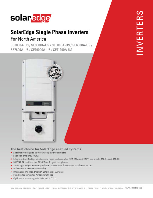
(1) For other regional settings please contact SolarEdge support. (2) A higher current source may be used; the inverter will limit its input current to the values stated. (3) Revenue grade inverter P/N: SExxxxA-US000NNR2 (for 7600W inverter:SE7600A-US002NNR2). (4) -40 version P/N: SExxxxA-US000NNU4 (for 7600W inverter:SE7600A-US002NNU4). (5) P/Ns SExxxxA-US0xxxxxx have Manual Rapid Shutdown for NEC 2014 compliance (NEC 2017 compliance with outdoor installation)
VA VA
Hz A A Yes W Vdc Vdc Adc Adc
% % W
in / mm lb / kg
dBA ˚F / ˚C
© SolarEdge Technologies, Inc. All rights reserved. SOLAREDGE, the SolarEdge logo, OPTIMIZED BY SOLAREDGE are trademarks or registered trademarks of SolarEdge Technologies, Inc. All other trademarks mentioned herein are trademarks of their respective owners. Date: 07/2017. V.01. Subject to change without notice.
KIA50N03规格书

50 Amps, 30 Volts N-CHANNEL MOSFET1.Features⏹ Advanced trench process technology⏹ High density cell design for ultra low on-resistance ⏹ Fully characterized avalanche voltage and current2.Applications⏹ V DSS =30V,R DS(on)=6.5mΩ,I D =50A ⏹ Vds=30V⏹ R DS(ON)=6.5mΩ(Max.),VGS@10V,Ids@30A ⏹ R DS(ON)=9.5mΩ(Max.),VGS@4.5V,Ids@30A3. Pin configurationPin Function 1 Gate 2 Drain 3 Source 4 Drain50N03KIASEMICONDUCTORS4. Maximum ratings and thermal characteristics(T a=25°C,unless otherwise notes)Rating Symbol Value Unit Drain-source voltage V DS30 VGate-source voltage V GS+20 VContinuous drain current I D50 APulsed drain current1)I DM200 AMaximum power dissipation T A=25°C P D60 W T A=75°C P D23 WOperating junction and storage temperature range T J/T STG-55 to 150 °C Junction-to-case thermal resistance RθJC 1.8 °C/W Junction-to ambient themal rasistance (PCB mount)2)RθJA50 °C/WNote:1.Repetitive rating:pulse width limited by the maximum junction temperation2.1-in2 2oz Cu PCB board3.Guaranteed by design;not subject to production testing5. Ordering informationPart number PackageKIA50N03 TO-251,TO-252,TO-2206. Typical application circuit7. Electrical characteristics(T a=25°C,unless otherwise notes) Parameter Symbol T est conditions Min. Typ. Max. Units StaticDrain-source breakdown voltage BV DSS V GS=0V,I D=250μA 30 - - VDrain-source on-state rasistancem R DS(ON)V GS=4.5V,I D=30A - 9.5 13.0 mΩV GS=10V,I D=30A - 6.5 9.0 mΩGate threshold voltage V GS(th)V DS=V GS,I D=-250μA 1 1.8 3 V Forward transconductance g fs V DS=15V,I D=15A - 12 - S Zero gate voltage drain current I DSS V DS=25V,V GS=0V - - 1 μA Gate-source forward leakage I GSS V GS=+20V,V DS=0V - - +100 nA Dynamic3)T otal gate charge Q g ID=35AV DS=15VV GS=10V - 10 25 nCGate-source charge Q gs 3.5 10 nC Gate-drain (“miller”)charge Q gd- 3 65 nCTurn-on delay time t d(off)VDD=15VI D=1AR G=6ΩR L=15ΩV GEN=10V - 12 - nsRise time t r- 4 - ns Turn-off delay time t d(off)- 32 - ns Fall time t f- 6 - nsInput capacitance C issV GS=0VV DS=15Vf=1.0MHz - 1180 - pFOutput capacitance C oss- 270 - pF Reverse transfer capacitance C rss- 145 - pFSource-drain diodeParameter Symbol T est condition Min. Typ. Max. Units Diode forward voltage V SD I S=20A,V GS=0V - 0.87 1.5 V Max.diode forward current I S- - 20 A Notes:Pulse width<300μs,duty cycle<2%。
SUD50N02-06P中文资料

SPICE Device Model SUD50N02-06PVishay SiliconixThis document is intended as a SPICE modeling guideline and does not constitute a commercial product data sheet. Designers should refer to the appropriate data sheet of the same number for guaranteed specification limits.Document Number: 70104 N-Channel 20-V (D-S) 175° MOSFETCHARACTERISTICS• N-Channel Vertical DMOS• Macro Model (Subcircuit Model) • Level 3 MOS• Apply for both Linear and Switching Application • Accurate over the −55 to 125°C Temperature Range• Model the Gate Charge, Transient, and Diode Reverse Recovery CharacteristicsDESCRIPTIONThe attached spice model describes the typical electrical characteristics of the n-channel vertical DMOS. The subcircuit model is extracted and optimized over the −55 to 125°C temperature ranges under the pulsed 0 to 10V gate drive. The saturated output impedance is best fit at the gate bias near the threshold voltage.A novel gate-to-drain feedback capacitance network is used to model the gate charge characteristics while avoiding convergence difficulties of the switched C gd model. All model parameter values are optimized to provide a best fit to the measured electrical data and are not intended as an exact physical interpretation of the device.SUBCIRCUIT MODEL SCHEMATICSPICE Device Model SUD50N02-06P Vishay Siliconix Document Number: 70104SPECIFICATIONS (T J = 25°C UNLESS OTHERWISE NOTED)Parameter Symbol Test ConditionsSimulatedDataMeasured DataUnitStaticGate Threshold Voltage V GS(th) V DS = V GS , I D = 250 µA 1.4 V On-State Drain Current bI D(on)V DS = 5 V, V GS = 10 V 964 AV GS = 10 V, I D = 20 A0.00410.0046V GS = 10 V, I D = 20 A, T J = 125°C0.0057 Drain-Source On-State Resistance br DS(on)V GS = 4.5 V, I D = 20 A0.0065 0.0073 Ω Forward Voltage bV SDI S = 50 A, V GS = 0 V0.911.2VDynamic aInput Capacitance C iss 2418 2550Output CapacitanceC oss 816 900 Reverse Transfer Capacitance C rssV GS = 0 V, V DS = 25 V, f = 1 MHz 348 415pF Total Gate Charge c Q g 20 19Gate-Source Charge c Q gs 7.5 7.5 Gate-Drain Charge c Q gdV DS = 10 V, V GS = 4.5 V, I D = 50 A 6 6nC Turn-On Delay Time c t d(on) 11 11Rise Time ct r 10 10 Turn-Off Delay Time c t d(off) 9 24Fall Time ct f V DD = 10 V, R L = 0.20 Ω I D ≅ 50 A, V GEN = 10 V, R G = 2.5 Ω 9 9 Source-Drain Reverse Recovery Timet rrI F = 50 A, di/dt = 100 A/µs31 35nsNotesa. Guaranteed by design, not subject to production testing.b. Pulse test; pulse width ≤ 300 µs, duty cycle ≤ 2%.c. Independent of operating temperature.SPICE Device Model SUD50N02-06PVishay SiliconixDocument Number: 70104 COMPARISON OF MODEL WITH MEASURED DATA (TJ =25°C UNLESS OTHERWISE NOTED)。
- 1、下载文档前请自行甄别文档内容的完整性,平台不提供额外的编辑、内容补充、找答案等附加服务。
- 2、"仅部分预览"的文档,不可在线预览部分如存在完整性等问题,可反馈申请退款(可完整预览的文档不适用该条件!)。
- 3、如文档侵犯您的权益,请联系客服反馈,我们会尽快为您处理(人工客服工作时间:9:00-18:30)。
FEATURESD TrenchFET r Power MOSFETD Optimized for Low–Side Synchronous Rectifier Operation D 100% R g TestedAPPLICATIONSD DC/DC Converters D Synchronous RectifiersRoHSCOMPLIANTSUD50N03-06APVishay SiliconixNew ProductDocument Number: 73540S–52237—Rev. A, 24-Oct-051N-Channel 30-V (D-S) MOSFETPRODUCT SUMMARYV DS (V)r DS(on) (W )I D (A)a, eQ g(Typ)0.0057 @ V GS = 10 V 90300.0078 @ V GS = 4.5 V7730N-Channel MOSFETGDOrdering Information:SUD50N03-06AP—E3 (Lead (Pb)-free)TO-252SGDTop ViewDrain Connected to TabABSOLUTE MAXIMUM RATINGS (T A = 25_C UNLESS OTHERWISE NOTED)ParameterSymbolLimitUnitDrain-Source Voltage V DS 30Gate-Source VoltageV GS"20VT C = 25_C90a, e Continuous Drain Current 175T C = 70_C 75a, e Continuous Drain Current (T J = 175_C)T A = 25_C I D30b, c T A = 70_C25b, c Pulsed Drain CurrentI DM 100AContinuous Source Drain Diode Current T C = 25_C 55a, e Continuous Source-Drain Diode Current T A = 25_C I S 6.7b, c Avalanche Current Pulse L 01mH I AS 45Single Pulse Avalanche EnergyL = 0.1 mH E AS 101mJ T C = 25_C83Maximum Power Dissipation T C = 70_C 58Maximum Power DissipationT A = 25_C P D 10b, c W T A = 70_C7b, c Operating Junction and Storage Temperature RangeT J , T stg –55 to 175_C THERMAL RESISTANCE RATINGSParameterSymbolTypicalMaximumUnitMaximum Junction-to-Ambient b, d t p 10 sec R thJA 1215Maximum Junction-to-CaseSteady StateR thJC1.51.8_C/WNotes:a.Based on T C = 25_C.b.Surface mounted on 1” x 1” FR4 board.c.t = 10 secd.Maximum under steady state conditions is 50_C/W.e.Calculated based on maximum junction temperature. Package limitation current is 50 A.SUD50N03-06APVishay SiliconixNew Product2Document Number: 73540S–52237—Rev. A, 24-Oct-05SPECIFICATIONS (T J = 25_C UNLESS OTHERWISE NOTED)ParameterSymbol Test Condition Min Typ Max UnitStaticDrain-Source Breakdown Voltage V DS V GS = 0 V, I D = 250 m A30V V DS Temperature Coefficient D V DS /T J I =25025V GS(th) Temperature Coefficient D V GS(th)/T J I D = 250 m A– 6.3mV/_C Gate-Source Threshold Voltage V GS(th)V DS = V GS , I D = 250 m A 1.2 2.4V Gate-Source LeakageI GSS V DS = 0 V, V GS = "20 V "100nA Zero Gate Voltage Drain Current V DS = 30 V, V GS = 0 V 1Zero Gate Voltage Drain Current I DSS V DS = 30 V, V GS = 0 V, T J = 55_C10m A On-State Drain Current aI D(on)V DS w 5 V, V GS = 10 V 50A Drain-Source On-State Resistance V GS = 10 V, I D = 20 A 0.00460.0057Drain-Source On-State Resistance a r DS(on)V GS = 4.5 V, I D = 20 A 0.00620.0078W Forward Transconductance ag fsV DS = 15 V, I D = 30 A70SDynamic bInput Capacitance C iss 3800Output CapacitanceC oss V DS = 15 V, V GS = 0 V, f = 1 MHz615pF Reverse Transfer Capacitance C rss 305pTotal Gate Charge V DS = 15 V, V GS = 10 V, I D = 30 A 6295Total Gate Charge Q g 3045Gate-Source Charge Q gs V DS = 15 V, V GS = 4.5 V, I D = 25 A 11nC Gate-Drain Charge Q gd 9Gate Resistance R g f = 1 MHz0.9 1.4WTurn-On Delay Time t d(on)1218Rise Timet r V 1015Turn-Off Delay Time t d(off)DD = 15 V, R L = 0.5WI D ^ 30 A, V GEN = 10 V, R = 1 W3045Fall Timet f g 812Turn-On Delay Time t d(on)2640ns Rise Timet r V 230345Turn-Off Delay Time t d(off)DD = 15 V, R L =0.6WI D ^ 25 A, V GEN = 4.5 V, R = 1 W 2540Fall Timet fg 914Drain-Source Body Diode CharacteristicsContinuous Source-Drain Diode Current I S T C = 25_C55c Pulse Diode Forward Current a I SM 100A Body Diode VoltageV SD I S = 6.7 A0.9 1.5V Body Diode Reverse Recovery Time t rr 65100ns Body Diode Reverse Recovery Charge Q rr 67A di/dt 100A/s T 25_C3860nC Reverse Recovery Fall Time t a I F = 6.7 A, di/dt = 100 A/m s, T J = 2550Reverse Recovery Rise Timet b15nsNotesa.Pulse test; pulse width v 300 m s, duty cycle v 2%.b.Guaranteed by design, not subject to production testing.c.Calculated based on maximum junction temperature. Package limitation current is 50 A.Stresses beyond those listed under “Absolute Maximum Ratings” may cause permanent damage to the device. These are stress ratings only, and functional operation of the device at these or any other conditions beyond those indicated in the operational sections of the specifications is not implied. Exposure to absolute maximum rating conditions for extended periods may affect device reliability.SUD50N03-06APVishay SiliconixNew ProductDocument Number: 73540S–52237—Rev. A, 24-Oct-0532040608010024681013263952650.70.91.11.31.51.71.9–50–25025507510012515017510002000300040005000510152025Gate ChargeOn-Resistance vs. Drain CurrentQ g (nC)V DS – Drain-to-Source Voltage (V)C – C a p a c i t a n c e (p F )I D – Drain Current (A)CapacitanceOn-Resistance vs. Junction TemperatureT J – Junction Temperaturer D S (o n ) – O n -R e s i s t a n c e (N o r m a l i z e d )0.00.5 1.0 1.5 2.0 2.5 3.0 3.5 4.00.00.5 1.0 1.5 2.0 2.5 3.0V DS – Drain-to-Source Voltage (V)V GS – Gate-to-Source Voltage (V)r D S (o n ) – O n -R e s i s t a n c e (W )V G S (V )SUD50N03-06APVishay SiliconixNew Product4Document Number: 73540S–52237—Rev. A, 24-Oct-05–50–250255075100125150175T J – Temperature (_C)Time (sec)1010000.10.010.0011001Safe Operating Area0.1110100V DS (V)*V GS u minimum V GS at which r DS(on) is specifiedI D (A )11010010000.01SUD50N03-06APVishay SiliconixNew ProductDocument Number: 73540S–52237—Rev. A, 24-Oct-055TYPICAL CHARACTERISTICS (25_C UNLESS NOTED)0255075100255075100125150175Current De-RatingD r a i n C u r r e n t (A )T C – Case Temperature (_C)0102030405060708090255075100125150175Power De-RatingT C – Case Temperature (_C)P o we rSUD50N03-06APVishay SiliconixNew Product6Document Number: 73540S–52237—Rev. A, 24-Oct-05TYPICAL CHARACTERISTICS (25_C UNLESS NOTED)10–310–2110–110–410.1Normalized Thermal Transient Impedance, Junction-to-CaseSquare Wave Pulse Duration (sec)N o r m a l i z e d E f f e c t i v e T r a n s i e n t T h e r m a l I m p e d a n c e1N o r m a l i z e d E f f e c t i v e T r a n s i e n t T h e r m a l I m p e d a n c eVishay Siliconix maintains worldwide manufacturing capability. Products may be manufactured at one of several qualified locations. Reliability data for Silicon T echnology and Package Reliability represent a com posite of all qualified locations. For related docum ents such as package/tape drawings, part m arking, and reliability data, see /ppg?73540.Document Number: 91000Revision: 18-Jul-081DisclaimerLegal Disclaimer NoticeVishayAll product specifications and data are subject to change without notice.Vishay Intertechnology, Inc., its affiliates, agents, and employees, and all persons acting on its or their behalf (collectively, “Vishay”), disclaim any and all liability for any errors, inaccuracies or incompleteness contained herein or in any other disclosure relating to any product.Vishay disclaims any and all liability arising out of the use or application of any product described herein or of any information provided herein to the maximum extent permitted by law. The product specifications do not expand or otherwise modify Vishay’s terms and conditions of purchase, including but not limited to the warranty expressed therein, which apply to these products.No license, express or implied, by estoppel or otherwise, to any intellectual property rights is granted by this document or by any conduct of Vishay.The products shown herein are not designed for use in medical, life-saving, or life-sustaining applications unless otherwise expressly indicated. Customers using or selling Vishay products not expressly indicated for use in such applications do so entirely at their own risk and agree to fully indemnify Vishay for any damages arising or resulting from such use or sale. Please contact authorized Vishay personnel to obtain written terms and conditions regarding products designed for such applications.Product names and markings noted herein may be trademarks of their respective owners.元器件交易网。