V23809-C8-T10中文资料
L298N中文资料

L298N中文资料步进电机驱动芯片L298中文资料双全桥步进电机专用驱动芯片( Dual Full-Bridge Driver )L298中文资料L298N 为SGS-THOMSON Microelectronics 所出产的双全桥步进电机专用驱动芯片( Dual Full-Bridge Driver ) ,内部包含4信道逻辑驱动电路,是一种二相和四相步进电机的专用驱动器,可同时驱动2个二相或1个四相步进电机,内含二个H-Bridge 的高电压、大电流双全桥式驱动器,接收标准TTL逻辑准位信号,可驱动46V、2A以下的步进电机,且可以直接透过电源来调节输出电压;此芯片可直接由单片机的IO端口来提供模拟时序信号,但在本驱动电路中用L297 来提供时序信号,节省了单片机IO 端口的使用。
L298N 之接脚如图9 所示,Pin1 和Pin15 可与电流侦测用电阻连接来控制负载的电路; OUTl、OUT2 和OUT3、OUT4 之间分别接2 个步进电机;input1~input4 输入控制电位来控制电机的正反转;Enable 则控制电机停转。
图9 L298引脚图图10 L298 内部逻辑图L298 ABSOLUTE MAXIMUM RATINGS 绝对最大额定值: Symbol符号Parameter 参数Value数值单位VSPower Supply 电源50VSSLogic Supply Voltage 电源电压7VVI,VenInput and Enable Voltage 输入电压和启用–0.3 to 7VIO峰值输出电流(每通道)非重复性(t= 100ms)3重复(80% on –20% off; ton = 10ms) 2.5直流运行2VsensSensing Voltage 感应电压–1 to 2.3VPtotTotal Power Dissipation (Tcase=75℃)总功率耗散(Tcase=75 ℃)25WTopJunction Operating Temperature 结工作温度–25 to 130℃Tstg,TjStorage and Junction Temperature 储存温度–40 to 150℃L298 PIN FUNCTIONS (refer to the block diagram) 引脚功能(请参阅框图):PowerSONameFunction 功能说明1;152;19Sense A; Sense B 引脚电流监测端,1、15和PowerSO的2、19用法一样,SEN1、SEN2分别为两个H桥的电流反馈脚,不用时可以直接接地2;34;5Out 1; Out 21Y1、1Y2输出端46VS功率电源电压,此引脚与地必须连接100nF电容器 5;77;9Input 1; Input 21A1、1A2输入端,TTL电平兼容6;118;14Enable A; Enable BTTL电平兼容输入 1EN、2EN使能端,低电平禁止输出 81,10,11,20GNDGND地912VSS逻辑电源电压。
Futaba10C-10CH中文说明书(1)

2
目
简介.....................................5 支持与服务............................5 使用、出口和改装......................5 特殊标志的意义........................6 安全注意事项(操作前请务必阅读........6 对 10C 系统的简介.....................8 部件和技术特性.......................11 配件.................................12 发射机控制项和开关设置...............14 对镍镉电池进行充电...................18 操纵杆调整...........................19 调整显示屏的对比度...................19 改变模式.............................20 省电模式(只对 TM10 适用)............20 CP 卡的初始化和数据转换..............20 遥控设备的安装和范围检测.............21 飞行频率.............................26 发射机显示屏和按键...................27 警告和错误显示.......................28
滑翔机的功能菜单........................80 子目录...............................80 从基本的 4 通道滑翔机开始.............81 滑翔机的基础功能菜单.................83 模型类型(PARAMETER 子菜单).........83 电动机关闭 MOTOR CUT................84 滑翔机的高级功能菜单.................85 副翼/方向舵混控 AILE/RUDD............86 副翼,襟翼混控 AILE-FLAP(仅限于滑翔机 [2A+2F]).............................87 阻流板混控 SPOILER MIX................88 微调杆偏置 OFFSETs 附加飞行条件)......89 起飞延迟(仅限于滑翔机[1A+’F[)......90 翼型混控 CAMBER MIX.................90 翼型襟翼 CAMBER FLAP.................91 蝶式混控 BUTTERFLY...................92 通道 3 的功能选择(飞行条件/功能) ( CONDITION/FUNCTION) ...............93
Trigonox 101-SC8B 2,5-Dimethyl-2,5-di(tert-butylpe
产品数据表Trigonox 101-SC8B2,5-Dimethyl-2,5-di(tert-butylperoxy)hexane, gum in silicone rubberCAS 编号78-63-7; 68083-18-1EINECS/ELINCS编号201-128-1; not listedTSCA 状态清单上列出的分子量290.4活性氧含量过氧化物11.02%应用Trigonox® 101-SC8B主要用于硅橡胶的交联。
含有Trigonox® 101-SC8B 的橡胶具有卓越的焦烧安全性。
安全加工温度(流变仪 ts2 > 20 分钟): 135°C。
典型交联温度(流变仪 t90 约 12 分钟): 175°C热稳定性有机过氧化物是热不稳定物质,可发生自加速分解。
自加速分解温度(SADT)是一种物质在其用于运输的包装中可能产生自加速分解的最低温度。
SADT根据热积累储存试验测定。
SADT80°C方法热累积储存试验是公认的用于测定有机过氧化物SADT的测试方法(见《关于危险货物运输的建议书·试验和标准手册》– 联合国,纽约和日内瓦)。
存储由于有机过氧化物的相对不稳定性,随着时间的流逝会有一定的质量损失。
为了使质量损失最小化,诺力昂建议每种有机过氧化物的最高储存温度(最高储存温度)。
最高温度30°C注意当按照所推荐的条件贮存时,Trigonox® 101-SC8B 在交付后至少可在6个月内保持在阿克苏诺贝尔的产品规格范围内。
包装和运输标准的包装是20公升塑料桶装18公斤过氧化物产品。
包装和运输符合国际法规。
关于其它定量包装的可用性,请联系诺力昂公司销售代表。
包装和运输符合国际法规。
关于其它定量包装的可用性,请联系阿克苏诺贝尔公司销售代表。
安全和处理保持容器密闭。
在干燥,通风良好的场所贮存和操作Trigonox® 101-SC8B,远离热源或点火源,避免阳光直晒。
HP ProLiant DL380 Gen9 Server 规格表

Tomorrow’s benchmark for multi-workload compute Purpose-built for flexibility, efficiency, and manageability As the world’s best-selling server,1 the HP ProLiant DL380 Server is designed to adapt to the needs of any environment, from large enterprise to remote office/branch office. With Gen9, the DL380 just got better, offering enhanced reliability, serviceability, and continuous availability, backed by a comprehensive warranty.With the HP ProLiant DL380 Gen9 Server, you can deploy a single platform to handle a wide variety of enterprise workloads:• Virtualization —Consolidate your server footprint by running multiple workloads on a single DL380• Big Data —Manage exponential growth in your data volumes—structured, unstructured, and semi-structured • Storage-centric applications —Remove bottlenecks and improve performance • Data warehousing/analytics —Find the information you need, when you need it, to enable better business decisions • Customer relationship management (CRM)—Gain a 360-degree view of your data to improve customer satisfaction and loyalty • Enterprise resource planning (ERP)—Trust the DL380 Gen9 to help you run your business in near real time • Virtual desktop infrastructure (VDI)—Deploy remote desktop services to provide your workers with the flexibility they need to work anywhere, at any time, using almost any device • SAP ®—Streamline your business processes through consistency and real-time transparency into your end-to-end corporate data To support your heterogeneous IT environment, the DL380 Gen9 Server supports Microsoft ® Windows ® and Linux ® operating systems, as well as VMware ® and Citrix ® virtualization environments.Future-proof design with flexible optionsChoose the features/functions you need now; addmore as necessary as your business needs grow;the modular chassis, networking, and controllerdesigns allow for easy upgrades. Pay for what youneed, when you need it.Industry-leading performance and energyefficiencyFor delivering faster business results and quickerreturns on your investment; Up to 70 percentperformance gain from the Intel ® HaswellE5-2620 v3 processors 2 and ENERGY STAR ®rated systems drive down energy costswith 94 percent 3 efficient power supplies.Agile infrastructure managementFor accelerating IT service delivery; streamlinemanagement with HP OneView 4—therevolutionary converged management platformthat delivers automation simplicity across servers,storage, and networking.Data sheetHP ProLiant DL380 Gen9 ServerThe no-compromise data center standard1 Q114 IDC WW Quarterly Server Tracker, 30thMay 2014.2 I ntel performance testing, comparingmeasurements on platform with two E5-2697 v2(12C, 2.7 GHz), 8x8 GB DDR3-1866, RHEL 6.3 vs.platform with two E5-2697 v3 (14C, 2.6 GHz,145 W), 8x8 GB DDR4-2133, RHEL 6.3, April 2014.3 94 percent efficient (Platinum Plus) HP FlexibleSlot Power Supplies.4 HP OneView support is available for ProLiantGen9 in DL and BL server models only. Expectedavailability is December 2014.Rate this documentSign up for updates /go/getupdated Data sheet | HP ProLiant DL380 Gen9 ServerHP ServicesLet HP help guide you to the New Style of IT. HP Technology Services delivers confidence,reduces risk, and helps you realize greater agility and stability.• Our Consulting services provide advice and guidance to safely move your workloads tonewer technologies.• HP implementation and installation services enable faster, more reliable startup of your newProLiant Gen9 servers, and our support portfolio allows you to get connected and get back tobusiness fast.• We recommend HP Proactive Care for ProLiant Gen9 servers to prevent issues and resolveproblems quickly and efficiently.• HP Foundation Care provides a choice of coverage levels and response times for hardwareand software support.• HP Datacenter Care enables you to operate and evolve your IT environment at a lower costand with more agility, including our Flexible Capacity Service to acquire IT without impactingcapital budget.• Our support technology lets you tap into the knowledge of millions of devices and thousandsof experts to stay informed and in control, anywhere, any time.Learn more at /servers/DL380gen9© Copyright 2014 Hewlett-Packard Development Company, L.P. The information contained herein is subject to change without notice. The onlywarranties for HP products and services are set forth in the express warranty statements accompanying such products and services. Nothing hereinshould be construed as constituting an additional warranty. HP shall not be liable for technical or editorial errors or omissions contained herein.SAP is a registered trademark of SAP AG in Germany and other countries. Microsoft and Windows are U.S. registered trademarks of the Microsoft group ofcompanies. ENERGY STAR is a registered mark owned by the U.S. government. Citrix is a registered trademark of Citrix Systems, Inc. and/or one or more ofits subsidiaries, and may be registered in the United States Patent and Trademark Office and in other countries. Intel and Intel Xeon are trademarks of IntelCorporation in the U.S. and other countries. SD and microSD are trademarks or registered trademarks of SD-3C in the United States, other countries or both.4AA5-4078ENW, September 2014Technical specificationsIn the following table, bold italic text designates a new or improved feature, as compared to the HP ProLiant DL380p Gen8 puteUp to two Intel® Xeon® E5-2600 v3 series, 4/6/8/10/12/14/16/18 cores; PCIe 3.0, up to six available slot(s)MemoryHP SmartMemory (24) DDR4, up to 2,133 MHz (768 GB max)StorageStandard HP Dynamic Smart Array B140i, choice of HP Flexible Smart Array or HP Smart SAS HBA controllers FBWC2 GB DDR3-1,866 MHz, 72-bit wide bus at 14.9 GB/s on P440ar BatteryHP DL/ML/SL 96 W Smart Storage Battery HP SmartDrives24 + 2 SFF/12 + 3 LFF max, HDD/SSD Networking4 x 1GbE Embedded + choice of FlexibleLOM + Standup VGA/serial/USB ports/SDFront VGA opt, rear VGA, and serial standard, 6 USB 3.0, microSD GPU supportSingle-/double-wide and active /passive up to 10.5" (3)On Premise managementHP OneView 5 and HP iLO Advance On Cloud managementHP Insight Online with enhanced mobile app On System managementChanges in HP iLO, HP Smart Update Manager (HP SUM), Intelligent Provisioning and scripting tools; plus the new UEFI and HP RESTful Interface Tool Power and cooling94 percent efficient with Flexible Slot FF Hot plug fans with full N + 1 redundancy, optional high performance fans Industry complianceASHRAE A3 and A4, lower idle power , and ENERGY STAR Power discovery servicesSupported Location discovery servicesOptional Form factor/Chassis depthRack (2U), 26.75" (SFF), 28.75" (LFF)Serviceability—easy install railsStandard Warranty 3/3/3QuickSpecs: /servers/DL380gen9/qs/5HP OneView support is available for ProLiant Gen9 in DL and BL servers expected later in /qref/dl380gen9。
8T10触摸MCU资料
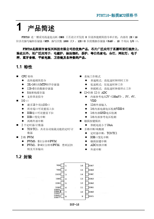
FT8T10-触摸MCU规格书1 产品简述FT8T10 是一颗采用高速低功耗 CMOS 工艺设计开发的 8 位高性能精简指令单片机,内部有2K×16位多次擦写编程存储器(MTP,擦写次数 1000 次),128×8位的数据存储器(RAM),18 个双向 I/O 口,FT8T10是深圳市富恒兴科技有限公司的优势产品,芯片广泛应用于直播环形灯线控上,除此以外,还广泛应用于:电磁炉,抽油烟机,茶炉,等白色家电;台灯,网红灯;电子秤,蓝牙音箱,平板电脑,卫浴镜及各种数码产品。
1.1 特性⏹ CPU 特性● 高性能精简指令● 2K×16位的MTP程序存储器● 128×8位的数据存储器● 8级堆栈缓存器● 支持查表指令⏹ I/O 口● 最多18个双向I/O口● 所有端口可设置弱上拉● IOB端口可设置弱下拉● IOB口变化中断● 两路外部中断⏹ 2 个定时器/计数器● TC0/TC1:具有自动装载功能的定时/计数器⏹ 2 路PWM● PWM0:8位分辨率PWM● PWM1:8+4位分辨率PWM,带死区控制及互补输出⏹ 系统工作模式● 普通模式:高低速时钟同时工作● 低速模式:仅低速时钟工作● 休眠模式:高低速时钟都停止工作⏹ 12+3 路12 位ADC● 内嵌参考电压2V(180mV)、3V、4V、VDD● 12路外部输入● 1路内部电源电压检测VDD/4● 1路内部GND电压检测● 1路内部参考电压检测⏹ 触摸按键模块● 休眠电流小于10uA⏹ 多路中断/唤醒源● 定时器中断:TC0/TC1● IOB口变化中断● 触摸按键中断● ADC转换中断● 外部中断1.2 封装SOP-16。
S108T02;S108T02F;S208T02;中文规格书,Datasheet资料

S108T02 Series S208T02 Series■ FeaturesI T (rms)≤8A, Zero Cross type Low profile SIP 4pin Triac output SSR1. Output current, I T (rms)≤8.0A2. Zero crossing functionary (V OX : MAX. 35V)3. Slim 4 pin low profile SIP package4. High repetitive peak off-state voltage (V DRM : 600V, S208T02 Series ) (V DRM : 400V, S108T02 Series )5. High isolation voltage between input and output (V iso (rms) : 3.0kV)6. Lead-free terminal components are also available (see Model Line-up section in this datasheet)7. Screw hole for heat sink■ DescriptionS108T02 Series and S208T02 Series Solid State Relays (SSR) are an integration of an infrared emitting diode (IRED), a Phototriac Detector and a main output Triac. These devices are ideally suited for controlling high voltage AC loads with solid state reliability while providing 3.0kV isolation (V iso (rms)) from input to out-put.Notice The content of data sheet is subject to change without prior notice.In the absence of confirmation by device specification sheets, SHARP takes no responsibility for any defects that may occur in equipment using any SHARP ■ Agency approvals/Compliance1. Isolated interface between high voltage AC devices and lower voltage DC control circuitry.2. Switching motors, fans, heaters, solenoids, and valves.3. Power control in applications such as lighting and temperature control equipment.■ Applications1. Package resin : UL flammability grade (94V-0)∗Non-zero cross type is also available. (S108T01 Series/S208T01 Series)∗ : Do not allow external connection.( ) : Typical dimensions■ Internal Connection Diagram+)−)■ Outline Dimensions(Unit : mm)Date code (2 digit)Rank markThere is no rank mark indicator and currently there are no rank offered for this device.A.D.199019911992199319941995199619971998199920002001MarkABCDEFHJKLMN Mark P R S T U V W X A B C Mark 123456789O N DMonth January February March April May June July August September October November December A.D 20022003200420052006200720082009201020112012······2nd digitMonth of production 1st digitYear of productionCountry of originJapanrepeats in a 20 year cycle■ Electro-optical CharacteristicsParameter Symbol Unit InputOutput (T a =25˚C)Forward voltageReverse currentRepetitive peak OFF-state currentON-state voltageHolding currentCritical rate of rise of OFF-state voltageCritical rate of rise of OFF-state voltage at commutaion Minimum trigger currentZero cross voltageIsolation resistanceTurn-on time Turn-off timeThermal resistanceV F I R I DRM V T (rms)I H dV/dt (dV/dt)c I FT V OX R ISO t ont off R th (j-c)R th (j-a)I F =20mA V R =3V V D =V DRM I T (rms)=2A, Resistance load, I F =20mA −V D =2/3•V DRM T j =125˚C , V D =2/3•V DRM , dI T /dt =−4.0A/msV D =6V, R L =30ΩI F =8mA DC500V, 40 to 60%RH V D (rms)=100V, AC50Hz, I F =20mAI T (rms)=2A, Resistance load V D (rms)=200V, AC50Hz, I F =20mA I T (rms)=2A, Resistance load V D (rms)=100V, AC50Hz, I F =20mAI T (rms)=2A, Resistance loadV D (rms)=200V, AC50Hz, I F =20mAI T (rms)=2A, Resistance loadBetween junction and case Between junction and ambience Conditions MIN.TYP.MAX.Transfer charac-teristics S108T02S208T02S108T02S208T02−−−−−305−−1010−−−−−−1.2−−−−−−−−−−−−−4.5401.41001001.550−−835−10101010−−V µA µA V mA V/µs V/µs mA V Ωmsms˚C /W ■ Absolute Maximum RatingsParameter Symbol Rating UnitInputOutput(T a =25˚C)Forward current Reverse voltage RMS ON-state current Peak one cycle surge current Repetitive peak OFF-state voltage Non-Repetitive peak OFF-state voltage Critical rate of rise of ON-state current Operating frequency Isolation voltage Operating temperature Storage temperature Soldering temperature *2*1I FV R I T (rms)I surge V DRMV DSMdI T /dt fV iso (rms)T opr T stg T solmA V A A VVA/µs Hz kV ˚C ˚C ˚C*3*3*45068804006004006005045 to 653.0−25 to +100−30 to +125260*1 40 to 60%RH, AC for 1minute, f =60Hz *2 For 10s*3 Refer to Fig.1, Fig.2*4 f =60Hz sine wave, T j =25˚C startS108T02S208T02S108T02S208T02Soldering areaShipping PackageModel No.Sleeve 25pcs/sleeve S108T02F S208T02FI FT [mA](V D =6V, R L =30Ω)MAX.8400MAX.8600V DRM [V]Please contact a local SHARP sales representative to see the actual status of the production.■ Model Line-up (1) (Lead-free terminal components)■ Model Line-up (2) (Lead solder plating components)Shipping PackageModel No.Sleeve 25pcs/sleeve S108T02S208T02I FT [mA](V D =6V, R L =30Ω)MAX.8400MAX.8600V DRM [V]F o r w a r d c u r r e n t I F (m A )Ambient temperature T a (˚C)060−2502550751001255040302010Fig.1 Forward Current vs. AmbientTemperatureFig.2 RMS ON-state Current vs.Ambient TemperatureF o r w a r d c u r r e n t I F (m A )Forward voltage V F (mA)1010.1100Fig.4 Forward Current vs. Forward VoltageFig.3 RMS ON-state Current vs.Case TemperatureR M S O N -s t a t e c u r r e n t I T (r m s )(A )Case temperature T C (°C)010−25255075100125987654321R M S O N -s t a t e c u r r e n t I T (r m s )(A )Ambient temperature T a (˚C)0987654321−25100755025125(1)(2)(3)(4)(5)(1)With infinite heat sink(2)With heat sink (200×200×2mm Al plate)(3)With heat sink (100×100×2mm Al plate)(4)With heat sink (50×50×2mm Al plate)(5)Without heat sink(N ote)In natural cooling condition, please locate Al platevertically, spread the thermal conductive silicone grease on the touch surface of the device and tighten up the device in the center of Al plate at the torque of 0.4N•m.Fig.8-b Repetitive Peak OFF-state Current vs.Ambient Temperature (S208T02)Fig.8-a Repetitive Peak OFF-state Current vs.Ambient Temperature (S108T02)R e p e t i t i v e p e a k O F F -s t a t e c u r r e n t I D R M (A )Ambient temperature T a (˚C)10−910−310−410−510−610−710−8R e p e t i t i v e p e a k O F F -s t a t e c u r r e n t I D R M (A )Ambient temperature T a (˚C)10−910−310−410−510−610−710−8Remarks : Please be aware that all data in the graph are just for reference.Fig.5 Surge Current vs. Power-on CycleFig.6 Minimum Trigger Current vs.Ambient TemperatureFig.7 Maximum ON-state Power Dissipationvs. RMS ON-state CurrentM i n i m u m t r i g g e r c u r r e n t I F T (m A )Ambient temperature T a (°C)0108642S u r g e c u r r e n t I s u r g e (A )Power-on cycle (Times)10080604020120M a x i m u m O N -s t a t e p o w e r d i s s i p a t i o n (W )RMS ON-state current I T (rms)(A)010864297531■ Design ConsiderationsIn order for the SSR to turn off, the triggering current (l F ) must be 0.1mA or less.When the input current (I F ) is below 0.1mA, the output Triac will be in the open circuit mode. However, if the voltage across the Triac, V D , increases faster than rated dV/dt, the Triac may turn on. To avoid this situation, please incorporate a snubber circuit. Due to the many different types of load that can be driven, we can merely recommend some circuit vales to start with : Cs=0.022µF and Rs=47Ω. The operation of the SSR and snubber circuit should be tested and if unintentional switching occurs, please adjust the snubber circuit component values accordingly.When making the transition from On to Off state, a snubber circuit should be used ensure that sudden drops in current are not accompanied by large instantaneous changes in voltage across the Triac.This fast change in voltage is brought about by the phase difference between current and voltage. Primarily, this is experienced in driving loads which are inductive such as motors and solenoids. Following the procedure outlined above should provide sufficient results. For over voltage protection, a Varistor may be used.Any snubber or Varistor used for the above mentioned scenarios should be located as close to the main out-put triac as possible.Particular attention needs to be paid when utilizing SSRs that incorporate zero crossing circuitry.If the phase difference between the voltage and the current at the output pins is large enough, zero crossing type SSRs cannot be used. The result, if zero crossing SSRs are used under this condition, is that the SSR may not turn on and off irregardless of the input current. In this case, only a non zero cross type SSR should be used in combination with the above mentioned snubber circuit selection process.The load current should be within the bounds of derating curve. (Refer to Fig.2) Also, please use the optional heat sink when necessary.In case the optional heat sink is used and the isolation voltage between the device and the optional heat sink is needed, please locate the insulation sheet between the device and the heat sink.When the optional heat sink is equipped, please set up the M3 screw-fastening torque at 0.3 to 0.5N•m.In order to dissipate the heat generated from the inside of device effectively, please follow the below sugges-tions.● Design guide● Recommended Operating ConditionsParameterS108T02S208T02Symbol Unit InputOutputInput signal current at ON state Input signal current at OFF state Load supply voltage Load supply currentFrequencyOperating temperatureI F (ON)I F (OFF)V OUT (rms)I OUT (rms)f T oprmA mA V mA Hz ˚C−−−Locate snubber circuit between output terminals(Cs =0.022µF, Rs =47Ω)−−Conditions(∗) See Fig.2 about derating curve (I T (rms) vs. ambient temperature).16080800.147−20240.1120240I T (rms)×80%(∗)6380MIN.MAX.✩ For additional design assistance, please review our corresponding Optoelectronic Application Notes.● Standard CircuitV +V S108T02● DegradationIn general, the emission of the IRED used in SSR will degrade over time.In the case where long term operation and / or constant extreme temperature fluctuations will be applied to the devices, please allow for a worst case scenario of 50% degradation over 5years.Therefore in order to maintain proper operation, a design implementing these SSRs should provide at least twice the minimum required triggering current from initial operation.(a) Make sure there are no warps or bumps on the heat sink, insulation sheet and device surface.(b) Make sure there are no metal dusts or burrs attached onto the heat sink, insulation sheet and device sur-face.(c) Make sure silicone grease is evenly spread out on the heat sink, insulation sheet and device surface.Silicone grease to be used is as follows;1) There is no aged deterioration within the operating temperature ranges.2) Base oil of grease is hardly separated and is hardly permeated in the device.3) Even if base oil is separated and permeated in the device, it should not degrade the function of a device. Recommended grease : G-746 (Shin-Etsu Chemical Co., Ltd.): G-747 (Shin-Etsu Chemical Co., Ltd.): SC102 (Dow Corning Toray Silicone Co., Ltd.) In case the optional heat sink is screwed up, please solder after screwed.In case of the lead frame bending, please keep the following minimum distance and avoid any mechanical stress between the base of terminals and the molding resin.Some of AC electromagnetic counters or solenoids have built-in rectifier such as the diode.In this case, please use the device carefully since the load current waveform becomes similar with rectangu-lar waveform and this results may not make a device turn off.■ Manufacturing Guidelines● Soldering MethodFlow Soldering (No solder bathing)Flow soldering should be completed below 260˚C and within 10s.Preheating is within the bounds of 100 to 150˚C and 30 to 80s.Please solder within one time.Other noticesPlease test the soldering method in actual condition and make sure the soldering works fine, since the impact on the junction between the device and PCB varies depending on the tooling and soldering conditions.分销商库存信息:SHARP-MICROELECTRONICSS108T02S108T02F S208T02。
2SC3998中文资料(sanyo)中文数据手册「EasyDatasheet - 矽搜」
3.5
3.0 2.5 2.0
集电极1.5耗散,电脑 - 含
1.0
No heatsin k
0.5
0
0
20
40
60
80
100 120 140 160
环境温度,钽 -
°C ITR07886
1.0
7
开关时间5 ,SW时间 -
tf
3 2
0.1
5 7 1.0
2
3
OUTPUT
RL
+ 470μF
200V
IC - VCE
30
7A
6A
5A
24
4A
3A
18
2A
1A 集电极1电2 流,IC - 一个
6
0
IB=0A
0
2
4
6
8
10
集电极 - 发射极电压VCE - V
ITR06226
VCE(SAT) - IC
10
5
3 2
1.0
集电极
-
发射极 5
3 2
饱和电压,VCE(SAT) - V
集电极电流,IC - 一个
ITR06227
IC - VBE
28
24
20
16
12
集电极电流,IC - 一个
8
120°C Ta=
2°5C--°4C0
4
0
0
0.2
0.4
0.6
0.8
1.0
1.2
基极 - 发射极电压,VBE - V
ITR06229
No.2732-2/4
芯片中文手册,看全文,戳
三洋半导体承担所造成的产品使用AT超越,价值观设备故障不承担任何责任即使是瞬间的,额定数值(例如最大额定 值,工作环境范围或其他参数)在产品规格的任何及所有三洋半导体产品上市说明或本文中.
UITRODE公司 U-165 反激式转换器参考设计说明书
UITRODE 公司U-165Lisa DinwoodieReference Design:Isolated 50 Watt Flyback Converter Usingthe UCC3809 Primary Side Controller参考设计:采用UCC3809初级侧控制器的隔离型50W 反激式转换器应用笔记U-165 —— ZHCU009 —— 2001年6月Lisa DinwoodieUITRODE公司U-165-165参考设计:采用UCC3809初级侧控制器的隔离型50W反激式转换器作者:Lisa Dinwoodie摘要对于功率等级为150W(或更低)的单输出或多输出DC-DC转换器而言,反激式功率级是一种普遍的选择。
由于它不像降压型拓扑结构(比如:正激式或推挽式转换器)那样需要使用输出电感器,因此缩减了元件数目和成本。
本应用笔记将评述反激式转换器的功率级和控制电子线路的设计程序。
在这些隔离型转换器中,来自次级侧的误差信号仍需穿越隔离边界以实现稳压。
通过在次级侧上使用具低失调误差放大器的UC3965精密基准(以驱动一个光耦合器)、并在初级侧上采用UCC3809经济型初级侧控制器,实现了一款简单和低成本的50W隔离型电源。
引言本应用笔记所评述的反激式转换器专为与电信行业中所使用的电压范围相对接而设计。
这款5V、50W电源的主要目标是造就一种能够在保持低成本的同时满足所有规格要求的高效设计方案。
该目标是通过在初级侧上使用UCC3809(以提供固定频率电流模式控制)、并在次级侧上采用UC3965的误差放大器和精密基准来实现的。
这些8引脚集成电路均只需极少的外部元件,从而实现了一种经济而有效的设计。
其原理图示于图1中,而材料清单列表于第16页。
1UITRODE 公司U-165U-165APPLICATION NOTED 51N 5819F D Figure 1.Schematic diagram of the –48V to +5V flyback converter.图1:-48V至+5V 反激式转换器的原理示意图2UITRODE 公司U-165-165U-165APPLICATION NOTE3UITRODE公司U-165U-165APPLICATION NOTETheDC transfer function of a CCM flyback con-verter is:V V V V N D D O D IN Rds on +=× (min)()max max ––11(1)where V O equals the output voltage, 5V ,V D =forward voltage drop across rectifier D1,as-sumed to be 0.8V ,V IN = 32 to 72V , V IN(min)= 32V ,V Rds(on)=on voltage drop across MOSFET Q1,equal to R ds(on)x I (primary), assumed to be 1V ,N = turns ratio, equal to N P /N S ,N S = number of transformer secondary turns,N P = number of transformer primary turns,D = duty cycle.Maximum duty cycle,0.45,occurs at minimum in-put voltage.Substituting these values into (1)gives us a turns ratio of 4.66.The turns ratio is inversely proportional to the peak primary current,I PEAK ,but directly proportional to the voltage stress on the switching element.So the peak currents will not become unreasonably high and the voltage stress on the MOSFET will be kept as low as possible,the turns ratio is rounded up only to the next inte-ger value,5,or simply five primary turns for every one secondary turn.Recalculating equation (1)re-sults in an actual D maxof 48%.Switching Frequency Because the magnetic components and filters will be smaller,the tendency is to have as high a switching frequency as possible.Unfortunately,the decision is not quite that clear cut.Core losses,gate charge currents,and switching losses in-crease with higher switching frequencies;peak cur-rents increase with lower switching frequencies.A compromise must be reached between component size,current levels,and acceptable losses.Syn-chronization with other systems and backward compatibility may also be deciding factors.For this design,a fixed frequency (f sw )of 70kHz was cho-sen.At D max equal to 48%,t on(max)becomes 6.9µs.Transformer Design [2]The transformer in a flyback converter is actually a coupled inductor with multiple windings.Trans-formers provide coupling and isolation whereas inductors provide energy storage.The energystored in the air gap of the inductor is equal to:()E L I P PEAK =×22(2)where E is in Joules,L P is the primary inductance in Henries,and I PEAK is the peak primary current in Amperes.When the switch is on,D1(from Figure 2)is reverse biased due to the dot configuration of the transformer.No current flows in the secondary windings and the current in the primary winding ramps up at a rate of:∆∆I t V V L L IN Rds P =(min)(–on)(3)where V IN(min)and V Rds(on)were defined previously and ∆t is equal to t on(max )at V IN(min).The output capacitor,C OUT ,supplies all of the load current at this time.Because the converter is operating in the continuous conduction mode,∆I L is the change in the inductor current which appears as a positive slope ramp on a step.The step is present because there is still current left in the secondary windings when the primary turns on.When the switch turns off,current flows through the secondary winding and D1as a negative ramp on a step,replenishing C OUT and supplying current directly to the load.Based on (3),the primary inductance can be calcu-lated given an acceptable current ripple,I L .For this design,I L was set to equal one-half the peak primary current.For a CCM flyback design,the peak primary current is calculated based upon (4).()I I N D I PEAK OUT L = × +max max –112∆(4)By replacing PEAK ),I OUT(max)with 10A,D max with with 5as detailed earlier,the peak primary current is calculated to be 5.16A and I L calculates to 2.58A.The root mean square,current CCM DC 式中,V O 等于输出电压 (5V),V D = 整流器D1两端的正向压降,假设为0.8V ,V IN = 32V 至72V ,V IN(min) = 32V ,V Rds(on) = MOSFET Q1两端的导通压降,等于R DS(on)×I (primary),假设为1V ,N = 匝数比,等于N P / N S ,N S = 变压器次级匝数,N P = 变压器初级匝数,D = 占空比。
- 1、下载文档前请自行甄别文档内容的完整性,平台不提供额外的编辑、内容补充、找答案等附加服务。
- 2、"仅部分预览"的文档,不可在线预览部分如存在完整性等问题,可反馈申请退款(可完整预览的文档不适用该条件!)。
- 3、如文档侵犯您的权益,请联系客服反馈,我们会尽快为您处理(人工客服工作时间:9:00-18:30)。
*11 dB V23809-C8-T10Multimode 1300 nm LED Fast Ethernet/FDDI/ATM170 MBd 1x9 T ransceiver with ST® Connector•Compliant with Fast Ethernet, FDDI, Fibre Channel,ATM/SONET/SDH standards•Meets mezzanine standard height of 9.8 mm•Compact integrated transceiver unit with duplex SCreceptacle•Single power supply with 3.0 V to 5.5 V range•Extremely low power consumption < 0.7 W at 3.3 V•PECL differential inputs and outputs•System optimized for 62.5/50 µm graded index fiber•Industry standard multisource footprint•T estboard available•UL-94 V-0 certified•ESD Class 2 per MIL-STD 883 Method 3015•Compliant with FCC (Class B) and EN 55022•For distances of up to 2 km on multimode fiberOperating Ambient Temperature (T AMB)............0°C to 85°CStorage Ambient Temperature............................–40°C to 85°CSoldering Conditions, Temp/Time (T SOLD/t SOLD)(MIL-STD 883C, Method 2003)..............................270°C/10sESD Resistance (all pins to V EE, human body)..................1.5 kVOutput Current (I O)...........................................................50 mA*Available also as 8 dB V23809-C8-T11 on requestST® is a registered trademark of AT&TDESCRIPTIONThis data sheet describes the Infineon Fast Ethernet/FDDI/ATM transceiver—part of Infineon Multistandard Transceiver Family. It is fully compliant with the Asynchronous Transfer Mode (ATM) OC-3 standard, the Fiber Distributed Data Interface (FDDI) Low Cost Fiber Physical Layer Medium Dependent (LCF-PMD) draft standard(1), and the FDDI PMD standard(2).ATM was developed because of the need for multimedia appli-cations, including real time transmission. The data rate is scal-able and the ATM protocol is the basis of the broadband public networks being standardized in the International Telegraph and Telephone Consultative Committee (CCITT). ATM can also be used in local private applications.FDDI is a Dual Token Ring standard developed in the U.S. by the Accredited National Standards Committee (ANSC) X3T9, within the Technical Committee X3T9.5. It is applied to the local area networks of stations, transferring data at 100 Mbits/s with a 125MBaud transmission rate. LCF FDDI is specially developed for short distance applications of up to 500m (fiber-to-the-desk) as compared to 2 km for backbone applications.Fast Ethernet was developed because of the higher bandwidth requirement in local area networking. It is based on the proven effectiveness of millions of installed Ethernet systems.The Infineon multimode transceiver is a single unit comprised of a transmitter, a receiver, and an ST receptacle. This design frees the customer from many alignment and PC board layout concerns. The modules are designed for low cost applications. The inputs/outputs are PECL compatible and the unit operates from a 3.0 V to 5.5 V power supply. As an option, the data out-put stages can be switched to static levels during absence of light, as indicated by the Signal Detect function. It can be directly interfaced with available chipsets.Notes1. FDDI Token Ring, Low Cost Fiber Physical Layer Medium Depen-dent (LCF-PMD) ANSI X3T9.5 / 92 LCF-PMD / Proposed Rev. 1.3, September 1, 1992. American National Standard.2. FDDI Token Ring, Physical Layer Medium Dependent (PMD) ANSIX3.166-1990 American National Standard. ISO/IEC 9314-3: 1990. Regulatory Compliance TECHNICAL DATAThe electro-optical characteristics described in the following tables are valid only for use under the recommended operating conditions.Recommended Operating ConditionsNotes1. For V CC–V EE (min., max.). 50% duty cycle. The supply current(I CC2+I CC3) does not include the load drive current (Icc1). Add max.45 mA for the three outputs. Load is 50 Ω into V CC –2V.2. To maintain good LED reliability, the device should not be held in theON state for more than the specified time. Normal operation should be done with 50% duty cycle.3. To achieve proper PECL output levels the 50 Ω termination should bedone to V CC –2 V. For correct termination see the application notes.Feature Standard CommentsElectromagnetic Interference (EMI)FCC Class BEN 55022 Class BCISPR 22Noise frequencyrange:30 MHz to1GHzImmunity: Electrostatic Discharge EN 61000-4-2IEC 1000-4-2Discharges of±15kV with an airdischarge probe onthe receptacle causeno damage.Immunity: Radio Frequency Electromagnetic Field EN 61000-4-3IEC 1000-4-3With a field strengthof 10 V/m rms, noisefrequency rangesfrom 10 MHz to1GHzEye Safety IEC 825-1Class 1Parameter Symbol Min.T yp.Max.Units Ambient Temperature T AMB070°C Power Supply Voltage V CC–V EE3 5.5V Supply Current 3.3 V I CC230mA Supply Current 5 V(1)260T ransmitterData InputHigh VoltageV IH–V CC–1165–880mVData InputLow VoltageV IL–V CC–1810–1475 Threshold Voltage V BB–V CC–1380–1260Input Data Rise/Fall,20%–80%t R, t F0.4 1.3ns Data High Time(2)t on1000 ReceiverOutput Current l O25mA Input Duty CycleDistortiont DCD 1.0nsInput DataDependent Jittert DDjInput Random Jitter t RJ0.76Input CenterWavelengthl C12601380nmElectrical OutputLoad(3)R L50ΩT ransmitter Electro-Optical CharacteristicsNotes1.Measured at the end of 5 meters of 62.5/125/0.275 graded indexfiber using calibrated power meter and a precision test ferrule.Cladding modes are removed. Values valid for EOL and worst-case temperature.2.The input data pattern is a 12.5 MHz square wave pattern.3.Center wavelength is defined as the midpoint between the two50% levels of the optical spectrum of the LED.4.Spectral width (full width, half max) is defined as the differencebetween 50% levels of the optical spectrum of the LED.5.10% to 90% levels. Measured using the 12.5 MHz square wavepattern with an optoelectronic measurement system (detectorand oscilloscope) having 3 dB bandwidth ranging from less than0.1MHz to more than 750 MHz.6.Extinction Ratio is defined as PL/PH x 100%. Measurement systemas in Note 5.7.Optical Power Low is the output power level when a steady statelow data pattern (FDDI Quiet Line state) is used to drive the trans-mitter. Value valid <1 ms after input low.8.Test method as for FDDI-PMD. Jitter values are peak-to-peak.9.Duty Cycle Distortion is defined as 0.5 [(width of wider state) minus(width of narrower state)]. It is measured with stream of IdleSymbols (62.5MHz square wave).10.Measured with the same pattern as for FDDI-PMD.11.Measured with the Halt Line state (12.5 MHz square wave).Receiver Electro-Optical CharacteristicsNotes1.Pattern: Manchester coding / NRZI (no scrambling)2. For a bit error rate (BER) of less than 1x10E–12 over a receiver eyeopening of least 1.5 ns. Measured with a 223–1 PRBS at 155 MBd.3. For a BER of less than 1x10E-12. Measured in the center of the eyeopening with a 223-1 PRBS at 155 MBd.4. Measured at an average optical power level of –20 dBm with a 62.5MHz square wave.5. All jitter values are peak-to-peak. RX output jitter requirements arenot considered in the ATM standard draft. In general the samerequirements as for FDDI are met.6. Measured at an average optical power level of –20 dBm.7. Measured at –33 dBm average power.8. An increase in optical power through the specified level willcause the SIGNAL detect output to switch from a Low state toa High state.9. A decrease in optical power through the specified level willcause the SIGNAL detect output to switch from a High state toa Low state.10. PECL compatible. Load is 50 Ω into V CC –2 V. Measured under DCconditions. For dynamic measurements a tolerance of 50 mV should be added for V CC=5 V.T ransmitter Symbol Min.T yp.Max.Units Data Rate DR170MBaud Launched Power(Average) into 62.5 µmFiber for –C8–C10(1, 2)P O–20–16–14dBmLaunched Power(Average) into 62.5 µmFiber for –C8–C11(1, 2)–22–17Center Wavelength(2, 3)λC12701360nm Spectral Width(FWHM)(2, 4)D l170Output Rise/Fall Time,10%–90%(2, 5)t R, t F0.6 2.5nsTemperatureCoefficient of OpticalOutput PowerTCp0.03dB/°CExtinction Ratio(Dynamic)(2, 6)ER10% Optical Power Low(7)P TD–45dBm Overshoot OS10% Duty CycleDistortion(8, 9)t DCD0.6nsData DependentJitter(8, 10)t DDJ0.3Random Jitter(8, 11)t RJ0.6Receiver Symbol Min.T yp.Max.Units Data Rate DR5(1)170MBaud SensitivityAverage Power)(2)P IN–33–31dBmSensitivity (AveragePower) Center(3)–35.5Saturation (AveragePower)(3)P SAT–14–11Duty CycleDistortion(4, 5)t DCD1nsDeterministicJitter(5, 6)t DJ1Random Jitter(5, 7)t RJSignal DetectAssert Level(8)P SDA–42.5–30dBmSignal DetectDeassert Level(9)P SDD–45–31.5Signal DetectHysteresisP SDA–P SDD1.0dBOutput LowVoltage(10)V OL–V CC–1810–1620mVOutput HighVoltage(10)V OH–V CC–1025–880Output DataRise/Fall Time,20%–80%t R, t F 1.3nsOutput SDRise/Fall Time,20%–80%40Pin Description APPLICATION NOTEThe power supply filtering is required for good EMI perfor-mance. Use short tracks from the inductor L1/L2 to the module V CC-Rx/V CC-Tx.A GND plane under the module is recommended for good EMI and sensitivity performance.Pin Name Level/Logic Pin#DescriptionR x V EE Rx Ground Power Supply1Negative power supply, normally groundRD Rx Output Data PECL Output2Receiver output dataRDn3Inverted receiver output dataRxSD RX Signal Detect PECL Output active high4High level on this output shows there is an optical signal. R x V CC Rx +3.3 V...5 V Power Supply5Positive power supply, +3.3 V...5 VT x V CC Tx +3.3 V...5 V6TxDn Tx Input Data PECL Input7Inverted transmitter input dataTxD8Transmitter input dataT x V EE Tx Ground Power Supply9Negative power supply, normally groundCase Support Not Connected S1/S2Support stud, not connectedAPPLICATION NOTE FOR MULTIMODE 1300 NM LED TRANSCEIVERSolutions for connecting a Infineon 3.3 V Fiber Optic Transceiver to a 5.0 V Framer-/Phy-Device.。