74AC11257DBR中文资料
DM74ALS125MX中文资料

© 2000 Fairchild Semiconductor Corporation DS010620November 1989Revised February 2000DM74ALS125 Quad 3-STATE BufferDM74ALS125Quad 3-STATE BufferGeneral DescriptionThis device contains four independent gates each of which performs a non-inverting buffer function. The outputs have the 3-STATE feature. The 3-STATE circuitry contains a fea-ture that maintains the buffer outputs in 3-STATE (high impedance state) during power supply ramp-up or ramp-down. This eliminates bus glitching problems that arise during power-up and power-down. To minimize the possi-bility that two outputs will attempt to take a common bus to opposite logic levels, the disable time is shorter than the enable time of the outputs.Featuress Advanced low power oxide-isolated ion-implanted Schottky TTL process s Functional and pin compatible with the 74LS counterpart s Switching response specified into 500Ω and 50 pF load s Switching response specifications guaranteed over full temperature and V CC supply range s PNP input design reduces input loading s Low level drive current: 74ALS = 24 mAOrdering Code:Devices also available in T ape and Reel. Specify by appending the suffix letter “X” to the ordering code.Connection Diagram Functional TableY = AH = HIGH Logic Level L = LOW Logic LevelX = Either LOW or HIGH Logic Level Hi-Z = 3-STATE (Outputs are disabled)Logic DiagramOrder Number Package NumberPackage DescriptionDM74ALS125M M14A 14-Lead Small Outline Integrated Circuit (SOIC), JEDEC MS-012, 0.150 Narrow DM74ALS125NN14A14-Lead Plastic Dual-In-Line Package (PDIP), JEDEC MS-001, 0.300 WideInput Output A C Y L L L H L H XHHi-Z 2D M 74A L S 125Absolute Maximum Ratings (Note 1)Note 1: The Absolute Maximum Ratings are those values beyond which the safety of the device cannot be guaranteed. The device should not be operated at these limits. The parametric values defined in the Electrical Characteristics tables are not guaranteed at the absolute maximum ratings.The “Recommended Operating Conditions” table will define the conditions for actual device operation.Recommended Operating ConditionsElectrical Characteristicsover recommended operating free air temperature (unless otherwise specified)Supply Voltage, V CC 7V Input Voltage7V Voltage Applied to Disabled Output 5.5V Operating Free Air Temperature Range 0 to +70°C Storage Temperature Range −65°C to +150°CTypical θJA N Package 78.0°C/W M Package111.0°C/WSymbol ParameterMin Typ Max Units V CC Supply Voltage4.555.5V V IH HIGH Level Input Voltage 2V V IL LOW Level Input Voltage 0.8V I OH HIGH Level Output Current −15mA I OL LOW Level Output Current 24mA T AOperating Free-Air Temperature70°CSymbol ParameterConditionsMinTypMax Units V IK Input Clamp Voltage V CC = 4.5V, I I = −18 mA −1.5V V OHHIGH Level V CC = 4.5V to 5.5V I OH = −0.4 mA V CC −2V Output VoltageV CC = 4.5V I OH = −3 mA 2.4V I OH = Max 2V V OL LOW Level V CC = 4.5VI OL = 12 mA 0.250.4V Output Voltage I OL = 24 mA0.350.5V I I Input Current at Max V CC = 5.5V, V I = 7V 0.1mA Input Voltage I IH HIGH Level V CC = 5.5V, V I = 2.7V 20µA Input Current I IL LOW Level V CC = 5.5V, V IL = 0.4V −0.1mA Input Current I O Output Drive V CC = 5.5V, V O = 2.25V −30−112mA CurrentI OZH HIGH Level 3-STATE V CC = 5.5V, V O = 2.7V 20µA Output Current I OZL LOW Level 3-STATE V CC = 5.5V, V O = 0.4V −20µA Output Current I CCSupply CurrentV CC = 5.5VOutputs HIGH 710mA Outputs LOW 1014mA 3-STATE13.518mADM74ALS125Switching CharacteristicsSymbol ParameterFrom To Conditions Min MaxUnits (Input)(Output)t PLH Propagation Delay Time A Y V CC = 4.5V to 5.5V,310ns LOW-to-HIGH Level Output C L = 50 pF,t PHL Propagation Delay Time A Y R1 = 500Ω,210ns HIGH-to-LOW Level Output R2 = 500Ω,t PZH Output Enable Time C Y T A = Min to Max213ns to HIGH Level Output t PZL Output Enable Time C Y 212ns to LOW Level Output t PHZ Output Disable Time C Y 18ns from HIGH Level Output t PLZOutput Disable Time CY213nsfrom LOW Level Output 4D M 74A L S 125Physical Dimensionsinches (millimeters) unless otherwise noted14-Lead Small Outline Integrated Circuit (SOIC), JEDEC MS-012, 0.150 NarrowPackage Number M14A5DM74ALS125 Quad 3-STATE BufferPhysical Dimensions inches (millimeters) unless otherwise noted (Continued)14-Lead Plastic Dual-In-Line Package (PDIP), JEDEC MS-001, 0.300 WidePackage Number N14AFairchild does not assume any responsibility for use of any circuitry described, no circuit patent licenses are implied and Fairchild reserves the right at any time without notice to change said circuitry and specifications.LIFE SUPPORT POLICYFAIRCHILD’S PRODUCTS ARE NOT AUTHORIZED FOR USE AS CRITICAL COMPONENTS IN LIFE SUPPORT DEVICES OR SYSTEMS WITHOUT THE EXPRESS WRITTEN APPROVAL OF THE PRESIDENT OF FAIRCHILD SEMICONDUCTOR CORPORATION. As used herein:1.Life support devices or systems are devices or systems which, (a) are intended for surgical implant into the body, or (b) support or sustain life, and (c) whose failure to perform when properly used in accordance with instructions for use provided in the labeling, can be rea-sonably expected to result in a significant injury to the user.2. A critical component in any component of a life support device or system whose failure to perform can be rea-sonably expected to cause the failure of the life support device or system, or to affect its safety or effectiveness.。
74系列芯片标准数字电路资料

74系列芯片标准数字电路资料-功能大全一.74系列芯片标准数字电路资料-功能大全二。
74系列芯片资料三.74HC/LS/HCT/F系列芯片的区别四.逻辑电平介绍TTL,CMOS五.74HC244与245作用与区别六.74芯片分类总汇一.74系列芯片标准数字电路资料-功能大全7400 TTL 2输入端四与非门7401 TTL 集电极开路2输入端四与非门7402 TTL 2输入端四或非门7403 TTL 集电极开路2输入端四与非门7404 TTL 六反相器7405 TTL 集电极开路六反相器7406 TTL 集电极开路六反相高压驱动器7407 TTL 集电极开路六正相高压驱动器7408 TTL 2输入端四与门7409 TTL 集电极开路2输入端四与门7410 TTL 3输入端3与非门74107 TTL 带清除主从双J-K触发器74109 TTL 带预置清除正触发双J-K触发器7411 TTL 3输入端3与门74112 TTL 带预置清除负触发双J-K触发器7412 TTL 开路输出3输入端三与非门74121 TTL 单稳态多谐振荡器74122 TTL 可再触发单稳态多谐振荡器74123 TTL 双可再触发单稳态多谐振荡器74125 TTL 三态输出高有效四总线缓冲门74126 TTL 三态输出低有效四总线缓冲门7413 TTL 4输入端双与非施密特触发器74132 TTL 2输入端四与非施密特触发器74133 TTL 13输入端与非门74136 TTL 四异或门74138 TTL 3-8线译码器/复工器74139 TTL 双2-4线译码器/复工器7414 TTL 六反相施密特触发器74145 TTL BCD—十进制译码/驱动器7415 TTL 开路输出3输入端三与门74150 TTL 16选1数据选择/多路开关74151 TTL 8选1数据选择器74153 TTL 双4选1数据选择器74154 TTL 4线—16线译码器74155 TTL 图腾柱输出译码器/分配器74156 TTL 开路输出译码器/分配器74157 TTL 同相输出四2选1数据选择器74158 TTL 反相输出四2选1数据选择器7416 TTL 开路输出六反相缓冲/驱动器74160 TTL 可预置BCD异步清除计数器74161 TTL 可予制四位二进制异步清除计数器74162 TTL 可预置BCD同步清除计数器74163 TTL 可予制四位二进制同步清除计数器74164 TTL 八位串行入/并行输出移位寄存器74165 TTL 八位并行入/串行输出移位寄存器74166 TTL 八位并入/串出移位寄存器74169 TTL 二进制四位加/减同步计数器7417 TTL 开路输出六同相缓冲/驱动器74170 TTL 开路输出4×4寄存器堆74173 TTL 三态输出四位D型寄存器74174 TTL 带公共时钟和复位六D触发器74175 TTL 带公共时钟和复位四D触发器74180 TTL 9位奇数/偶数发生器/校验器74181 TTL 算术逻辑单元/函数发生器74185 TTL 二进制—BCD代码转换器74190 TTL BCD同步加/减计数器74191 TTL 二进制同步可逆计数器74192 TTL 可预置BCD双时钟可逆计数器74193 TTL 可预置四位二进制双时钟可逆计数器74194 TTL 四位双向通用移位寄存器74195 TTL 四位并行通道移位寄存器74196 TTL 十进制/二-十进制可预置计数锁存器74197 TTL 二进制可预置锁存器/计数器7420 TTL 4输入端双与非门7421 TTL 4输入端双与门7422 TTL 开路输出4输入端双与非门74221 TTL 双/单稳态多谐振荡器74240 TTL 八反相三态缓冲器/线驱动器74241 TTL 八同相三态缓冲器/线驱动器74243 TTL 四同相三态总线收发器74244 TTL 八同相三态缓冲器/线驱动器74245 TTL 八同相三态总线收发器74247 TTL BCD—7段15V输出译码/驱动器74248 TTL BCD—7段译码/升压输出驱动器74249 TTL BCD—7段译码/开路输出驱动器74251 TTL 三态输出8选1数据选择器/复工器74253 TTL 三态输出双4选1数据选择器/复工器74256 TTL 双四位可寻址锁存器74257 TTL 三态原码四2选1数据选择器/复工器74258 TTL 三态反码四2选1数据选择器/复工器74259 TTL 八位可寻址锁存器/3-8线译码器7426 TTL 2输入端高压接口四与非门74260 TTL 5输入端双或非门74266 TTL 2输入端四异或非门7427 TTL 3输入端三或非门74273 TTL 带公共时钟复位八D触发器74279 TTL 四图腾柱输出S-R锁存器7428 TTL 2输入端四或非门缓冲器74283 TTL 4位二进制全加器74290 TTL 二/五分频十进制计数器74293 TTL 二/八分频四位二进制计数器74295 TTL 四位双向通用移位寄存器74298 TTL 四2输入多路带存贮开关74299 TTL 三态输出八位通用移位寄存器7430 TTL 8输入端与非门7432 TTL 2输入端四或门74322 TTL 带符号扩展端八位移位寄存器74323 TTL 三态输出八位双向移位/存贮寄存器7433 TTL 开路输出2输入端四或非缓冲器74347 TTL BCD—7段译码器/驱动器74352 TTL 双4选1数据选择器/复工器74353 TTL 三态输出双4选1数据选择器/复工器74365 TTL 门使能输入三态输出六同相线驱动器74365 TTL 门使能输入三态输出六同相线驱动器74366 TTL 门使能输入三态输出六反相线驱动器74367 TTL 4/2线使能输入三态六同相线驱动器74368 TTL 4/2线使能输入三态六反相线驱动器7437 TTL 开路输出2输入端四与非缓冲器74373 TTL 三态同相八D锁存器74374 TTL 三态反相八D锁存器74375 TTL 4位双稳态锁存器74377 TTL 单边输出公共使能八D锁存器74378 TTL 单边输出公共使能六D锁存器74379 TTL 双边输出公共使能四D锁存器7438 TTL 开路输出2输入端四与非缓冲器74380 TTL 多功能八进制寄存器7439 TTL 开路输出2输入端四与非缓冲器74390 TTL 双十进制计数器74393 TTL 双四位二进制计数器7440 TTL 4输入端双与非缓冲器7442 TTL BCD—十进制代码转换器74352 TTL 双4选1数据选择器/复工器74353 TTL 三态输出双4选1数据选择器/复工器74365 TTL 门使能输入三态输出六同相线驱动器74366 TTL 门使能输入三态输出六反相线驱动器74367 TTL 4/2线使能输入三态六同相线驱动器74368 TTL 4/2线使能输入三态六反相线驱动器7437 TTL 开路输出2输入端四与非缓冲器74373 TTL 三态同相八D锁存器74374 TTL 三态反相八D锁存器74375 TTL 4位双稳态锁存器74377 TTL 单边输出公共使能八D锁存器74378 TTL 单边输出公共使能六D锁存器74379 TTL 双边输出公共使能四D锁存器7438 TTL 开路输出2输入端四与非缓冲器74380 TTL 多功能八进制寄存器7439 TTL 开路输出2输入端四与非缓冲器74390 TTL 双十进制计数器74393 TTL 双四位二进制计数器7440 TTL 4输入端双与非缓冲器7442 TTL BCD—十进制代码转换器74447 TTL BCD—7段译码器/驱动器7445 TTL BCD—十进制代码转换/驱动器74450 TTL 16:1多路转接复用器多工器74451 TTL 双8:1多路转接复用器多工器74453 TTL 四4:1多路转接复用器多工器7446 TTL BCD—7段低有效译码/驱动器74460 TTL 十位比较器74461 TTL 八进制计数器74465 TTL 三态同相2与使能端八总线缓冲器74466 TTL 三态反相2与使能八总线缓冲器74467 TTL 三态同相2使能端八总线缓冲器74468 TTL 三态反相2使能端八总线缓冲器74469 TTL 八位双向计数器7447 TTL BCD—7段高有效译码/驱动器7448 TTL BCD—7段译码器/内部上拉输出驱动74490 TTL 双十进制计数器74491 TTL 十位计数器74498 TTL 八进制移位寄存器7450 TTL 2-3/2-2输入端双与或非门74502 TTL 八位逐次逼近寄存器74503 TTL 八位逐次逼近寄存器7451 TTL 2-3/2-2输入端双与或非门74533 TTL 三态反相八D锁存器74534 TTL 三态反相八D锁存器7454 TTL 四路输入与或非门74540 TTL 八位三态反相输出总线缓冲器7455 TTL 4输入端二路输入与或非门74563 TTL 八位三态反相输出触发器74564 TTL 八位三态反相输出D触发器74573 TTL 八位三态输出触发器74574 TTL 八位三态输出D触发器74645 TTL 三态输出八同相总线传送接收器74670 TTL 三态输出4×4寄存器堆7473 TTL 带清除负触发双J-K触发器7474 TTL 带置位复位正触发双D触发器7476 TTL 带预置清除双J-K触发器7483 TTL 四位二进制快速进位全加器7485 TTL 四位数字比较器7486 TTL 2输入端四异或门7490 TTL 可二/五分频十进制计数器7493 TTL 可二/八分频二进制计数器7495 TTL 四位并行输入\\输出移位寄存器7497 TTL 6位同步二进制乘法器二。
HD74ALVC2G125US中文资料

Rev.0, Jul. 2001, page 2 of 13
HD74ALVC2G125
Pin Arrangement
OE1
1
8
VCC
A1
2
7
OE2
Y2
3
6
Y1
GND
4
5
A2
(Top view)
Absolute Maximum Ratings
Item Supply voltage range Input voltage range
Rev.0, Jul. 2001, page 3 of 13
HD74ALVC2G125
Recommended Operating Conditions
Item Supply voltage range Input voltage range Output voltage range Output current Symbol VCC VI VO IOH Min 1.2 0 0 IOL Input transition rise or fall rate ∆t / ∆v Ta 0 0 Operating free-air temperature −40 Note: Unused or floating inputs must be held high or low. Max 3.6 3.6 VCC −2 −4 −6 −18 −24 2 4 6 18 24 20 10 85 °C ns / V Unit V V V mA VCC = 1.2 V VCC = 1.4 V VCC = 1.65 V VCC = 2.3 V VCC = 3.0 V VCC = 1.2 V VCC = 1.4 V VCC = 1.65 V VCC = 2.3 V VCC = 3.0 V VCC = 1.2 to 2.7 V VCC = 3.3±0.3 V Conditions
74HC1G125GW-R中文资料

4. Ordering information
Table 2: Ordering information
Type number
Package
Temperature range Name
74HC1G125
74HC1G125GW −40 °C to +125 °C TSSOP5
74HC1G125GV 74HCT1G125 74HCT1G125GW
VCC VI VO Tamb tr, tf
supply voltage input voltage output voltage ambient temperature input rise and fall times
VCC = 4.5 V
Min Typ Max Unit
2.0 5.0 6.0 V
74HC1G125; 74HCT1G125
Bus buffer/line driver; 3-state
8. Functional description
8.1 Function table
Table 5: Control OE L L H
Function table [1]
Input A L H X
3. Quick reference data
Table 1: Quick reference data GND = 0 V; Tamb = 25 °C; tr = tf ≤ 6.0 ns.
Symbol Parameter
Conditions
74HC1G125
tPHL, tPLH
Ci
propagation delay A to Y VCC = 5 V; CL = 15 pF input capacitance
74系列各个芯片详细介绍
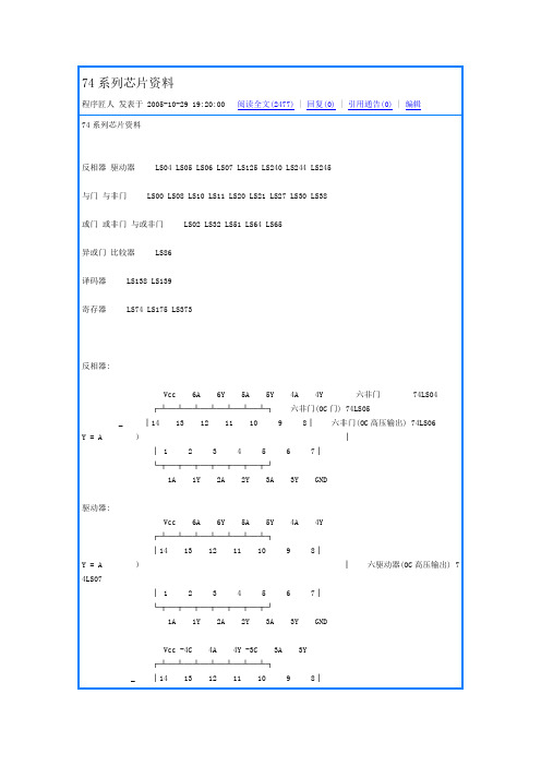
74系列芯片资料程序匠人发表于 2005-10-29 19:20:00 阅读全文(2477) | 回复(0) | 引用通告(0) | 编辑74系列芯片资料反相器驱动器 LS04 LS05 LS06 LS07 LS125 LS240 LS244 LS245与门与非门 LS00 LS08 LS10 LS11 LS20 LS21 LS27 LS30 LS38或门或非门与或非门 LS02 LS32 LS51 LS64 LS65异或门比较器 LS86译码器 LS138 LS139寄存器 LS74 LS175 LS373反相器:Vcc 6A 6Y 5A 5Y 4A 4Y 六非门 74LS04┌┴─┴─┴─┴─┴─┴─┴┐六非门(OC门) 74LS05_ │14 13 12 11 10 9 8│六非门(OC高压输出) 74LS06Y = A )││ 1 2 3 4 5 6 7│└┬─┬─┬─┬─┬─┬─┬┘1A 1Y 2A 2Y 3A 3Y GND驱动器:Vcc 6A 6Y 5A 5Y 4A 4Y┌┴─┴─┴─┴─┴─┴─┴┐│14 13 12 11 10 9 8│Y = A )│六驱动器(OC高压输出) 74LS07│ 1 2 3 4 5 6 7│└┬─┬─┬─┬─┬─┬─┬┘1A 1Y 2A 2Y 3A 3Y GNDVcc -4C 4A 4Y -3C 3A 3Y┌┴─┴─┴─┴─┴─┴─┴┐_ │14 13 12 11 10 9 8│Y =A+C )│四总线三态门 74LS125│ 1 2 3 4 5 6 7│└┬─┬─┬─┬─┬─┬─┬┘-1C 1A 1Y -2C 2A 2Y GNDVcc -G B1 B2 B3 B4 B8 B6 B7 B8┌┴─┴─┴─┴─┴─┴─┴─┴─┴─┴┐ 8位总线驱动器 74LS245 │20 19 18 17 16 15 14 13 12 11│)│ DIR=1 A=>B│ 1 2 3 4 5 6 7 8 9 10│ DIR=0 B=>A└┬─┬─┬─┬─┬─┬─┬─┬─┬─┬┘DIR A1 A2 A3 A4 A5 A6 A7 A8 GND页首非门,驱动器与门,与非门或门,或非门异或门,比较器译码器寄存器正逻辑与门,与非门:Vcc 4B 4A 4Y 3B 3A 3Y┌┴─┴─┴─┴─┴─┴─┴┐│14 13 12 11 10 9 8│Y = AB )│ 2输入四正与门 74LS08 │ 1 2 3 4 5 6 7│└┬─┬─┬─┬─┬─┬─┬┘1A 1B 1Y 2A 2B 2Y GNDVcc 4B 4A 4Y 3B 3A 3Y┌┴─┴─┴─┴─┴─┴─┴┐__ │14 13 12 11 10 9 8│Y = AB )│ 2输入四正与非门 74LS00 │ 1 2 3 4 5 6 7│└┬─┬─┬─┬─┬─┬─┬┘1A 1B 1Y 2A 2B 2Y GNDVcc 1C 1Y 3C 3B 3A 3Y┌┴─┴─┴─┴─┴─┴─┴┐___ │14 13 12 11 10 9 8│Y = ABC )│ 3输入三正与非门 74LS10 │ 1 2 3 4 5 6 7│└┬─┬─┬─┬─┬─┬─┬┘1A 1B 2A 2B 2C 2Y GNDVcc H G Y┌┴─┴─┴─┴─┴─┴─┴┐│14 13 12 11 10 9 8│)│ 8输入与非门 74LS30│ 1 2 3 4 5 6 7│ ________└┬─┬─┬─┬─┬─┬─┬┘ Y = ABCDEFGHA B C D E F GND页首非门,驱动器与门,与非门或门,或非门异或门,比较器译码器寄存器正逻辑或门,或非门:Vcc 4B 4A 4Y 3B 3A 3Y┌┴─┴─┴─┴─┴─┴─┴┐ 2输入四或门 74LS32│14 13 12 11 10 9 8│)│ Y = A+B│ 1 2 3 4 5 6 7│└┬─┬─┬─┬─┬─┬─┬┘1A 1B 1Y 2A 2B 2Y GNDVcc 4Y 4B 4A 3Y 3B 3A┌┴─┴─┴─┴─┴─┴─┴┐ 2输入四或非门 74LS02│14 13 12 11 10 9 8│ ___)│ Y = A+B│ 1 2 3 4 5 6 7│└┬─┬─┬─┬─┬─┬─┬┘1Y 1A 1B 2Y 2A 2B GNDVcc 2Y 2B 2A 2D 2E 1F┌┴─┴─┴─┴─┴─┴─┴┐双与或非门 74S51│14 13 12 11 10 9 8│ _____)│ 2Y = AB+DE│ 1 2 3 4 5 6 7│ _______└┬─┬─┬─┬─┬─┬─┬┘ 1Y = ABC+DEF1Y 1A 1B 1C 1D 1E GNDVcc D C B K J Y┌┴─┴─┴─┴─┴─┴─┴┐ 4-2-3-2与或非门 74S64 74S65(OC门) │14 13 12 11 10 9 8│ ______________)│ Y = ABCD+EF+GHI+JK│ 1 2 3 4 5 6 7│└┬─┬─┬─┬─┬─┬─┬┘A E F G H I GND页首非门,驱动器与门,与非门或门,或非门异或门,比较器译码器寄存器2输入四异或门 74LS86Vcc 4B 4A 4Y 3Y 3B 3A┌┴─┴─┴─┴─┴─┴─┴┐│14 13 12 11 10 9 8│)│ _ _│ 1 2 3 4 5 6 7│ Y=AB+AB└┬─┬─┬─┬─┬─┬─┬┘1A 1B 1Y 2Y 2A 2B GND8*2输入比较器 74LS688_Vcc Y B8 A8 B7 A7 B6 A6 B5 A5┌┴─┴─┴─┴─┴─┴─┴─┴─┴─┴┐ 8*2输入比较器 74LS688│20 19 18 17 16 15 14 13 12 11│)││ 1 2 3 4 5 6 7 8 9 10│└┬─┬─┬─┬─┬─┬─┬─┬─┬─┬┘CE A1 B1 A2 B2 A3 B3 A4 B4 GND_Y=A1⊙B1+A2⊙B2+A3⊙B3+A4⊙B4+A5⊙B5+A6⊙B6+A7⊙B7+A8⊙B8页首非门,驱动器与门,与非门或门,或非门异或门,比较器译码器寄存器3-8译码器 74LS138Vcc -Y0 -Y1 -Y2 -Y3 -Y4 -Y5 -Y6 __ _ _ _ __ _ _ __ _ _ __ _ ┌┴─┴─┴─┴─┴─┴─┴─┴┐ Y0=A B C Y1=A B B Y2=A B C Y3=A B C │16 15 14 13 12 11 10 9 │)│ __ _ _ __ _ __ _ __│ 1 2 3 4 5 6 7 8│ Y4=A B C Y5=A B C Y6=A B C Y7=A B C └┬─┬─┬─┬─┬─┬─┬─┬┘A B C -CS0 -CS1 CS2 -Y7 GND双2-4译码器 74LS139Vcc -2G 2A 2B -Y0 -Y1 -Y2 -Y3 __ __ __ __ __ __ __ __┌┴─┴─┴─┴─┴─┴─┴─┴┐ Y0=2A 2B Y1=2A 2B Y2=2A 2B Y3=2A 2B │16 15 14 13 12 11 10 9 │)│ __ __ __ __ __ __ __ __│ 1 2 3 4 5 6 7 8│ Y0=1A 1B Y1=1A 1B Y2=1A 1B Y3=1A 1B └┬─┬─┬─┬─┬─┬─┬─┬┘-1G 1A 1B -Y0 -Y1 -Y2 -Y3 GND8*2输入比较器 74LS688_Vcc Y B8 A8 B7 A7 B6 A6 B5 A5┌┴─┴─┴─┴─┴─┴─┴─┴─┴─┴┐ 8*2输入比较器 74LS688│20 19 18 17 16 15 14 13 12 11│)││ 1 2 3 4 5 6 7 8 9 10│└┬─┬─┬─┬─┬─┬─┬─┬─┬─┬┘CE A1 B1 A2 B2 A3 B3 A4 B4 GND_Y=A1⊙B1+A2⊙B2+A3⊙B3+A4⊙B4+A5⊙B5+A6⊙B6+A7⊙B7+A8⊙B8寄存器:Vcc 2CR 2D 2Ck 2St 2Q -2Q┌┴─┴─┴─┴─┴─┴─┴┐双D触发器 74LS74│14 13 12 11 10 9 8 │)││ 1 2 3 4 5 6 7│└┬─┬─┬─┬─┬─┬─┬┘1Cr 1D 1Ck 1St 1Q -1Q GNDVcc 8Q 8D 7D 7Q 6Q 6D 5D 5Q ALE┌┴─┴─┴─┴─┴─┴─┴─┴─┴─┴┐ 8位锁存器 74LS373│20 19 18 17 16 15 14 13 12 11│)││ 1 2 3 4 5 6 7 8 9 10│└┬─┬─┬─┬─┬─┬─┬─┬─┬─┬┘-OE 1Q 1D 2D 2Q 3Q 3D 4D 4Q GND型号器件名称厂牌[数据表]SN7400四2输入端与非门 TI[DATA]SN7401四2输入端与非门(OC) SN7402四2输入端或非门 TI[DATA]SN7403四2输入端与非门(OC)TI[DATA]SN7404六反相器 TI[DATA]SN7405六反相器(OC)TI[DATA]SN7406六高压输出反相器 (OC,30V)TI[DATA]SN7407六高压输出缓冲,驱动器(OC,30V)TI[DATA]SN7408四2输入端与门 TI[DATA]SN7409四2输入端与门(OC)TI[DATA]SN7410三3输入端与非门 TI[DATA]SN7412三3输入端与非门(OC)TI[DATA]SN7413双4输入端与非门 TI[DATA]SN7414六反相器TI[DATA]SN7416六高压输出反相缓冲/驱动器 I[DATA]SN7417六高压输出缓冲/驱动器(OC,15V)TI[DATA]SN7420双4输入端与非门 TI[DATA]SN7422双4输入端与非门(OC)TI[DATA]SN7423可扩展双4输入端或非门 TI[DATA]SN7425双4输入端或非门TI[DATA]SN7426四2输入端高压输出与非缓冲器 [DATA]SN7427三3输入端或非门TI[DATA]SN7428四2输入端或非缓冲器 I[DATA]SN74308输入端与非门TI[DATA]SN7432四2输入端或门。
SN74AHC1G125_07中文资料

PACKAGING INFORMATIONOrderable Device Status(1)PackageType PackageDrawingPins PackageQtyEco Plan(2)Lead/Ball Finish MSL Peak Temp(3)74AHC1G125DBVRE4ACTIVE SOT-23DBV53000Green(RoHS&no Sb/Br)CU NIPDAU Level-1-260C-UNLIM74AHC1G125DBVRG4ACTIVE SOT-23DBV53000Green(RoHS&no Sb/Br)CU NIPDAU Level-1-260C-UNLIM74AHC1G125DBVTE4ACTIVE SOT-23DBV5250Green(RoHS&no Sb/Br)CU NIPDAU Level-1-260C-UNLIM74AHC1G125DBVTG4ACTIVE SOT-23DBV5250Green(RoHS&no Sb/Br)CU NIPDAU Level-1-260C-UNLIM74AHC1G125DCKRE4ACTIVE SC70DCK53000Green(RoHS&no Sb/Br)CU NIPDAU Level-1-260C-UNLIM74AHC1G125DCKRG4ACTIVE SC70DCK53000Green(RoHS&no Sb/Br)CU NIPDAU Level-1-260C-UNLIM74AHC1G125DCKTE4ACTIVE SC70DCK5250Green(RoHS&no Sb/Br)CU NIPDAU Level-1-260C-UNLIM74AHC1G125DCKTG4ACTIVE SC70DCK5250Green(RoHS&no Sb/Br)CU NIPDAU Level-1-260C-UNLIM74AHC1G125DRLRG4ACTIVE SOT DRL54000Green(RoHS&no Sb/Br)CU NIPDAU Level-1-260C-UNLIMSN74AHC1G125DBVR ACTIVE SOT-23DBV53000Green(RoHS&no Sb/Br)CU NIPDAU Level-1-260C-UNLIMSN74AHC1G125DBVT ACTIVE SOT-23DBV5250Green(RoHS&no Sb/Br)CU NIPDAU Level-1-260C-UNLIMSN74AHC1G125DCKR ACTIVE SC70DCK53000Green(RoHS&no Sb/Br)CU NIPDAU Level-1-260C-UNLIMSN74AHC1G125DCKT ACTIVE SC70DCK5250Green(RoHS&no Sb/Br)CU NIPDAU Level-1-260C-UNLIMSN74AHC1G125DRLR ACTIVE SOT DRL54000Green(RoHS&no Sb/Br)CU NIPDAU Level-1-260C-UNLIM(1)The marketing status values are defined as follows:ACTIVE:Product device recommended for new designs.LIFEBUY:TI has announced that the device will be discontinued,and a lifetime-buy period is in effect.NRND:Not recommended for new designs.Device is in production to support existing customers,but TI does not recommend using this part in a new design.PREVIEW:Device has been announced but is not in production.Samples may or may not be available.OBSOLETE:TI has discontinued the production of the device.(2)Eco Plan-The planned eco-friendly classification:Pb-Free(RoHS),Pb-Free(RoHS Exempt),or Green(RoHS&no Sb/Br)-please check /productcontent for the latest availability information and additional product content details.TBD:The Pb-Free/Green conversion plan has not been defined.Pb-Free(RoHS):TI's terms"Lead-Free"or"Pb-Free"mean semiconductor products that are compatible with the current RoHS requirements for all6substances,including the requirement that lead not exceed0.1%by weight in homogeneous materials.Where designed to be soldered at high temperatures,TI Pb-Free products are suitable for use in specified lead-free processes.Pb-Free(RoHS Exempt):This component has a RoHS exemption for either1)lead-based flip-chip solder bumps used between the die and package,or2)lead-based die adhesive used between the die and leadframe.The component is otherwise considered Pb-Free(RoHS compatible)as defined above.Green(RoHS&no Sb/Br):TI defines"Green"to mean Pb-Free(RoHS compatible),and free of Bromine(Br)and Antimony(Sb)based flame retardants(Br or Sb do not exceed0.1%by weight in homogeneous material)(3)MSL,Peak Temp.--The Moisture Sensitivity Level rating according to the JEDEC industry standard classifications,and peak solder temperature.Important Information and Disclaimer:The information provided on this page represents TI's knowledge and belief as of the date that it isprovided.TI bases its knowledge and belief on information provided by third parties,and makes no representation or warranty as to the accuracy of such information.Efforts are underway to better integrate information from third parties.TI has taken and continues to take reasonable steps to provide representative and accurate information but may not have conducted destructive testing or chemical analysis on incoming materials and chemicals.TI and TI suppliers consider certain information to be proprietary,and thus CAS numbers and other limited information may not be available for release.In no event shall TI's liability arising out of such information exceed the total purchase price of the TI part(s)at issue in this document sold by TI to Customer on an annual basis.TAPE AND REEL BOX INFORMATIONDevice Package Pins SiteReel Diameter (mm)Reel Width (mm)A0(mm)B0(mm)K0(mm)P1(mm)W (mm)Pin1Quadrant SN74AHC1G125DBVR DBV 5SITE 341809 3.23 3.17 1.3748Q3SN74AHC1G125DBVR DBV 5SITE 4500 3.23 3.17 1.3748Q3SN74AHC1G125DBVT DBV 5SITE 341809 3.23 3.17 1.3748Q3SN74AHC1G125DBVT DBV 5SITE 453301610.615.8 4.91624Q3SN74AHC1G125DCKR DCK 5SITE 341809 2.24 2.34 1.2248Q3SN74AHC1G125DCKR DCK 5SITE 4500 2.4 2.5 1.248Q3SN74AHC1G125DCKT DCK 5SITE 341809 2.24 2.34 1.2248Q3SN74AHC1G125DCKT DCK 5SITE 4500 2.4 2.5 1.248Q3SN74AHC1G125DRLRDRL5SITE 3518091.781.780.6948Q3Device Package Pins Site Length(mm)Width(mm)Height(mm) SN74AHC1G125DBVR DBV5SITE34205.0200.033.0SN74AHC1G125DBVR DBV5SITE450.0185.0220.0 SN74AHC1G125DBVT DBV5SITE34201.0192.026.0SN74AHC1G125DBVT DBV5SITE450.00.00.0SN74AHC1G125DCKR DCK5SITE34205.0200.033.0SN74AHC1G125DCKR DCK5SITE450.0185.0220.0 SN74AHC1G125DCKT DCK5SITE34201.0192.026.0SN74AHC1G125DCKT DCK5SITE450.0185.0220.0 SN74AHC1G125DRLR DRL5SITE35202.0201.028.0IMPORTANT NOTICETexas Instruments Incorporated and its subsidiaries(TI)reserve the right to make corrections,modifications,enhancements, improvements,and other changes to its products and services at any time and to discontinue any product or service without notice. Customers should obtain the latest relevant information before placing orders and should verify that such information is current and complete.All products are sold subject to TI’s terms and conditions of sale supplied at the time of order acknowledgment.TI warrants performance of its hardware products to the specifications applicable at the time of sale in accordance with TI’s standard warranty.Testing and other quality control techniques are used to the extent TI deems necessary to support this warranty.Except where mandated by government requirements,testing of all parameters of each product is not necessarily performed.TI assumes no liability for applications assistance or customer product design.Customers are responsible for their products and applications using TI components.To minimize the risks associated with customer products and applications,customers should provide adequate design and operating safeguards.TI does not warrant or represent that any license,either express or implied,is granted under any TI patent right,copyright,mask work right,or other TI intellectual property right relating to any combination,machine,or process in which TI products or services are rmation published by TI regarding third-party products or services does not constitute a license from TI to use such products or services or a warranty or endorsement e of such information may require a license from a third party under the patents or other intellectual property of the third party,or a license from TI under the patents or other intellectual property of TI. Reproduction of TI information in TI data books or data sheets is permissible only if reproduction is without alteration and is accompanied by all associated warranties,conditions,limitations,and notices.Reproduction of this information with alteration is an unfair and deceptive business practice.TI is not responsible or liable for such altered rmation of third parties may be subject to additional restrictions.Resale of TI products or services with statements different from or beyond the parameters stated by TI for that product or service voids all express and any implied warranties for the associated TI product or service and is an unfair and deceptive business practice.TI is not responsible or liable for any such statements.TI products are not authorized for use in safety-critical applications(such as life support)where a failure of the TI product would reasonably be expected to cause severe personal injury or death,unless officers of the parties have executed an agreement specifically governing such use.Buyers represent that they have all necessary expertise in the safety and regulatory ramifications of their applications,and acknowledge and agree that they are solely responsible for all legal,regulatory and safety-related requirements concerning their products and any use of TI products in such safety-critical applications,notwithstanding any applications-related information or support that may be provided by TI.Further,Buyers must fully indemnify TI and its representatives against any damages arising out of the use of TI products in such safety-critical applications.TI products are neither designed nor intended for use in military/aerospace applications or environments unless the TI products are specifically designated by TI as military-grade or"enhanced plastic."Only products designated by TI as military-grade meet military specifications.Buyers acknowledge and agree that any such use of TI products which TI has not designated as military-grade is solely at the Buyer's risk,and that they are solely responsible for compliance with all legal and regulatory requirements in connection with such use.TI products are neither designed nor intended for use in automotive applications or environments unless the specific TI products are designated by TI as compliant with ISO/TS16949requirements.Buyers acknowledge and agree that,if they use anynon-designated products in automotive applications,TI will not be responsible for any failure to meet such requirements. Following are URLs where you can obtain information on other Texas Instruments products and application solutions:Products ApplicationsAmplifiers AudioData Converters AutomotiveDSP BroadbandInterface Digital ControlLogic MilitaryPower Mgmt Optical NetworkingMicrocontrollers SecurityRFID TelephonyLow Power Video&ImagingWirelessWirelessMailing Address:Texas Instruments,Post Office Box655303,Dallas,Texas75265Copyright©2007,Texas Instruments Incorporated。
MC74ACT125中文资料

FACT DATA 5-3
元器件交易网
V
V
V
µA
5.5 5.5 5.5 5.5 5.5 0.6
±0.5
±5.0 1.5 75 –75
µA mA mA mA µA
∆ICCT IOLD IOHD ICC
8.0
80
* All outputs loaded; thresholds on input associated with output under test. † Maximum test duration 2.0 ms, one input loaded at a time.
DC CHARACTERISTICS
74AC Symbol Parameter VCC (V) TA = +25°C Typ VIH Minimum High Level Input Voltage Maximum Low Level Input Voltage Minimum High Level Output Voltage 3.0 4.5 5.5 3.0 4.5 5.5 3.0 4.5 5.5 3.0 4.5 5.5 VOL Minimum Low Level Output Voltage 3.0 4.5 5.5 3.0 4.5 5.5 IIN IOZ Maximum Input Leakage Current VI (OE) = VIL, VIH VI = VCC, GND VO = VCC , GND †Minimum Dynamic Output Current Maximum Quiescent Supply Current 5.5 0.002 0.001 0.001 1.5 2.25 2.75 1.5 2.25 2.75 2.99 4.46 5.49 74AC TA = –40°C to +85°C Unit Conditions
74AHC125中文资料
1999 Sep 27
5
元器件交易网
Philips Semiconductors
Quad buffer/line driver; 3-state
MIN. MAX. UNIT
−0.5 +7.0 V
−0.5 +7.0 V
−
−20 mA
−
±20 mA
−
±25 mA
−
±75 mA
−65 +150 °C
−
500 mW
Notes 1. The input and output voltage ratings may be exceeded if the input and output current ratings are observed. 2. For SO packages: above 70 °C the value of PD derates linearly with 8 mW/K.
CODE SOT108-1 SOT402-1 SOT108-1 SOT402-1
1999 Sep 27
3
元器件交易网
Philips Semiconductors
Quad buffer/line driver; 3-state
Product specification
74AHC125; 74AHCT125
SO TSSOP
plastic plastic plastic plastic
PINNING
PIN 1, 4, 10 and 13 2, 5, 9 and 12 3, 6, 8 and 11 7 14
- 1、下载文档前请自行甄别文档内容的完整性,平台不提供额外的编辑、内容补充、找答案等附加服务。
- 2、"仅部分预览"的文档,不可在线预览部分如存在完整性等问题,可反馈申请退款(可完整预览的文档不适用该条件!)。
- 3、如文档侵犯您的权益,请联系客服反馈,我们会尽快为您处理(人工客服工作时间:9:00-18:30)。
PACKAGING INFORMATIONOrderable Device Status (1)Package Type Package Drawing Pins Package Qty Eco Plan (2)Lead/Ball Finish MSL Peak Temp (3)74AC11257DBR ACTIVE SSOP DB 202000Green (RoHS &no Sb/Br)CU NIPDAU Level-1-260C-UNLIM 74AC11257DBRE4ACTIVE SSOP DB 202000Green (RoHS &no Sb/Br)CU NIPDAU Level-1-260C-UNLIM 74AC11257DW ACTIVE SOIC DW 2025Green (RoHS &no Sb/Br)CU NIPDAU Level-1-260C-UNLIM 74AC11257DWE4ACTIVE SOIC DW 2025Green (RoHS &no Sb/Br)CU NIPDAU Level-1-260C-UNLIM 74AC11257DWR ACTIVE SOIC DW 202000Green (RoHS &no Sb/Br)CU NIPDAU Level-1-260C-UNLIM 74AC11257DWRE4ACTIVE SOIC DW 202000Green (RoHS &no Sb/Br)CU NIPDAU Level-1-260C-UNLIM 74AC11257N ACTIVE PDIP N 2020Pb-Free (RoHS)CU NIPDAU N /A for Pkg Type 74AC11257NE4ACTIVE PDIP N 2020Pb-Free (RoHS)CU NIPDAU N /A for Pkg Type 74AC11257PW ACTIVE TSSOP PW 2070Green (RoHS &no Sb/Br)CU NIPDAU Level-1-260C-UNLIM 74AC11257PWE4ACTIVE TSSOP PW 2070Green (RoHS &no Sb/Br)CU NIPDAU Level-1-260C-UNLIM 74AC11257PWR ACTIVE TSSOP PW 202000Green (RoHS &no Sb/Br)CU NIPDAU Level-1-260C-UNLIM 74AC11257PWRE4ACTIVETSSOPPW202000Green (RoHS &no Sb/Br)CU NIPDAULevel-1-260C-UNLIM(1)The marketing status values are defined as follows:ACTIVE:Product device recommended for new designs.LIFEBUY:TI has announced that the device will be discontinued,and a lifetime-buy period is in effect.NRND:Not recommended for new designs.Device is in production to support existing customers,but TI does not recommend using this part in a new design.PREVIEW:Device has been announced but is not in production.Samples may or may not be available.OBSOLETE:TI has discontinued the production of the device.(2)EcoPlan -The planned eco-friendly classification:Pb-Free (RoHS),Pb-Free (RoHS Exempt),or Green (RoHS &no Sb/Br)-please check /productcontent for the latest availability information and additional product content details.TBD:The Pb-Free/Green conversion plan has not been defined.Pb-Free (RoHS):TI's terms "Lead-Free"or "Pb-Free"mean semiconductor products that are compatible with the current RoHS requirements for all 6substances,including the requirement that lead not exceed 0.1%by weight in homogeneous materials.Where designed to be soldered at high temperatures,TI Pb-Free products are suitable for use in specified lead-free processes.Pb-Free (RoHS Exempt):This component has a RoHS exemption for either 1)lead-based flip-chip solder bumps used between the die and package,or 2)lead-based die adhesive used between the die and leadframe.The component is otherwise considered Pb-Free (RoHS compatible)as defined above.Green (RoHS &no Sb/Br):TI defines "Green"to mean Pb-Free (RoHS compatible),and free of Bromine (Br)and Antimony (Sb)based flame retardants (Br or Sb do not exceed 0.1%by weight in homogeneous material)(3)MSL,Peak Temp.--The Moisture Sensitivity Level rating according to the JEDEC industry standard classifications,and peak solder temperature.Important Information and Disclaimer:The information provided on this page represents TI's knowledge and belief as of the date that it is provided.TI bases its knowledge and belief on information provided by third parties,and makes no representation or warranty as to the accuracy of such information.Efforts are underway to better integrate information from third parties.TI has taken and continues to take reasonable steps to provide representative and accurate information but may not have conducted destructive testing or chemical analysis on incoming materials and chemicals.TI and TI suppliers consider certain information to be proprietary,and thus CAS numbers and other limited information may not be available for release.6-Dec-2006In no event shall TI's liability arising out of such information exceed the total purchase price of the TI part(s)at issue in this document sold by TI to Customer on an annualbasis.6-Dec-2006IMPORTANT NOTICETexas Instruments Incorporated and its subsidiaries (TI) reserve the right to make corrections, modifications, enhancements, improvements, and other changes to its products and services at any time and to discontinue any product or service without notice. Customers should obtain the latest relevant information before placing orders and should verify that such information is current and complete. All products are sold subject to TI’s terms and conditions of sale supplied at the time of order acknowledgment.TI warrants performance of its hardware products to the specifications applicable at the time of sale in accordance with TI’s standard warranty. T esting and other quality control techniques are used to the extent TI deems necessary to support this warranty. Except where mandated by government requirements, testing of all parameters of each product is not necessarily performed.TI assumes no liability for applications assistance or customer product design. Customers are responsible for their products and applications using TI components. T o minimize the risks associated with customer products and applications, customers should provide adequate design and operating safeguards.TI does not warrant or represent that any license, either express or implied, is granted under any TI patent right, copyright, mask work right, or other TI intellectual property right relating to any combination, machine, or process in which TI products or services are used. Information published by TI regarding third-party products or services does not constitute a license from TI to use such products or services or a warranty or endorsement thereof. Use of such information may require a license from a third party under the patents or other intellectual property of the third party, or a license from TI under the patents or other intellectual property of TI.Reproduction of information in TI data books or data sheets is permissible only if reproduction is without alteration and is accompanied by all associated warranties, conditions, limitations, and notices. Reproduction of this information with alteration is an unfair and deceptive business practice. TI is not responsible or liable for such altered documentation.Resale of TI products or services with statements different from or beyond the parameters stated by TI for that product or service voids all express and any implied warranties for the associated TI product or service and is an unfair and deceptive business practice. TI is not responsible or liable for any such statements. Following are URLs where you can obtain information on other Texas Instruments products and application solutions:Products ApplicationsAmplifiers Audio /audioData Converters Automotive /automotiveDSP Broadband /broadbandInterface Digital Control /digitalcontrolLogic Military /militaryPower Mgmt Optical Networking /opticalnetwork Microcontrollers Security /securityLow Power Wireless /lpw Telephony /telephonyVideo & Imaging /videoWireless /wirelessMailing Address:Texas InstrumentsPost Office Box 655303 Dallas, Texas 75265Copyright 2006, Texas Instruments Incorporated。