AD825AR中文资料
FPGA可编程逻辑器件芯片AD823AARZ-R7中文规格书

The AD823A is a dual precision, 17 MHz, JFET input op amp manufactured in the extra fast complementary bipolar (XFCB) process. The AD823A can operate from a single supply of 3 V to 36 V or from dual supplies of ±1.5 V to ±18 V. It has true single-supply capability with an input voltage range extending below ground in single-supply mode. Output voltage swing extends to within 20 mV of each rail for IOUT ≤ 100 μA, providing outstanding output dynamic range. It also has a linear output current of 40 mA, 0.5 V from the supply rails.
ad828芯片手册
ad828芯片手册
AD828是ADI(Analog Devices Inc.)推出的一款高性能、低
功耗的双通道运算放大器,常用于音频处理、仪器测量、滤波器和
通信等领域。
AD828芯片手册通常包括以下内容:
1. 产品概述,介绍AD828芯片的主要特性、性能参数和应用领域,以及芯片的功能框图和引脚定义。
2. 电气特性,包括工作电压范围、输入偏置电流、增益带宽积、输入噪声电压等参数的典型值和测试条件。
3. 功能描述,详细描述AD828芯片的工作原理、内部电路结构、输入输出特性和保护功能等。
4. 典型应用电路,提供一些典型的电路设计示例,包括放大器、滤波器、仪器测量等应用。
5. 封装和引脚布局,介绍AD828芯片的封装形式、引脚排列和
焊接建议。
6. 订购信息,包括不同封装和温度等级的订购代码,以及订购数量和包装方式等信息。
7. 应用注意事项,针对AD828芯片在设计和应用过程中需要注意的一些关键问题进行说明,包括布局、供电、输入输出范围等方面的建议。
总的来说,AD828芯片手册是工程师在使用该芯片进行设计和应用时的重要参考资料,能够帮助工程师充分了解芯片的特性和使用方法,从而更好地进行电路设计和系统集成。
希望这些信息能够帮助到你。
AD847ARZ中文资料
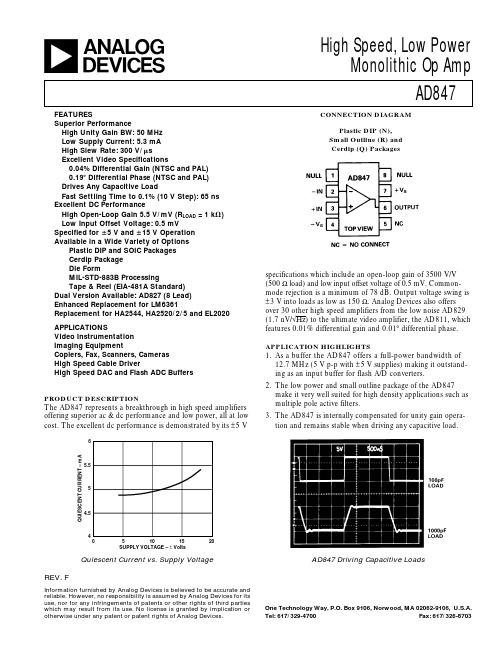
a
FEATURES Superior Performance
High Unity Gain BW: 50 MHz Low Supply Current: 5.3 mA High Slew Rate: 300 V/s Excellent Video Specifications
AD847 Driving Capacitive Loads
One Technology Way, P.O. Box 9106, Norwood, MA 02062-9106, U.S.A.
Tel: 617/329-4700
Fax: 617/326-8703
元器件交易网
QUIESCENT CURRENT – mA
5.5
5
4.5
4
0
5
10
15
20
SUPPLY VOLTAGE – ± Volts
Quiescent Current vs. Supply Voltage
REV. F
Information furnished by Analog Devices is believed to be accurate and reliable. However, no responsibility is assumed by Analog Devices for its use, nor for any infringements of patents or other rights of third parties which may result from its use. No license is granted by implication or otherwise under any patent or patent rights of Analog Devices.
半导体传感器AD623ARMZ中文规格书

0
0
1
2
3
4
5
WARM-UP TIME – Minutes
TPC 6. Change in Input Offset Voltage vs. Warm-Up Time
REV. D
–5–
AD626
CURRENT SENSOR INTERFACE A typical current sensing application, making use of the large common-mode range of the AD626, is shown in Figure 9. The current being measured is sensed across resistor RS. The value of RS should be less than 1 k⍀ and should be selected so that the average differential voltage across this resistor is typically 100 mV.
INPUT COMMON-MODE RANGE – V
Typical Performance Characteristics–AD626
25
20
15
؎VCM FOR SINGLE
AND DUAL SUPPLIES
10
5
؎VCM FOR DUAL
SUPPLIES ONLY
0
1
2
3
4
5
SUPPLY VOLTAGE – ؎V
To produce a full-scale output of +4 V, a gain of 40 is used adjustable by ±20% to absorb the tolerance in the sense resistor. Note that there is sufficient headroom to allow at least a 10% overrange (to +4.4 V).
AD8253ARMZ中文资料

Mil
Low
Grade Power
High Speed PGA
AD82201 AD82311 AD620 AD6271 AD8250
AD8221 AD85531 AD621 AD6231 AD8251
AD8222 AD85551 AD524 AD82231 AD8253
AD82241 AD85561 AD526Norwood, MA 02062-9106, U.S.A.
Tel: 781.329.4700
Fax: 781.461.3113
©2008 Analog Devices, Inc. All rights reserved.
It has a high bandwidth of 10 MHz, low THD of −110 dB, and fast settling time of 780 ns (maximum) to 0.001%. Offset drift and gain drift are guaranteed to 1.2 μV/°C and 10 ppm/°C, respectively, for G = 1000. In addition to its wide input common voltage range, it boasts a high common-mode rejection of 100 dB at G = 1000 from dc to 20 kHz. The combination of precision dc performance coupled with high speed capabilities makes the AD8253 an excellent candidate for data acquisition. Furthermore, this monolithic solution simplifies design and manufacturing and boosts performance of instrumentation by maintaining a tight match of internal resistors and amplifiers.
AD825-K考勤机硬件说明

AD825-K考勤机硬件说明1、镜片2、液晶显示器3、键盘区4、无效卡指示灯(红灯)5、有效卡指示灯(绿灯)6、电源指示灯7、蜂鸣器8、感应区外接电铃、电锁等RS232或RS485 DC9V 电源开关技术指标:1.外形尺寸:17.5cm×13cm×2.8cm2.读卡距离:5cm<ID卡<15cm、IC卡<5cm3.打卡速度:<0.2秒4.通信接口:RS232或RS4855.外接电源:DC 9v/600MA.6.存储容量:打卡16382多条记录,发卡8000多条7.工作环境:温度-10℃~50℃8.后备电池:5小时≤待机时间≤8小时9.传送速率:19200BPS按键说明:“UP ”上翻键“DOWN”下翻键“MENU”菜单键“ENTER”确认键“CLEAR”退出键“UP”+数字键“0”查看打卡记录“UP”+数字键“1”查看发卡记录“UP”+数字键“8”锁键盘MENU+数字键“0000”(初始密码)进入菜单设置状态按数字键“1”键设置系统密码输入四位数的系统密码+“ENTER”注:切记不要遗失密码按数字键“2”键设置考勤机地址输入两位数的地址号( 限1-99 )+“ENTER”注:同一系统中地址号不能重复按数字键“3”键设置日期时间(按UP或DOWN移动光标)输入设定日期时间+“ENTER”按数字键“4”键设置刷卡延时刷卡延时是指同一张卡在设定时间内不能重复打卡,设为00时00分没有限制按数字键“5”键设置字体(按UP或DOWN移动光标)选定字体+“ENTER”字体设置是用来考勤机硬件界面的简繁体字转换按数字键“6”键设置批量发卡键盘发卡N:表示逻辑卡号(可更改、即:工号)P:表示物理卡号(不可更改、即:唯一)发卡操作过程:当进入发卡状态后,出现逻辑卡号,可用默认卡号,也可手工改动,设好后再按Enter键,此时卡在机器上感应一下,然后会提示发卡成功,等待发第二张卡,依次下去……(此发卡需在人事资料中输入同样卡号,然后在软件中做发卡对应)。
AD8572AR-REEL7资料
Zero-Drift, Single-Supply, Rail-to-RailInput/Output Operational AmplifiersAD8571/AD8572/AD8574 Rev. BInformation furnished by Analog Devices is believed to be accurate and reliable. However, noresponsibility is assumed by Analog Devices for its use, nor for any infringements of patents or other rights of third parties that may result from its use. Specifications subject to change without notice. No license is granted by implication or otherwise under any patent or patent rights of Analog Devices. T rademarks and registered trademarks are the property of their respective owners. O ne Technology Way, P.O. Box 9106, Norwood, MA 02062-9106, U.S.A. Tel: 781.329.4700 Fax: 781.461.3113 ©2006 Analog Devices, Inc. All rights reserved.FEATURESLow offset voltage: 1 μVInput offset drift: 0.005 μV/°CRail-to-rail input and output swing5 V/2.7 V single-supply operationHigh gain, CMRR, PSRR: 130 dBUltralow input bias current: 20 pALow supply current: 750 μA/op ampOverload recovery time: 50 μsNo external capacitors requiredAPPLICATIONSTemperature sensorsPressure sensorsPrecision current sensingStrain gage amplifiersMedical instrumentationThermocouple amplifiersGENERAL DESCRIPTIONThis family of amplifiers has ultralow offset, drift, and bias current. The AD8571, AD8572, and AD8574 are single, dual, and quad amplifiers, respectively, featuring rail-to-rail input and output swings. All are guaranteed to operate from 2.7 V to 5 V single supply.The AD857x family provides benefits previously found only in expensive auto-zeroing or chopper-stabilized amplifiers. Using Analog Devices, Inc. topology, these zero-drift amplifiers combine low cost with high accuracy. (No external capacitors are required.) Using a patented spread-spectrum auto-zero technique, the AD857x family eliminates the intermodulation effects from interaction of the chopping function with the signal frequency in ac applications.With an offset voltage of only 1 μV and drift of 0.005 μV/°C, the AD857x family is perfectly suited for applications where error sources cannot be tolerated. Position and pressure sensors, medical equipment, and strain gage amplifiers benefit greatly from nearly zero drift over their operating temperature range. Many more systems require the rail-to-rail input and output swings provided by the AD857x family.V+OUT ANCNC–IN A+IN AV–NC114-1NC = NO CONNECTNC–IN A+IN AV–114-4Figure 1. 8-Lead MSOP(RM Suffix)Figure 2. 8-Lead SOIC(R Suffix)–IN A+IN AV–OUT B–IN B+IN BOUT A V+114-2–IN A+IN AV–OUT B–IN B+IN BOUT A V+114-5 (RU Suffix)Figure 4. 8-Lead SOIC(R Suffix)OUT A–IN A+IN AV++IN B–IN BOUT B114-3OUT A–IN A+IN AV++IN B–IN BOUT B114-6Figure 5. 14-Lead TSSOP(RU Suffix)Figure 6. 14-Lead SOIC(R Suffix)The AD857x family is specified for the extended industrial/ automotive (−40°C to +125°C) temperature range. The AD8571 single amplifier is available in 8-lead MSOP and narrow 8-lead SOIC packages. The AD8572 dual amplifier is available in8-lead narrow SOIC and 8-lead TSSOP surface mount packages. The AD8574 quad amplifier is available in narrow 14-lead SOIC and 14-lead TSSOP packages.AD8571/AD8572/AD8574Rev. B | Page 2 of 24TABLE OF CONTENTSFeatures..............................................................................................1 Applications.......................................................................................1 General Description.........................................................................1 Pin Configurations...........................................................................1 Revision History...............................................................................2 Specifications.....................................................................................3 5 V Electrical Characteristics......................................................3 2.7 V Electrical Characteristics...................................................4 Absolute Maximum Ratings............................................................5 Thermal Characteristics..............................................................5 ESD Caution..................................................................................5 Typical Performance Characteristics.............................................6 Functional Description..................................................................14 Amplifier Architecture..............................................................14 Basic Auto-Zero Amplifier Theory..........................................14 Auto-Zero Phase.........................................................................14 Amplification Phase...................................................................15 High Gain, CMRR, PSRR..........................................................16 Maximizing Performance T hrough Proper Layout................16 1/f Noise Characteristics...........................................................17 Random Auto-Zero Correction Eliminates Intermodulation Distortion....................................................................................17 Broadband and External Resistor Noise Considerations..........18 Output Overdrive Recovery......................................................18 Input Overvoltage Protection...................................................18 Output Phase Reversal...............................................................18 Capacitive Load Drive...............................................................19 Power-Up Behavior....................................................................19 Applications.....................................................................................20 5 V Precision Strain Gage Circuit............................................20 3 V Instrumentation Amplifier................................................20 High Accuracy Thermocouple Amplifier...............................20 Precision Current Meter............................................................21 Precision Voltage Comparator..................................................21 Outline Dimensions.......................................................................22 Ordering Guide.. (23)REVISION HISTORY09/06—Rev. A to Rev. BUpdated Format..................................................................Universal Renumbered Figures..........................................................Universal Changes to Figure 50......................................................................14 Changes to Figure 51......................................................................15 Changes to Figure 66......................................................................21 Updated Outline Dimensions.......................................................22 Changes to Ordering Guide..........................................................23 07/03—Rev. 0 to Rev. ARenumbered Figures..........................................................Universal Changes to Ordering Guide.............................................................4 Change to Figure 15.......................................................................16 Updated Outline Dimensions. (19)10/99—Revision 0: Initial VersionAD8571/AD8572/AD8574Rev. B | Page 3 of 24SPECIFICATIONS5 V ELECTRICAL CHARACTERISTICSV S = 5 V , V CM = 2.5 V , V O = 2.5 V , T A = 25°C, unless otherwise noted. Table 1.Parameter Symbol Conditions Min Typ Max Unit INPUT CHARACTERISTICS Offset Voltage V OS 1 5 μV −40°C ≤ T A ≤ +125°C 10 μV Input Bias Current I B 10 50 pA −40°C ≤ T A ≤ +125°C 1.0 1.5 nA Input Offset Current I OS 20 70 pA −40°C ≤ T A ≤ +125°C 150 200 pA Input Voltage Range 0 5 V Common-Mode Rejection Ratio CMRR V CM = 0 V to 5 V 120 140 dB −40°C ≤ T A ≤ +125°C 115 130 dBLarge Signal Voltage Gain 1A VO R L = 10 kΩ, V O = 0.3 V to 4.7 V 125 145 dB −40°C ≤ T A ≤ +125°C 120 135 dB Offset Voltage Drift ∆V OS /∆T −40°C ≤ T A ≤ +125°C 0.005 0.04 μV/°C OUTPUT CHARACTERISTICS Output Voltage High V OH R L = 100 kΩ to GND 4.99 4.998 V −40°C to +125°C 4.99 4.997 V R L = 10 kΩ to GND 4.95 4.98 V −40°C to +125°C 4.95 4.975 V Output Voltage Low V OL R L = 100 kΩ to V+ 1 10 mV −40°C to +125°C 2 10 mV R L = 10 kΩ to V+ 10 30 mV −40°C to +125°C 15 30 mV Short-Circuit Limit I SC ±25 ±50 mA −40°C to +125°C ±40 mA Output Current I O ±30 mA −40°C to +125°C ±15 mA POWER SUPPLY Power Supply Rejection Ratio PSRR V S = 2.7 V to 5.5 V 120 130 dB −40°C ≤ T A ≤ +125°C 115 130 dB Supply Current/Amplifier I SY V O = 0 V 850 975 μA −40°C ≤ T A ≤ +125°C 1000 1075 μA DYNAMIC PERFORMANCE Slew Rate SR R L = 10 kΩ 0.4 V/μs Overload Recovery Time 0.05 0.3 ms Gain Bandwidth Product GBP 1.5 MHz NOISE PERFORMANCE Voltage Noise e n p-p 0 Hz to 10 Hz 1.3 μV p-p e n p-p 0 Hz to 1 Hz 0.41 μV p-p Voltage Noise Density e n f = 1 kHz 51 nV/√Hz Current Noise Density i n f = 10 Hz 2 fA/√Hz1Gain testing is dependent upon test bandwidth.AD8571/AD8572/AD8574Rev. B | Page 4 of 242.7 V ELECTRICAL CHARACTERISTICS V S = 2.7 V , V CM = 1.35 V , V O = 1.35 V , T A = 25°C, unless otherwise noted.Table 2.Parameter Symbol Conditions Min Typ Max Unit INPUT CHARACTERISTICS Offset Voltage V OS 1 5 μV −40°C ≤ T A ≤ +125°C 10 μV Input Bias Current I B 10 50 pA −40°C ≤ T A ≤ +125°C 1.0 1.5 nA Input Offset Current I OS 10 50 pA −40°C ≤ T A ≤ +125°C 150 200 pA Input Voltage Range 0 2.7 V Common-Mode Rejection Ratio CMRR V CM = 0 V to 2.7 V 115 130 dB −40°C ≤ T A ≤ +125°C 110 130 dB Large Signal Voltage Gain 1A VO R L = 10 kΩ, V O = 0.3 V to 2.4 V 110 140 dB −40°C ≤ T A ≤ +125°C 105 130 dB Offset Voltage Drift ∆V OS /∆T −40°C ≤ T A ≤ +125°C 0.005 0.04 μV/°C OUTPUT CHARACTERISTICS Output Voltage High V OH R L = 100 kΩ to GND 2.685 2.697 V −40°C to +125°C 2.685 2.696 V R L = 10 kΩ to GND 2.67 2.68 V −40°C to +125°C 2.67 2.675 V Output Voltage Low V OL R L = 100 kΩ to V+ 1 10 mV −40°C to +125°C 2 10 mV R L = 10 kΩ to V+ 10 20 mV −40°C to +125°C 15 20 mV Short-Circuit Limit I SC ±10 ±15 mA −40°C to +125°C ±10 mA Output Current I O ±10 mA −40°C to +125°C ±5 mA POWER SUPPLY Power Supply Rejection Ratio PSRR V S = 2.7 V to 5.5 V 120 130 dB −40°C ≤ T A ≤ +125°C 115 130 dB Supply Current/Amplifier I SY V O = 0 V 750 900 μA −40°C ≤ T A ≤ +125°C 950 1000 μA DYNA MIC PERFOR MANCE Slew Rate SR R L = 10 kΩ 0.5 V/μs Overload Recovery Time 0.05 ms Gain Bandwidth Product GBP 1 MHz NOISE PERFOR MANCE Voltage Noise e n p-p 0 Hz to 10 Hz 2.0 μV p-p Voltage Noise Density e n f = 1 kHz 94 nV/√Hz Current Noise Density i n f = 10 Hz 2 fA/√Hz1Gain testing is dependent upon test bandwidth.AD8571/AD8572/AD8574Rev. B | Page 5 of 24ABSOLUTE MAXIMUM RATINGSTable 3.Parameter RatingSupply Voltage 6 VInput Voltage GND to V S + 0.3 VDifferential Input Voltage 1 ±5.0 VESD (Human Body Model) 2000 VOutput Short-Circuit Duration to GND IndefiniteStorage Temperature RangeRM, RU, and R Packages −65°C to +150°COperating Temperature RangeAD8571A/AD8572A/AD8574A −40°C to +125°CJunction Temperature RangeRM, RU, and R Packages −65°C to +150°C Lead Temperature Range (Soldering, 60 sec) 300°C1Differential input voltage is limited to ±5.0 V or the supply voltage, whichever is less.Stresses above those listed under Absolute Maximum Ratings may cause permanent damage to the device. This is a stress rating only; functional operation of the device at these or any other conditions above those indicated in the operationalsection of this specification is not implied. Exposure to absolute maximum rating conditions for extended periods may affect device reliability.THERMAL CHARACTERISTICSθJA is specified for the worst-case conditions, that is, θJA is specified for a device soldered in a circuit board for SOIC and TSSOP packages. Table 4. Thermal Resistance Package Type θJA θJC Unit 8-Lead MSOP (RM) 190 44 °C/W 8-Lead TSSOP (RU) 240 43 °C/W 8-Lead SOIC (R) 158 43 °C/W 14-Lead TSSOP (RU) 180 36 °C/W 14-Lead SOIC (R) 120 36 °C/W ESD CAUTIONAD8571/AD8572/AD8574Rev. B | Page 6 of 24TYPICAL PERFORMANCE CHARACTERISTICS180012010060204080140160–1.5–2.5–0.50.5 1.5 2.5N U M B E R O F A M P L I F I E R SOFFSET VOLTAGE (µV)01104-007Figure 7. Input Offset Voltage Distribution at 2.7 V50403020100–20–10–30I N P U T B I A S C U R R E N T (p A )INPUT COMMON-MODE VOLTAGE (V)01104-008Figure 8. Input Bias Current vs. Common-Mode Voltage1500–200010005000–1000–1500–500012345I N P U T B I A S C U R R E N T (p A )COMMON-MODE VOLTAGE (V)V S = 5V T A = 125°C01104-009Figure 9. Input Bias Current vs. Common-Mode Voltage 180012010060204080140160N U M B E R O F A M P L I F I E R SOFFSET VOLTAGE (µV)01104-010Figure 10. Input Offset Voltage Distribution at 5 V121086420123465N U M B E R O F A M P L I F I E R SINPUT OFFSET DRIFT (nV/°C)01104-011Figure 11. Input Offset Voltage Drift Distribution at 5 V10k1k1001010.1O U T P U T V O L T A G E (m V )LOAD CURRENT (mA)01104-012Figure 12. Output Voltage to Supply Rail vs. Output Current at 5 VAD8571/AD8572/AD8574Rev. B | Page 7 of 2410k1k 1001010.1O U T P U T V O L T A G E (m V )LOAD CURRENT (mA)01104-013Figure 13. Output Voltage to Supply Rail vs. Output Current at 2.7 V 1000750500250I N P U T B I A S C UR R E N T (p A )TEMPERATURE (°C)01104-014Figure 14. Bias Current vs. Temperature1.00.80.60.40.2S U P P L Y C U R R E N T (m A )TEMPERATURE (°C)01104-015Figure 15. Supply Current vs. Temperature 8002001003004005006007000S U P P L Y C U R R E N T P E R A M P L I F I E R (µA )SUPPLY VOLTAGE (V)01104-016Figure 16. Supply Current vs. Supply Voltage45901351802252700604050102030–100–40–30–20O P E N -L O O P G A I N (d B )P H A S E S H I F T (D e g r e e s )FREQUENCY (Hz)01104-017Figure 17. Open-Loop Gain and Phase Shift vs. Frequency at 2.7 V45901351802252700604050102030–100–40–30–2010k100k 1M10M 100MO P E N -LO O P G A I N (d B )P H A S E S H I F T (D e g r e e s )FREQUENCY (Hz)01104-018Figure 18. Open-Loop Gain and Phase Shift vs. Frequency at 5 VAD8571/AD8572/AD8574Rev. B | Page 8 of 24604050102030–100–40–30–2010010k1k1M100k10MC L O S ED -L O O P G A I N (d B )FREQUENCY (Hz)01104-019Figure 19. Closed-Loop Gain vs. Frequency at 2.7 V 604050102030–100–40–30–20C L O S ED -L O O P G A I N (d B )FREQUENCY (Hz)01104-020Figure 20. Closed-Loop Gain vs. Frequency at 5 V3002402701501802109012003060O U T P U T I M P E D A N C E (Ω)FREQUENCY (Hz)01104-021Figure 21. Output Impedance vs. Frequency at 2.7 V3002402701501802109012003060O U T P U T I M P E D A N C E (Ω)FREQUENCY (Hz)01104-022Figure 22. Output Impedance vs. Frequency at 5 V01104-023Figure 23. Large Signal Transient Response at 2.7 V01104-024Figure 24. Large Signal Transient Response at 5 VAD8571/AD8572/AD8574Rev. B | Page 9 of 2401104-025Figure 25. Small Signal Transient Response at 2.7 V 01104-026Figure 26. Small Signal Transient Response at 5 V101001k10kCAPACITANCE (pF)01104-027S M A L L S I G N A L O V E R S H O O T(%)50450403530252015105Figure 27. Small Signal Overshoot vs. Load Capacitance at 2.7 V450510152025303540S M A L L S I G N A L O V E R S H O O T (%)CAPACITANCE (pF)01104-028Figure 28. Small Signal Overshoot vs. Load Capacitance at 5 V0V V INV OUT0VBOTTOM SCALE: 1V/DIV TOP SCALE: 200mV/DIV01104-029Figure 29. Positive Overvoltage Recovery0VV IN V OUT0VBOTTOM SCALE: 1V/DIV TOP SCALE: 200mV/DIV01104-030Figure 30. Negative Overvoltage RecoveryAD8571/AD8572/AD8574Rev. B | Page 10 of 2401104-031Figure 31. No Phase ReversalC M R R (d B )FREQUENCY (Hz)14080100120600204001104-032Figure 32. CMRR vs. Frequency at 2.7 VC M R R (d B )FREQUENCY (Hz)1408010012060204001104-033Figure 33. CMRR vs. Frequency at 5 VP S R R (d B )FREQUENCY (Hz)14010012001104-034Figure 34. PSRR vs. Frequency at ±1.35 V10010k 1k 10MP S R R (d B )FREQUENCY (Hz)1408010012060204001104-0351M 100kFigure 35. PSRR vs. Frequency at ±2.5 VO U T P U T S W I N G (V p -p )FREQUENCY (Hz)3.01.52.02.51.000.501104-036Figure 36. Maximum Output Swing vs. Frequency at 2.7 VAD8571/AD8572/AD8574Rev. B | Page 11 of 24O U T P U T S W I N G (V p -p )FREQUENCY (Hz)01104-037Figure 37. Maximum Output Swing vs. Frequency at 5 V 0V01104-038Figure 38. 0.1 Hz to 10 Hz Noise at 2.7 V01104-039Figure 39. 0.1 Hz to 10 Hz Noise at 5 V31236420826010415652e n (n V H z )FREQUENCY (kHz)01104-040Figure 40. Voltage Noise Density at 2.7 V from 0 Hz to 2.5 kHz961126480324816e n (n V H z )FREQUENCY (kHz)1104-041Figure 41. Voltage Noise Density at 2.7 V from 0 Hz to 25 kHz156182104130527826e n (n V H z )FREQUENCY (kHz)01104-042Figure 42. Voltage Noise Density at 5 V from 0 Hz to 2.5 kHzAD8571/AD8572/AD8574Rev. B | Page 12 of 24961126480324816e n (n V H z )FREQUENCY (kHz)01104-043Figure 43. Voltage Noise Density at 5 V from 0 Hz to 25 kHz 180210120150609030e n (n V H z )FREQUENCY (kHz)01104-044Figure 44. Voltage Noise Density at 5 V from 0 Hz to 10 Hz150145140130135125P O W E R S U P P L Y R E J E C T I O N (d B )TEMPERATURE (°C)01104-045Figure 45. Power Supply Rejection vs. Temperature50304010–30–10200–40–20–50–75–50–250255075100125150S H OR T -C I R C U I T C U R R E N T (m A )TEMPERATURE (°C)01104-046Figure 46. Output Short-Circuit Current vs. TemperatureAD8571/AD8572/AD8574Rev. B | Page 13 of 24100608020–60–20400–80–40–100–75–50–25255075100125150S H O R T -C I R C U I T C U R R E N T (m A )TEMPERATURE (°C)01104-047Figure 47. Output Short-Circuit Current vs. TemperatureO U T P U T V O L T A G E S W I N G (m V )TEMPERATURE (°C)100250200015025507512517522501104-048Figure 48. Output Voltage to Supply Rail vs. TemperatureO U T P U T V O L T A G E S W I N G (m V )TEMPERATURE (°C)100250200015025507512517522501104-049Figure 49. Output Voltage to Supply Rail vs. TemperatureAD8571/AD8572/AD8574Rev. B | Page 14 of 24FUNCTIONAL DESCRIPTIONThe AD8571/AD8572/AD8574 are CMOS amplifiers that achieve their high degree of precision through randomfrequency auto-zero stabilization. The autocorrection topology allows the AD857x to maintain its low offset voltage over a wide temperature range, and the randomized auto-zero clockeliminates any intermodulation distortion (IMD) errors at the amplifier output.The AD857x can be run from a single-supply voltage as low as 2.7 V . The extremely low offset voltage of 1 μV and no IMD products allows the amplifier to be easily configured for high gains without risk of excessive output voltage errors. This makes the AD857x an ideal amplifier for applications requiring both dc precision and low distortion for ac signals. The extremely small temperature drift of 5 nV/°C ensures a minimum of offset voltage error over its entire temperature range of −40°C to +125°C. These combined features make the AD857x an excellent choice for a variety of sensitive measurement and automotive applications.AMPLIFIER ARCHITECTUREEach AD857x op amp consists of two amplifiers: a main amplifier and a secondary amplifier that is used to correct the offset voltage of the main amplifier. Both consist of a rail-to-rail input stage, allowing the input common-mode voltage range to reach both supply rails. The input stage consists of an NMOS differential pair operating concurrently with a parallel PMOS differential pair. The outputs from the differential input stages are combined in another gain stage whose output is used to drive a rail-to-rail output stage.The wide voltage swing of the amplifier is achieved by using two output transistors in a common-source configuration. The output voltage range is limited by the drain-to-source resistance of these transistors. As the amplifier is required to source or sink more output current, the voltage drop across these transistors increases due to their on resistance (rds). Simply put, the output voltage does not swing as close to the rail under heavy output current conditions as it does with light output current. This is a characteristic of all rail-to-rail output amplifiers. Figure 12 and Figure 13 show how close the output voltage can get to the rails with a given output current. The output of the AD857x is short-circuit protected to approximately 50 mA of current.The AD857x amplifiers have exceptional gain, yielding greater than 120 dB of open-loop gain with a load of 2 kΩ. Because the output transistors are configured in a common-source configura-tion, the gain of the output stage, and thus the open-loop gain of the amplifier, is dependent on the load resistance. Open-loop gain decreases with smaller load resistances. This is another characteristic of rail-to-rail output amplifiers.BASIC AUTO-ZERO AMPLIFIER THEORYAutocorrection amplifiers are not a new technology. Various IC implementations have been available for more than 15 years and some improvements have been made over time. The AD857x design offers a number of significant performance improve-ments over older versions while attaining a very substantial reduction in device cost. This section offers a simplified explanation of how the AD857x is able to offer extremely low offset voltages and high open-loop gains.As noted in the Amplifier Architecture section, each AD857x op amp contains two internal amplifiers. One is used as the primary amplifier, the other as an autocorrection, or nulling, amplifier. Each amplifier has an associated input offset voltage that can be modeled as a dc voltage source in series with the noninverting input. In Figure 50 and Figure 51, these are labeled as V OSX , where X denotes the amplifier associated with the offset: A for the nulling amplifier, B for the primary amplifier. The open-loop gain for the +IN and −IN inputs of each amplifier is given as A X . Both amplifiers also have a third voltage input with an associated open-loop gain of B X . There are two modes of operation determined by the action of two sets of switches in the amplifier: an auto-zero phase and an amplification phase.AUTO-ZERO PHASEIn this phase, all φA switches are closed and all φB switches are opened. Here, the nulling amplifier is taken out of the gain loop by shorting its two inputs together. Of course, there is a degree of offset voltage, shown as V OSA , inherent in the nulling amplifier that maintains a potential difference between the +IN and −IN inputs. The nulling amplifier feedback loop is closed through φA 2 and V OSA appears at the output of the nulling amp and on C M1, an internal capacitor in the AD857x. Mathematically, we can express this in the time domain as][][][t V B t V A t V OA A OSA A OA −= (1)this also can be expressed as[][]AOSA A OA B t V A t V +=1 (2)This shows that the offset voltage of the nulling amplifier times a gain factor appears at the output of the nulling amplifier and thus on the C M1 capacitor.AD8571/AD8572/AD8574Rev. B | Page 15 of 24V IN+V IN–V 01104-050Figure 50. Auto-Zero Phase of the AmplifierAMPLIFICATION PHASEWhen the φB switches close and the φA switches open for the amplification phase, this offset voltage remains on C M1 and essentially corrects any error from the nulling amplifier. The voltage across C M1 is designated as V NA . The potential difference between the two inputs to the primary amplifier is designated as V IN , or V IN = (V IN+ − V IN–). The output of the nulling amplifier can then be expressed as[][][][]t V B t V t V A t V NA A OSA IN A OA −−=( (3)V IN+VIN–V 01104-051Figure 51. Output Phase of the AmplifierBecause φA is now open and there is no place for C M1 to discharge, the voltage (V NA ) at the present time (t) is equal to the voltage at the output of the nulling amp (V OA ) at the time when φA was closed. If the period of the autocorrection switching frequency is designated as T S , then the amplifier switches between phases every 0.5 × T S . Therefore, in the amplification phase[]⎥⎦⎤⎢⎣⎡−=S NA NA T t V t V 21 (4) and substituting Equation 4 and Equation 2 into Equation 3yields[][][]AS OSA A A OSA A IN A OA B T t V B A t V A t V A t V +⎥⎦⎤⎢⎣⎡−−+=121(5) For the sake of simplification, it can be assumed that the autocorrection frequency is much faster than any potential change in V OSA or V OSB . This is a good assumption since changes in offset voltage are a function of temperature variation orlong-term wear time, both of which are much slower than the auto-zero clock frequency of the AD857x. This effectively makes the V OS time invariant, and Equation 5 can be rewritten as[][]()AOSAA A OSA A A IN A OAB V B A V B A t V A t V +−++=11 (6)or[][]⎟⎟⎠⎞⎜⎜⎝⎛++=A OSA IN A OA B V t V A t V 1 (7) Here, the auto-zeroing becomes apparent. Note that the V OSterm is reduced by a 1 + B A factor. This shows how the nulling amplifier has greatly reduced its own offset voltage error even before correcting the primary amplifier. Thus, the primary amplifier output voltage is the voltage at the output of the AD857x amplifier. It is equal to[][]()NB B OSB IN B OUT V B V t V A t V ++= (8)In the amplification phase, V OA = V NB , so this can be rewritten as[][][]⎥⎥⎦⎤⎢⎢⎣⎡⎟⎟⎠⎞⎜⎜⎝⎛++++=A OSA IN A B OSB B IN B OUT B V t V A B V A t V A t V 1 (9) combining terms yields[][]()OSBB AOSAB A B A B IN OUT V A B V B A B A A t V t V ++++=1 (10)The AD857x architecture is optimized in such a way thatA A = AB and B A = B B and B A >> 1. In addition, the gain product to A A B B is much greater than A B . Thus, Equation 10 can be simplified to[][])(OSB OSA A A A IN OUT V V A B A t V t V ++= (11)Most obvious is the gain product of both the primary and nulling amplifiers. This A A B A term is what gives the AD857x its extremely high open-loop gain. To understand how V OSA and V OSB relate to the overall effective input offset voltage of thecomplete amplifier, set up the generic amplifier equation of )(,EFFOS INOUTV V k V +×= (12)where k is the open-loop gain of an amplifier and V OS , EFF is its effective offset voltage. Putting Equation 12 into the form of Equation 11 gives[][]A A EFF OS A A IN OUT B A V B A t V t V ,+= (13) ThereforeAOSBOSA EFF OS B V V V +≈, (14)。
AD8321ARZ中文资料

Interactive CATV Set-Top Boxes
CATV Plant Test Equipment
General Purpose IF Variable Gain Block
VCC
Gain Programmable CATV Line Driver AD8321
FUNCTIONAL 43; INV VIN– ATTENUATOR CORE
PWR AMP VOUT REVERSE AMP
DATA LATCH DATA SHIFT REGISTER POWERDOWN/ SWITCH INTER PD
DATA SHIFT REGISTER
All Gain Codes f = 65 MHz f = 65 MHz All Gain Codes, Full Temperature Range Max Gain, f = 10 MHz Min Gain, f = 10 MHz Output Noise Temperature Sensitivity 0 £ TA £ +70∞C, Min Gain Power-Down Spectral Density 1 dB Compression Point Max Gain, f = 10 MHz Output Impedance Power-Up and Power-Down f = 42 MHz, POUT = 11 dBm, VCC = +9 V f = 65 MHz, POUT = 11 dBm, VCC = +9 V –40∞C £ TA £ +85∞C f = 10 MHz, All Gain Codes 0 £ TA £ +70∞C Min to Max Gain, VIN = 0 V Max Gain, VIN = 0.15 V Step Power Down, 65 MHz, Min Gain VIN = 0.137 V p-p Max Gain, VIN = 0 Max Gain, VIN = 0 Max Gain, VIN = 0 Max Gain, VIN = 0 Power-Up, VCC = +9 V Power-Down, VCC = +9 V
- 1、下载文档前请自行甄别文档内容的完整性,平台不提供额外的编辑、内容补充、找答案等附加服务。
- 2、"仅部分预览"的文档,不可在线预览部分如存在完整性等问题,可反馈申请退款(可完整预览的文档不适用该条件!)。
- 3、如文档侵犯您的权益,请联系客服反馈,我们会尽快为您处理(人工客服工作时间:9:00-18:30)。
Low Cost, General Purpose High Speed JFET Amplifier
AD825
CONNECTION DIAGRAM 8-Lead Plastic SOIC (R) Package
NC 1 –IN 2 +IN 3 –VS 4
AD825
TOP VIEW (Not to Scale)
INPUT OFFSET VOLTAGE
Offset Drift
Conditions
VS
Gain = +1 Gain = +1 RLOAD = 1 kΩ, G = 1 0 V–10 V Step, AV = –1 0 V–10 V Step, AV = –1 FC = 1 MHz, G = –1 NTSC Gain = +2 NTSC Gain = +2
8 NC 7 +VS 6 OUTPUT 5 NC
NC = NO CONNECT
Figure 1. Performance with Rail-to-Rail Input Signals
REV. C
Information furnished by Analog Devices is believed to be accurate and reliable. However, no responsibility is assumed by Analog Devices for its use, nor for any infringements of patents or other rights of third parties which may result from its use. No license is granted by implication or otherwise under any patent or patent rights of Analog Devices.
One Technology Way, P.O. Box 9106, Norwood, MA 02062-9106, U.S.A.
Tel: 781/329-4700 World Wide Web Site:
Fax: 781/326-8703
© Analog Devices, Inc., 1999
1
2
5
10
INPUT BIAS CURRENT INPUT OFFSET CURRENT OPEN LOOP GAIN
TMIN TMAX
TMIN TMAX
VOUT = ± 10 V RLOAD = 1 kΩ VOUT = ± 7.5 V RLOAD = 1 kΩ VOUT = ± 7.5 V RLOAD = 150 Ω (50 mA Output)
APPLICATIONS CCD Low Distortion Filters Mixed Gain Stages Audio Amplifier Photo Detector Interface ADC Input Buffer DAC Output Buffer
PRODUCT DESCRIPTION The AD825 is a superbly optimized operational amplifier for high speed, low cost and dc parameters, making it ideally suited for a broad range of signal conditioning and data acquisition applications. The ac performance, gain, bandwidth, slew rate and drive capability are all very stable over temperature. The AD825 also maintains stable gain under varying load conditions.
INPUT OFFSET VOLTAGE
Offset Drift
Gain = +1 Gain = +1 RLOAD = 1 kΩ, G = –1 –2.5 V to +2.5 V –2.5 V to +2.5 V FC = 1 MHz, G = –1 NTSC Gain = +2 NTSC Gain = +2
± 15 V
± 15 V
± 15 V ± 15 V ± 15 V
15 40 5
700
20 30 5
440
70
76
70
76
72
74Leabharlann COMMON-MODE REJECTION INPUT VOLTAGE NOISE INPUT CURRENT NOISE
VCM = ± 10 V f = 10 kHz f = 10 kHz
The AD825 is fully specified for operation with dual ± 5 V and ± 15 V supplies. This power supply flexibility, and the low supply current of 6.5 mA with excellent ac characteristics under all supply conditions, makes the AD825 well suited for many demanding applications.
± 15 V ± 15 V ± 15 V
71
80
12
10
INPUT COMMON-MODE VOLTAGE RANGE
± 15 V
± 13.5
OUTPUT VOLTAGE SWING
Output Current Short-Circuit Current INPUT RESISTANCE
RLOAD = 1 kΩ RLOAD = 500 Ω
The unique input stage has ultralow input bias current and ultralow input current noise. Signals that go to either rail on this high performance input do not cause phase reversals at the output. These features make the AD825 a good choice as a buffer for MUX outputs, creating minimal offset and gain errors.
Specifications subject to change without notice.
± 15 V ± 15 V
6.5 7.2 7.5
Units
MHz MHz MHz V/µs ns ns dB %
Degrees
mV mV µV/°C pA pA pA pA pA pA
dB
dB
dB
dB nV/√Hz fA/√Hz
TMIN to TMAX
INPUT BIAS CURRENT
INPUT OFFSET CURRENT Offset Current Drift
OPEN LOOP GAIN
COMMON-MODE REJECTION INPUT VOLTAGE NOISE
TMIN TMAX
TMIN TMAX VOUT = ± 2.5 V RLOAD = 500 Ω RLOAD = 150 Ω VCM = ± 2 V
TMIN to TMAX
± 15 V ± 15 V ± 15 V ± 15 V ± 15 V ± 15 V ± 15 V ± 15 V
± 15 V
± 15 V
␣ ␣ ␣ ␣ ␣ ␣ ␣ ␣ AD825A
Min
Typ Max
23
26
18
21
44
46
125
140
150 180
180 220
–77
1.3
2.1
f = 10 kHz
INPUT CURRENT NOISE
f = 10 kHz
INPUT COMMON-MODE VOLTAGE RANGE
OUTPUT VOLTAGE SWING
Output Current Short-Circuit Current
RLOAD = 500 Ω RLOAD = 150 Ω
元器件交易网
a
FEATURES High Speed
41 MHz, –3 dB Bandwidth 125 V/s Slew Rate 80 ns Settling Time Input Bias Current of 20 pA and Noise Current of 10 fA/√Hz Input Voltage Noise of 12 nV/√Hz Fully Specified Power Supplies: ؎5 V to ؎15 V Low Distortion: –76 dB at 1 MHz High Output Drive Capability Drives Unlimited Capacitance Load 50 mA Min Output Current No Phase Reversal When Input Is at Rail Available in 8-Lead SOIC
V V V mA mA Ω pF Ω
mA mA
–2–
REV. C
元器件交易网
SPECIFICATIONS (@ TA = +25؇C, VS = ؎5 V unless otherwise noted)