74F241SC中文资料
关于74HC244芯片的中文资料

电源电压Vcc 54 4.5 5 5.5 V
74 4.75 5 5.25
输入高电平电ViH 2 V
输入低电平电ViL 54 0.7 V
74 0.8
输出高电平电流IOH 54 -12 mA
74 -15
输出低电平电流IOL 54 12 mA
74 24
求关于74HC244线接收器(3S,两组控制)
简要说明:
244为三态输出的八组缓冲器和总线驱动器,其主要电器特性的典型值如下(不同厂家具体值有差别):
型号 tPLH tphl PD
54LS241/74LS241 12ns 12ns 110mW
引出端符号:
1A1~1A4,2A1~2A4 输入端
/1G, /2G 三态允许端(低电平有效)
1Y1~1Y4,2Y1~2Y4 输出端
逻辑图:
双列直插封装
极限值:
电源电压 …………………………………………. 7V
输入电压 …………………………………………. 5.5V
tPHZ输出由高到高阻态禁止时间 Vcc=5V CL=5pF
RL=90 Ω 18 ns
tPLZ输出由低到高阻态禁止时间 25 ns
静态特性(TA为工作环境温度范围)
参 数 测 试 条 件【1】 LS244 单位
最小 最大
VIK输入嵌位电压 Vcc=最小,Iik=-18mA -1.5 V
输出高阻态时高电平电压 …………………………. 5.5V
工作环境温度
54XXX …………………………………. -55~125℃
74XXX …………………………………. 0~70℃
SN74BCT241DW,SN74BCT241DWE4,SN74BCT241DWG4,SN74BCT241N,SN74BCT241NE4, 规格书,Datasheet 资料
Addendum-Page 1PACKAGING INFORMATIONOrderable Device Status(1)Package Type PackageDrawingPins Package QtyEco Plan(2)Lead/Ball Finish MSL Peak Temp (3)Samples (Requires Login)5962-9074301M2A ACTIVE LCCC FK 201TBD Call TI Call TI 5962-9074301MRA ACTIVE CDIP J 201TBD Call TI Call TI 5962-9074301MSA ACTIVE CFP W 201TBD Call TI Call TI SN74BCT241DBLE OBSOLETE SSOP DB 20TBDCall TICall TISN74BCT241DW ACTIVE SOIC DW 2025Green (RoHS & no Sb/Br)CU NIPDAU Level-1-260C-UNLIM SN74BCT241DWE4ACTIVE SOIC DW 2025Green (RoHS & no Sb/Br)CU NIPDAU Level-1-260C-UNLIM SN74BCT241DWG4ACTIVE SOIC DW 2025Green (RoHS & no Sb/Br)CU NIPDAU Level-1-260C-UNLIM SN74BCT241N ACTIVE PDIP N 2020Pb-Free (RoHS)CU NIPDAU N / A for Pkg Type SN74BCT241NE4ACTIVE PDIP N 2020Pb-Free (RoHS)CU NIPDAU N / A for Pkg Type SN74BCT241NSR ACTIVE SO NS 20Green (RoHS & no Sb/Br)CU NIPDAU Level-1-260C-UNLIM SN74BCT241NSRE4ACTIVE SO NS 20Green (RoHS & no Sb/Br)CU NIPDAU Level-1-260C-UNLIM SN74BCT241NSRG4ACTIVE SO NS 20Green (RoHS & no Sb/Br)CU NIPDAU Level-1-260C-UNLIM SNJ54BCT241FK ACTIVE LCCC FK 201TBD POST-PLATE N / A for Pkg TypeSNJ54BCT241J ACTIVE CDIP J 201TBD A42N / A for Pkg Type SNJ54BCT241WACTIVECFPW201TBDCall TIN / A for Pkg Type(1)The marketing status values are defined as follows:ACTIVE: Product device recommended for new designs.LIFEBUY: TI has announced that the device will be discontinued, and a lifetime-buy period is in effect.NRND: Not recommended for new designs. Device is in production to support existing customers, but TI does not recommend using this part in a new design.PREVIEW: Device has been announced but is not in production. Samples may or may not be available.OBSOLETE: TI has discontinued the production of the device.(2)Eco Plan - The planned eco-friendly classification: Pb-Free (RoHS), Pb-Free (RoHS Exempt), or Green (RoHS & no Sb/Br) - please check /productcontent for the latest availability information and additional product content details.TBD: The Pb-Free/Green conversion plan has not been defined.Pb-Free (RoHS): TI's terms "Lead-Free" or "Pb-Free" mean semiconductor products that are compatible with the current RoHS requirements for all 6 substances, including the requirement that lead not exceed 0.1% by weight in homogeneous materials. Where designed to be soldered at high temperatures, TI Pb-Free products are suitable for use in specified lead-free processes.芯天下--/Pb-Free (RoHS Exempt): This component has a RoHS exemption for either 1) lead-based flip-chip solder bumps used between the die and package, or 2) lead-based die adhesive used between the die and leadframe. The component is otherwise considered Pb-Free (RoHS compatible) as defined above.Green (RoHS & no Sb/Br): TI defines "Green" to mean Pb-Free (RoHS compatible), and free of Bromine (Br) and Antimony (Sb) based flame retardants (Br or Sb do not exceed 0.1% by weight in homogeneous material)(3) MSL, Peak Temp. -- The Moisture Sensitivity Level rating according to the JEDEC industry standard classifications, and peak solder temperature.Important Information and Disclaimer:The information provided on this page represents TI's knowledge and belief as of the date that it is provided. TI bases its knowledge and belief on information provided by third parties, and makes no representation or warranty as to the accuracy of such information. Efforts are underway to better integrate information from third parties. TI has taken and continues to take reasonable steps to provide representative and accurate information but may not have conducted destructive testing or chemical analysis on incoming materials and chemicals. TI and TI suppliers consider certain information to be proprietary, and thus CAS numbers and other limited information may not be available for release.In no event shall TI's liability arising out of such information exceed the total purchase price of the TI part(s) at issue in this document sold by TI to Customer on an annual basis.OTHER QUALIFIED VERSIONS OF SN54BCT241, SN74BCT241 :•Catalog: SN74BCT241•Military: SN54BCT241NOTE: Qualified Version Definitions:•Catalog - TI's standard catalog product•Military - QML certified for Military and Defense ApplicationsAddendum-Page 2芯天下--/TAPE AND REEL INFORMATION*All dimensions are nominalDevicePackage Type Package Drawing Pins SPQReel Diameter (mm)Reel Width W1(mm)A0(mm)B0(mm)K0(mm)P1(mm)W (mm)Pin1Quadrant SN74BCT241NSR SONS20330.024.48.213.02.512.024.0Q1*All dimensions are nominalDevice Package Type Package Drawing Pins SPQ Length(mm)Width(mm)Height(mm)SN74BCT241NSR SO NS200367.0367.045.0IMPORTANT NOTICETexas Instruments Incorporated and its subsidiaries(TI)reserve the right to make corrections,enhancements,improvements and other changes to its semiconductor products and services per JESD46C and to discontinue any product or service per JESD48B.Buyers should obtain the latest relevant information before placing orders and should verify that such information is current and complete.All semiconductor products(also referred to herein as“components”)are sold subject to TI’s terms and conditions of sale supplied at the time of order acknowledgment.TI warrants performance of its components to the specifications applicable at the time of sale,in accordance with the warranty in TI’s terms and conditions of sale of semiconductor products.Testing and other quality control techniques are used to the extent TI deems necessary to support this warranty.Except where mandated by applicable law,testing of all parameters of each component is not necessarily performed.TI assumes no liability for applications assistance or the design of Buyers’products.Buyers are responsible for their products and applications using TI components.To minimize the risks associated with Buyers’products and applications,Buyers should provide adequate design and operating safeguards.TI does not warrant or represent that any license,either express or implied,is granted under any patent right,copyright,mask work right,or other intellectual property right relating to any combination,machine,or process in which TI components or services are rmation published by TI regarding third-party products or services does not constitute a license to use such products or services or a warranty or endorsement e of such information may require a license from a third party under the patents or other intellectual property of the third party,or a license from TI under the patents or other intellectual property of TI.Reproduction of significant portions of TI information in TI data books or data sheets is permissible only if reproduction is without alteration and is accompanied by all associated warranties,conditions,limitations,and notices.TI is not responsible or liable for such altered rmation of third parties may be subject to additional restrictions.Resale of TI components or services with statements different from or beyond the parameters stated by TI for that component or service voids all express and any implied warranties for the associated TI component or service and is an unfair and deceptive business practice. TI is not responsible or liable for any such statements.Buyer acknowledges and agrees that it is solely responsible for compliance with all legal,regulatory and safety-related requirements concerning its products,and any use of TI components in its applications,notwithstanding any applications-related information or support that may be provided by TI.Buyer represents and agrees that it has all the necessary expertise to create and implement safeguards which anticipate dangerous consequences of failures,monitor failures and their consequences,lessen the likelihood of failures that might cause harm and take appropriate remedial actions.Buyer will fully indemnify TI and its representatives against any damages arising out of the use of any TI components in safety-critical applications.In some cases,TI components may be promoted specifically to facilitate safety-related applications.With such components,TI’s goal is to help enable customers to design and create their own end-product solutions that meet applicable functional safety standards and requirements.Nonetheless,such components are subject to these terms.No TI components are authorized for use in FDA Class III(or similar life-critical medical equipment)unless authorized officers of the parties have executed a special agreement specifically governing such use.Only those TI components which TI has specifically designated as military grade or“enhanced plastic”are designed and intended for use in military/aerospace applications or environments.Buyer acknowledges and agrees that any military or aerospace use of TI components which have not been so designated is solely at the Buyer's risk,and that Buyer is solely responsible for compliance with all legal and regulatory requirements in connection with such use.TI has specifically designated certain components which meet ISO/TS16949requirements,mainly for automotive ponents which have not been so designated are neither designed nor intended for automotive use;and TI will not be responsible for any failure of such components to meet such requirements.Products ApplicationsAudio /audio Automotive and Transportation /automotiveAmplifiers Communications and Telecom /communicationsData Converters Computers and Peripherals /computersDLP®Products Consumer Electronics /consumer-appsDSP Energy and Lighting /energyClocks and Timers /clocks Industrial /industrialInterface Medical /medicalLogic Security /securityPower Mgmt Space,Avionics and Defense /space-avionics-defense Microcontrollers Video and Imaging /videoRFID OMAP Mobile Processors /omap TI E2E Community Wireless Connectivity /wirelessconnectivityMailing Address:Texas Instruments,Post Office Box655303,Dallas,Texas75265Copyright©2012,Texas Instruments Incorporated。
M74HCT241资料

M54HCT240/241/244M74HCT240/241/244Septembe r 1993HCT240:INVERTED -HCT241/244NON INVERTEDOCTAL BUS BUFFER WITH 3STATE OUTPUTS B1R(Plastic Package)ORDER CODES :M54HCTXXXF1R M74HCTXXXM1R M74HCTXXXB1R M74HCTXXXC1RF1R(Ceramic Package)M1R(Micro Package)C1R (Chip Carrier)PIN CONNECTION (top view).HIGH SPEEDt PD =13ns (TYP.)at V CC =5V .LOW POWER DISSIPATIONI CC =4µA (MAX.)at T A =25oC.COMPATIBLE WITH TTL OUTPUTS V IH =2V (MIN.)V IL =0.8V (MAX).OUTPUT DRIVE CAPABILITY 15LSTTL LOADS.SYMMETRICAL OUTPUT IMPEDANCE |I OH |=I OL =6mA (MIN).BALANCED PROPAGATION DELAYS t PLH =t PHL.PIN AND FUNCTION COMPATIBLE WITH 54/74LS240/241/244DESCRIPTIONThe M54/74HCT240,HCT241and HCT244are high speed CMOS OCTAL BUS BUFFERs fabricated in silicon gate C 2MOS technology.They have the same high speed performance of LSTTL combined with true CMOS low power consumption.The designer has a choise of select combination of inverting and non-inverting outputs,symmetrical G (active low output control)input,and complementary G and G inputs.Each control input governs four BUS BUFFERs.This integrated circuit has input and output characteristics that are fully compatible with 54/74LSTTL logic families.M54/74HCT devices are designed to directly interface HSC 2MOS systems with TTL and NMOS components.They are also plug in replacements for LSTTL devices giving a reduction of power consumption.These devices are designed to be used with 3state memory address drivers,etc.All inputs are equipp ed with protection circuits against static discharge and transient excess voltage.HCT244HCT241HCT2401/12CHIP CARRIERINPUT AND OUTPUT EQUIVALENT CIRCUIT PIN DESCRIPTION (HCT240)PIN No SYMBOL NAME AND FUNCTION 11G Output Enable Input 2,4,6,81A1to 1A4Data Inputs 9,7,5,32Y1to 2Y4Data Outputs 11,13,15,172A1to 2A4Data Inputs 18,16,14,121Y1to 1Y4Data Outputs 192G Output Enabel Input 10GND Ground (0V)20V CCPositive Supply VoltagePIN DESCRIPTION (HCT244)PIN No SYMBOL NAME AND FUNCTION 11G Output Enable Input 2,4,6,81A1to 1A4Data Inputs 9,7,5,32Y1to 2Y4Data Outputs 11,13,15,172A1to 2A4Data Inputs 18,16,14,121Y1to 1Y4Data Outputs 192G Output Enabel Input 10GND Ground (0V)20V CCPositive Supply VoltagePIN DESCRIPTION (HCT241)PIN No SYMBOL NAME AND FUNCTION 11G Output Enable Input 2,4,6,81A1to 1A4Data Inputs 9,7,5,32Y1to 2Y4Data Outputs 11,13,15,172A1to 2A4Data Inputs 18,16,14,121Y1to 1Y4Data Outputs 192G Output Enabel Input 10GND Ground (0V)20V CCPositive Supply VoltageHCT244HCT241HCT240M54/M74HCT240/241/2442/12IEC LOGIC SYMBOLSTRUTH TABLEINPUTOUTPUTG G (HCT241)An Yn (HCT240)Yn (HCT241)Yn (HCT244)L H L H L L L HH LHHHLXZZZX:”H”or ”L”Z:High impeda nceCIRCUIT SCHEMATIC (1/8PACKAGE)HCT244HCT241HCT240HCT240HCT241/244M54/M74HCT240/241/2443/12ABSOLUTE MAXIMUM RATINGSSymbol Parameter Value Unit V CC Supply Voltage-0.5to+7V V I DC Input Voltage-0.5to V CC+0.5V V O DC Output Voltage-0.5to V CC+0.5VI IK DC Input Diode Current±20mAI OK DC Output Diode Current±20mAI O DC Output Source Sink Current Per Output Pin±35mAI CC or I GND DC V CC or Ground Current±70mAP D Power Dissipation500(*)mW T stg Storage Temperature-65to+150o C T L Lead Temperature(10sec)300o C Absolute Maximum Ratings are those values beyond whichdamage to the device may occu r.Functiona l ope ration und er these cond ition isnotimplied. (*)500mW:≅65o C derate to300mW by10mW/o C:65o C to85o CRECOMMENDED OPERATING CONDITIONSSymbol Parameter Value Unit V CC Supply Voltage 4.5to5.5V V I Input Voltage0to V CC V V O Output Voltage0to V CC VT op Operating Temperature:M54HC SeriesM74HC Series -55to+125-40to+85o Co Ct r,t f Input Rise and Fall Time(V CC=4.5to5.5V)0to500ns M54/M74HCT240/241/2444/12DC SPECIFICATIONSSymbol ParameterTest Conditions ValueUnit V CC(V)T A=25o C54HC and74HC-40to85o C74HC-55to125o C54HCMin.Typ.Max.Min.Max.Min.Max.V IH High Level InputVoltage 4.5to5.52.0 2.0 2.0VV IL Low Level InputVoltage 4.5to5.50.80.80.8VV OH High LevelOutput Voltage4.5V I=V IHorV ILI O=-20µA 4.4 4.5 4.4 4.4VI O=-6.0mA 4.18 4.31 4.13 4.10V OL Low Level OutputVoltage4.5V I=V IHorV ILI O=20µA0.00.10.10.1VI O=6.0mA0.170.260.330.4I I Input LeakageCurrent 5.5V I=V CC or GND±0.1±1±1µAI CC Quiescent SupplyCurrent5.5V I=V CC or GND44080µA∆I CC Additional worstcase supplycurrent 5.5Per Input pinV I=0.5V or2.4VOther Inputs atV CC or GND2.0 2.93.0mAM54/M74HCT240/241/2445/12AC ELECTRICAL CHARACTERISTICS(C L=50pF,Input t r=t f=6ns)Symbol ParameterTest Conditions ValueUnit V CC(V)C L(pF)T A=25o C54HC and74HC-40to85o C74HC-55to125o C54HCMin.Typ.Max.Min.Max.Min.Max.t TLH t THL Output TransitionTime4.5507121518nst PLH t PHL PropagationDelay Time4.55015222833ns4.515021303845nst PLH t PHL PropagationDelay Time4.55015253138ns4.515021334150nst PZL t PZH Output EnableTime4.550R L=1KΩ17303845ns4.5150R L=1KΩ23384857nst PLZ t PHZ Output DisableTime4.550R L=1KΩ16303845nsC IN Input Capacitance5101010pF C OUT OutputCapacitance10pFC PD(*)Power DissipationCapacitanceHCT240HCT241/2443331pF(*)C PD is defined as the value of the IC’s internal equivalent capac itanc e which is calculated from the operating current con sump tion without load. (Refer to Test Circuit).Average operting current can be obtained by the following equ ation.I CC(opr)=C PD•V CC•f IN+I CC/8(per circuit)TEST CIRCUIT I CC(Opr.)HCT240M54/M74HCT240/241/2446/12M54/M74HCT240/241/244 SWITCHING CHARACTERISTICS TEST WAVEFORM7/12M54/M74HCT240/241/244Plastic DIP20(0.25)MECHANICAL DATAmm inch DIM.MIN.TYP.MAX.MIN.TYP.MAX.a10.2540.010B 1.39 1.650.0550.065b0.450.018b10.250.010D25.4 1.000 E8.50.335e 2.540.100e322.860.900F7.10.280I 3.930.155L 3.30.130Z 1.340.053P001J 8/12M54/M74HCT240/241/244 Ceramic DIP20MECHANICAL DATAmm inchDIM.MIN.TYP.MAX.MIN.TYP.MAX.A250.984B7.80.307D 3.30.130E0.5 1.780.0200.070e322.860.900F 2.29 2.790.0900.110G0.40.550.0160.022I 1.27 1.520.0500.060L0.220.310.0090.012M0.51 1.270.0200.050N14°(min.),15°(max.)P7.98.130.3110.320Q 5.710.225P057H9/12M54/M74HCT240/241/244SO20MECHANICAL DATAmm inch DIM.MIN.TYP.MAX.MIN.TYP.MAX.A 2.650.104a10.100.200.0040.007 a2 2.450.096 b0.350.490.0130.019 b10.230.320.0090.012 C0.500.020c145°(typ.)D12.6013.000.4960.512 E10.0010.650.3930.419e 1.270.050e311.430.450F7.407.600.2910.299 L0.50 1.270.190.050 M0.750.029 S8°(max.)P013L 10/12M54/M74HCT240/241/244PLCC20MECHANICAL DATAmm inchDIM.MIN.TYP.MAX.MIN.TYP.MAX.A9.7810.030.3850.395B8.899.040.3500.356D 4.2 4.570.1650.180d1 2.540.100d20.560.022E7.378.380.2900.330e 1.270.050e3 5.080.200F0.380.015G0.1010.004M 1.270.050M1 1.140.045P027A11/12M54/M74HCT240/241/244Information furnished is believed to be accurate and reliable.However,SGS-THOMSON Microelectronics assumes no responsability for the consequences of use of such information nor for any infringement of patents or other rights of third parties which may results from its use.No license is granted by implication or otherwise under any patent or patent rights of SGS-THOMSON Microelectronics.Specificationsmentioned in this publication are subject to change without notice.This publication supersedes and replaces all information previously supplied.SGS-THOMSON Microelectronics products are not authorized for use ascritical components in life support devices or systems without express written approval of SGS-THOMSON Microelectonics.©1994SGS-THOMSON Microelectronics-All Rights ReservedSGS-THOMSON Microelectronics GROUP OF COMPANIESAustralia-Brazil-France-Germany-Hong Kong-Italy-Japan-Korea-Malaysia-Malta-Morocco-The Netherlands-Singapore-Spain-Sweden-Switzerland-Taiwan-Thailand-United Kingdom-U.S.A12/12。
74F241SJ中文资料
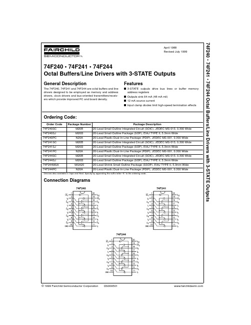
© 1999 Fairchild Semiconductor Corporation DS009501April 1988Revised July 199974F240 • 74F241 • 74F244 Octal Buffers/Line Drivers with 3-STATE Outputs74F240 • 74F241 • 74F244Octal Buffers/Line Drivers with 3-STATE OutputsGeneral DescriptionThe 74F240, 74F241 and 74F244 are octal buffers and line drivers designed to be employed as memory and address drivers, clock drivers and bus-oriented transmitters/receiv-ers which provide improved PC and board density.Featuress 3-STATE outputs drive bus lines or buffer memory address registers s Outputs sink 64 mA (48 mA mil)s 12 mA source currents Input clamp diodes limit high-speed termination effectsOrdering Code:Devices also available in T ape and Reel. Specify by appending the suffix letter “X” to the ordering code.Connection Diagrams74F24074F24174F244Order Code Package NumberPackage Description74F240SC M20B 20-Lead Small Outline Integrated Circuit (SOIC), JEDEC MS-013, 0.300 Wide 74F240SJ M20D 20-Lead Small Outline Package (SOP), EIAJ TYPE II, 5.3mm Wide 74F240PC N20A 20-Lead Plastic Dual-In-Line Package (PDIP), JEDEC MS-001, 0.300 Wide 74F241SC M20B 20-Lead Small Outline Integrated Circuit (SOIC), JEDEC MS-013, 0.300 Wide 74F241SJ M20D 20-Lead Small Outline Package (SOP), EIAJ TYPE II, 5.3mm Wide 74F241PC N20A 20-Lead Plastic Dual-In-Line Package (PDIP), JEDEC MS-001, 0.300 Wide 74F244SC M20B 20-Lead Small Outline Integrated Circuit (SOIC), JEDEC MS-013, 0.300 Wide 74F244SJ M20D 20-Lead Small Outline Package (SOP), EIAJ TYPE II, 5.3mm Wide 74F244MSA MSA2020-Lead Shrink Small Outline Package (SSOP), EIAJ TYPE II, 5.3mm Wide 74F244PCN20A20-Lead Plastic Dual-In-Line Package (PDIP), JEDEC MS-001, 0.300 Wide 274F 240 • 74F 241 • 74F 244Logic SymbolsIEEE/IEC 74F240IEEE/IEC 74F241IEEE/IEC 74F244Unit Loading/Fan OutNote 1: Worst-case 74F240 enabled; 74F241, 74F244 disabledTruth Tables74F24074F24174F244H = HIGH Voltage Level L = LOW Voltage Level X = ImmaterialZ = High ImpedancePin Names DescriptionU.L.Input I IH /I IL HIGH/LOW Output I OH /I OL OE 1, OE 23-STATE Output Enable Input (Active LOW) 1.0/1.66720 µA/−1 mA OE 23-STATE Output Enable Input (Active HIGH) 1.0/1.66720 µA/−1 mA I 0–I 7Inputs (74F240) 1.0/1.667 (Note 1)20 µA/−1 mA I 0–I 7Inputs (74F241, 74F244)1.0/2.667 (Note 1)20 µA/−1.6 mA O 0–O 7, O 0–O 7Outputs600/106.6 (80)−12 mA/64 mA (48 mA)OE 1D 1n O 1n OE 2D 2n O 2n H X Z H X Z L H L L H L LLH LLHOE 1D 1n O 1n OE 2D 2n O 2n H X Z L X Z L H H H H H LLLHLLOE 1D 1n O 1n OE 2D 2n O 2n H X Z H X Z L H H L H H LLLLLL74F240 • 74F241 • 74F244Absolute Maximum Ratings (Note 2)Recommended Operating ConditionsNote 2: Absolute maximum ratings are values beyond which the device may be damaged or have its useful life impaired. Functional operation under these conditions is not implied.Note 3: Either voltage limit or current limit is sufficient to protect inputs.DC Electrical CharacteristicsStorage Temperature−65°C to +150°C Ambient Temperature under Bias −55°C to +125°C Junction Temperature under Bias −55°C to +150°C V CC Pin Potential to Ground Pin −0.5V to +7.0V Input Voltage (Note 3)−0.5V to +7.0V Input Current (Note 3)−30 mA to +5.0 mAVoltage Applied to Output in HIGH State (with V CC = 0V)Standard Output −0.5V to V CC 3-STATE Output −0.5V to +5.5V Current Applied to Output in LOW State (Max)twice the rated I OL (mA)ESD Last Passing Voltage (Min)4000V Free Air Ambient Temperature 0°C to +70°C Supply Voltage+4.5V to +5.5VSymbol ParameterMin TypMaxUnits V CCConditionsV IH Input HIGH Voltage 2.0V Recognized as a HIGH Signal V IL Input LOW Voltage 0.8V Recognized as a LOW Signal V CD Input Clamp Diode Voltage −1.2VMin I IN = −18 mA V OHOutput HIGH 10% V CC 2.4VMinI OH = −3 mA Voltage10% V CC 2.0I OH = −15 mA 5% V CC 2.7I OH = −3 mA V OL Output LOW 10% V CC 0.55V Min I OL = 64 mA VoltageI IH Input HIGH 5.0µA Max V IN = 2.7V CurrentI BVI Input HIGH Current 7.0µA Max V IN = 7.0V Breakdown Test I CEX Output HIGH 50µA Max V OUT = V CC Leakage Current V ID Input Leakage 4.75V 0.0I ID = 1.9 µATestAll Other Pins Grounded I OD Output Leakage 3.75µA 0.0V IOD = 150 mVCircuit Current All Other Pins GroundedI IL Input LOW Current −1.0mAMaxV IN = 0.5V (OE 1, OE 2, OE 2, D n 74F240))−1.6V IN = 0.5V (D n (74F241, 74F244))I OZH Output Leakage Current 50µA Max V OUT = 2.7V I OZL Output Leakage Current −50µA Max V OUT = 0.5V I OS Output Short-Circuit Current −100−225mA Max V OUT = 0V I ZZ Bus Drainage Test500µA 0.0V V OUT = 5.25V I CCH Power Supply Current (74F240)1929mA Max V O = HIGH I CCL Power Supply Current (74F240)5075mA Max V O = LOW I CCZ Power Supply Current (74F240)4263mA Max V O = HIGH Z I CCH Power Supply Current 4060mA Max V O = HIGH (74F241, 74F244)I CCL Power Supply Current 6090mA Max V O = LOW (74F241, 74F244)I CCZPower Supply Current 6090mAMaxV O = HIGH Z(74F241, 74F244) 474F 240 • 74F 241 • 74F 244AC Electrical CharacteristicsSymbolParameterT A = +25°CT A = −55°C to +125°CT A = 0°C to +70°CUnitsV CC = +5.0V V CC = 5.0V V CC = 5.0V C L = 50 pFC L = 50 pF C L = 50 pF MinTyp Max Min Max Min Max t PLH Propagation Delay 3.0 5.17.0 3.09.0 3.08.0ns t PHL Data to Output (74F240) 2.0 3.5 4.7 2.0 6.0 2.0 5.7t PZH Output Enable Time (74F240)2.03.54.7 2.0 6.5 2.05.7ns t PZL 4.06.99.0 4.010.5 4.010.0t PHZ Output Disable Time (74F240) 2.0 4.0 5.3 2.0 6.5 2.0 6.3t PLZ 2.0 6.08.0 2.012.5 2.09.5t PLH Propagation Delay2.5 4.0 5.2 2.0 6.5 2.5 6.2ns t PHL Data to Output (74F241, 74F244) 2.5 4.0 5.2 2.07.0 2.5 6.5t PZH Output Enable Time 2.0 4.3 5.7 2.07.0 2.0 6.7ns t PZL (74F241, 74F244) 2.0 5.47.0 2.08.5 2.08.0t PHZ Output Disable Time 2.0 4.5 6.0 2.07.0 2.07.0t PLZ(74F241, 74F244)2.04.56.02.07.52.07.074F240 • 74F241 • 74F244Physical Dimensions inches (millimeters) unless otherwise noted20-Lead Small Outline Integrated Circuit (SOIC), JEDEC MS-013, 0.300 WidePackage Number M20B20-Lead Small Outline Package (SOP), EIAJ TYPE II, 5.3mm WidePackage Number M20D 674F 240 • 74F 241 • 74F 244Physical Dimensions inches (millimeters) unless otherwise noted (Continued)20-Lead Shrink Small Outline Package (SSOP), EIAJ TYPE II, 5.3mm WidePackage Number MSA20774F240 • 74F241 • 74F244 Octal Buffers/Line Drivers with 3-STATE OutputsPhysical Dimensions inches (millimeters) unless otherwise noted (Continued)20-Lead Plastic Dual-In-Line Package (PDIP), JEDEC MS-001, 0.300 WidePackage Number N20AFairchild does not assume any responsibility for use of any circuitry described, no circuit patent licenses are implied and Fairchild reserves the right at any time without notice to change said circuitry and specifications.LIFE SUPPORT POLICYFAIRCHILD’S PRODUCTS ARE NOT AUTHORIZED FOR USE AS CRITICAL COMPONENTS IN LIFE SUPPORT DEVICES OR SYSTEMS WITHOUT THE EXPRESS WRITTEN APPROVAL OF THE PRESIDENT OF FAIRCHILD SEMICONDUCTOR CORPORATION. As used herein:1.Life support devices or systems are devices or systems which, (a) are intended for surgical implant into the body, or (b) support or sustain life, and (c) whose failure to perform when properly used in accordance with instructions for use provided in the labeling, can be rea-sonably expected to result in a significant injury to the user.2. A critical component in any component of a life support device or system whose failure to perform can be rea-sonably expected to cause the failure of the life support device or system, or to affect its safety or effectiveness.。
74F74中文资料

TL F 946954F 74F74 Dual D-Type Positive Edge-Triggered Flip-FlopDecember1994 54F 74F74Dual D-Type Positive Edge-Triggered Flip-FlopGeneral DescriptionThe’F74is a dual D-type flip-flop with Direct Clear and Setinputs and complementary(Q Q)outputs Information at theinput is transferred to the outputs on the positive edge ofthe clock pulse Clock triggering occurs at a voltage level ofthe clock pulse and is not directly related to the transitiontime of the positive-going pulse After the Clock Pulse inputthreshold voltage has been passed the Data input is lockedout and information present will not be transferred to theoutputs until the next rising edge of the Clock Pulse inputAsynchronous InputsLOW input to S D sets Q to HIGH levelLOW input to C D sets Q to LOW levelClear and Set are independent of clockSimultaneous LOW on C D and S Dmakes both Q and Q HIGHFeaturesY Guaranteed4000V minimum ESD protection Commercial MilitaryPackagePackage DescriptionNumber74F74PC N14A14-Lead(0 300 Wide)Molded Dual-In-Line54F74DM(Note2)J14A14-Lead Ceramic Dual-In-Line74F74SC(Note1)M14A14-Lead(0 150 Wide)Molded Small Outline JEDEC74F74SJ(Note1)M14D14-Lead(0 300 Wide)Molded Small Outline EIAJ54F74FM(Note2)W14B14-Lead Cerpack54F74LM(Note2)E20A20-Lead Ceramic Leadless Chip Carrier Type C Note1 Devices also available in13 reel Use Suffix e SCXNote2 Military grade device with environmental and burn-in processing Use suffix e DMQB FMQB and LMQBLogic SymbolsTL F 9469–3TL F 9469–4IEEE IECTL F 9469–6TRI-STATE is a registered trademark of National Semiconductor CorporationC1995National Semiconductor Corporation RRD-B30M75 Printed in U S AConnection DiagramsPin Assignmentfor DIP SOIC and FlatpakTL F 9469–1Pin Assignmentfor LCCTL F 9469–2 Unit Loading Fan Out54F 74FPin Names Description U L Input IIH I ILHIGH LOW Output I OH I OLD1 D2Data Inputs1 0 1 020m A b0 6mACP1 CP2Clock Pulse Inputs(Active Rising Edge)1 0 1 020m A b0 6mAC D1 C D2Direct Clear Inputs(Active LOW)1 0 3 020m A b1 8mAS D1 S D2Direct Set Inputs(Active LOW)1 0 3 020m A b1 8mAQ1 Q1 Q2 Q2Outputs50 33 3b1mA 20mATruth TableInputs OutputsS D C D CP D Q QL H X X H LH L X X L HL L X X H HH H L h H LH H L l L HH H L X Q0Q0H(h)e HIGH Voltage LevelL(l)e LOW Voltage LevelX e ImmaterialQ0e Previous Q(Q)before LOW-to-HIGH Clock TransitionLower case letters indicate the state of the referenced input or output onesetup time prior to the LOW-to-HIGH clock transitionLogic DiagramTL F 9469–5 Please note that this diagram is provided only for the understanding of logic operations and should not be used to estimate propagation delays2Absolute Maximum Ratings(Note1)If Military Aerospace specified devices are required please contact the National Semiconductor Sales Office Distributors for availability and specifications Storage Temperature b65 C to a150 CAmbient Temperature under Bias b55 C to a125 CJunction Temperature under Bias b55 C to a175 C Plastic b55 C to a150 CV CC Pin Potential toGround Pin b0 5V to a7 0V Input Voltage(Note2)b0 5V to a7 0V Input Current(Note2)b30mA to a5 0mA Voltage Applied to Outputin HIGH State(with V CC e0V)Standard Output b0 5V to V CC TRI-STATE Output b0 5V to a5 5V Current Applied to Outputin LOW State(Max)twice the rated I OL(mA) ESD Last Passing Voltage(Min)4000V Note1 Absolute maximum ratings are values beyond which the device may be damaged or have its useful life impaired Functional operation under these conditions is not impliedNote2 Either voltage limit or current limit is sufficient to protect inputs Recommended Operating ConditionsFree Air Ambient TemperatureMilitary b55 C to a125 C Commercial0 C to a70 C Supply VoltageMilitary a4 5V to a5 5V Commercial a4 5V to a5 5VDC Electrical CharacteristicsSymbol Parameter54F 74FUnits V CC Conditions Min Typ MaxV IH Input HIGH Voltage2 0V Recognized as a HIGH Signal V IL Input LOW Voltage0 8V Recognized as a LOW Signal V CD Input Clamp Diode Voltage b1 2V Min I IN e b18mAV OH Output HIGH54F10%V CC2 5I OH e b1mA Voltage74F10%V CC2 5V Min I OH e b1mA74F5%V CC2 7I OH e b1mAV OL Output LOW54F10%V CC0 5V Min I OL e20mAVoltage74F10%V CC0 5I OL e20mAI IH Input HIGH54F20 0m A Max V IN e2 7V Current74F5 0I BVI Input HIGH Current54F100m A Max V IN e7 0V Breakdown Test74F7 0I CEX Output HIGH54F250m A Max V OUT e V CC Leakage Current74F50V ID Input Leakage74F4 75V0 0I ID e1 9m ATest All Other Pins GroundedI OD Output Leakage74F3 75m A0 0V IOD e150mVCircuit Current All Other Pins GroundedI IL Input LOW Current b0 6mA Max V IN e0 5V(D CP)b1 8V IN e0 5V(C D S D) I OS Output Short-Circuit Current b60b150mA Max V OUT e0VI CC Power Supply Current10 516 0mA Max3AC Electrical Characteristics74F54F74FT A e a25 CT A V CC e Mil T A V CC e Com Symbol Parameter V CC e a5 0VC L e50pF C L e50pF UnitsC L e50pFMin Typ Max Min Max Min Maxf max Maximum Clock Frequency10012580100MHzt PLH Propagation Delay3 85 36 83 88 53 87 8ns t PHL CP n to Q n or Q n4 46 28 04 410 54 49 2t PLH Propagation Delay3 24 66 13 28 03 27 1ns t PHL C Dn or S Dn to Q n or Q n3 57 09 03 511 53 510 5AC Operating Requirements74F54F74FSymbol ParameterT A e a25 CT A V CC e Mil T A V CC e Com Units V CC e a5 0VMin Max Min Max Min Maxt s(H)Setup Time HIGH or LOW2 03 02 0t s(L)D n to CP n3 04 03 0ns t h(H)Hold Time HIGH or LOW1 02 01 0t h(L)D n to CP n1 02 01 0t w(H)CP n Pulse Width4 04 04 0ns t w(L)HIGH or LOW5 06 05 0t w(L)C Dn or S Dn Pulse Width4 04 04 0nsLOWt rec Recovery Time2 03 02 0nsC Dn or S Dn to CP4Ordering InformationThe device number is used to form part of a simplified purchasing code where the package type and temperature range are defined as follows74F74S C XTemperature Range Family Special Variations74F e Commercial QB e Military grade device with54F e Military environmental and burn-inprocessingDevice Type X e Devices shipped in13 reelPackage Code Temperature RangeP e Plastic DIP C e Commercial(0 C to a70 C)D e Ceramic DIP M e Military(b55 C to a125 C)F e FlatpakL e Leadless Chip Carrier(LCC)S e Small Outline SOIC JEDECSJ e Small Outline SOIC EIAJPhysical Dimensions inches(millimeters)20-Lead Ceramic Leadless Chip Carrier(L)NS Package Number E20A5Physical Dimensions inches(millimeters)(Continued)14-Lead Ceramic Dual-In-Line Package(D)NS Package Number J14A14-Lead(0 150 Wide)Molded Small Outline JEDEC(S)NS Package Number M14A6Physical Dimensions inches(millimeters)(Continued)14-Lead(0 300 Wide)Molded Small Outline EIAJ(SJ)NS Package Number M14D14-Lead(0 300 Wide)Molded Dual-In-Line Package(P)NS Package Number N14A754F 74F 74D u a l D -T y p e P o s i t i v e E d g e -T r i g g e r e d F l i p -F l o pPhysical Dimensions inches (millimeters)(Continued)14-Lead Ceramic Flatpak (F)NS Package Number W14BLIFE SUPPORT POLICYNATIONAL’S PRODUCTS ARE NOT AUTHORIZED FOR USE AS CRITICAL COMPONENTS IN LIFE SUPPORT DEVICES OR SYSTEMS WITHOUT THE EXPRESS WRITTEN APPROVAL OF THE PRESIDENT OF NATIONAL SEMICONDUCTOR CORPORATION As used herein 1 Life support devices or systems are devices or 2 A critical component is any component of a life systems which (a)are intended for surgical implant support device or system whose failure to perform can into the body or (b)support or sustain life and whose be reasonably expected to cause the failure of the life failure to perform when properly used in accordance support device or system or to affect its safety or with instructions for use provided in the labeling can effectivenessbe reasonably expected to result in a significant injury to the userNational Semiconductor National Semiconductor National Semiconductor National Semiconductor National Semiconductores National Semiconductor CorporationGmbHJapan LtdHong Kong LtdDo Brazil Ltda(Australia)Pty Ltd 2900Semiconductor DriveLivry-Gargan-Str 10Sumitomo Chemical13th Floor Straight Block Rue Deputado Lacorda Franco Building 16。
HD74ALVC2G241US中文资料

Symbol VCC VI VO IIK IOK IO ICC or IGND PT Tstg
Ratings −0.5 to 4.6 −0.5 to 4.6 −0.5 to VCC+0.5 −0.5 to 4.6 −50 ±50 ±50 ±100 200 −65 to 150
Unit V V V
mA mA mA mA mW °C
VI < 0 VO < 0 or VO > VCC VO = 0 to VCC
The absolute maximum ratings are values which must not individually be exceeded, and furthermore, no two of which may be realized at the same time. 1. The input and output voltage ratings may be exceeded if the input and output clamp-current ratings are observed. 2. This value is limited to 4.6 V maximum. 3. The maximum package power dissipation was calculated using a junction temperature of 150°C.
Features
• The basic gate function is lined up as hitachi uni logic series. • Supplied on emboss taping for high speed automatic mounting. • Supply voltage range : 1.2 to 3.6 V Operating temperature range : −40 to +85°C • All inputs VIH (Max.) = 3.6 V (@VCC = 0 V to 3.6 V) All outputs VO (Max.) = 3.6 V (@VCC = 0 V) • Output current ±2 mA (@VCC = 1.2 V) ±4 mA (@VCC = 1.4 V to 1.6 V) ±6 mA (@VCC = 1.65 V to 1.95 V) ±18 mA (@VCC = 2.3 V to 2.7 V) ±24 mA (@VCC = 3.0 V to 3.6 V) • Package type
ALL常用贴片三极管
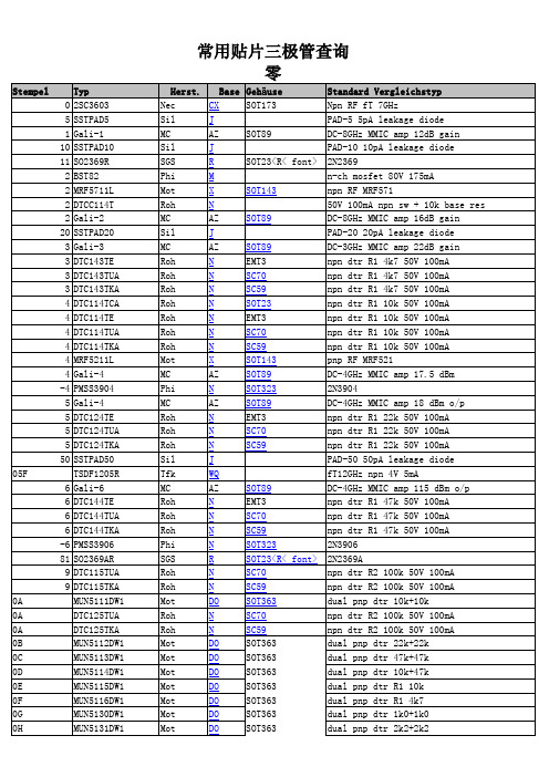
131 132 132 133 13A 13A 13E 13s 13s 13t 13V 13Y 13Y 14 14 14 14 14 142 14A 14s 14s 15 15 15 15 15 151 152 153 156 15A 15A 15s 15s 15V 15Y 16 16 16 161 162 163 166 16s 16s 16V 16Y 179 17s
BAS125-07W BFP181T PDTC143ZK PZM18NB1 PZM18NB2 PZM18NB3 PZM18NB BZV49-C18 BZV49-C18 PDTA143ZK DTA115EUA DTA115EKA Typ BC846 A PMBT3904 PXT3904 BC846A BC846AT FMMT3904 MMBT3904 IRLML2402 PMST3904 BC846AW MMBT3904L BC846A BC846A BC846AW PMBT2222 PXT2222 BC846 B BC846B BC846BT FMMT2222 MMBT2222 IRLML2803 PMST2222 BC846BW BC846B BC817UPN BC846B BC846BW FMMT-A20 MMBTA20L IRLML6302 BAP50-05 BC847S PMBTA42 BC846 MMBTA42
Sie Tfk Phi Phi Phi Phi Phi Phi Phi Rho Rho Herst.
S X N C C C C O N N N Base
Phi Phi Zet Mot IR Phi Phi Mot Phi Phi Phi
N N N N F N N N N N N
Phi Phi Zet Mot IR Phi Phi Phi Sie Phi Phi Zet Mot IR Phi Sie
74系列中文资料(超级全)
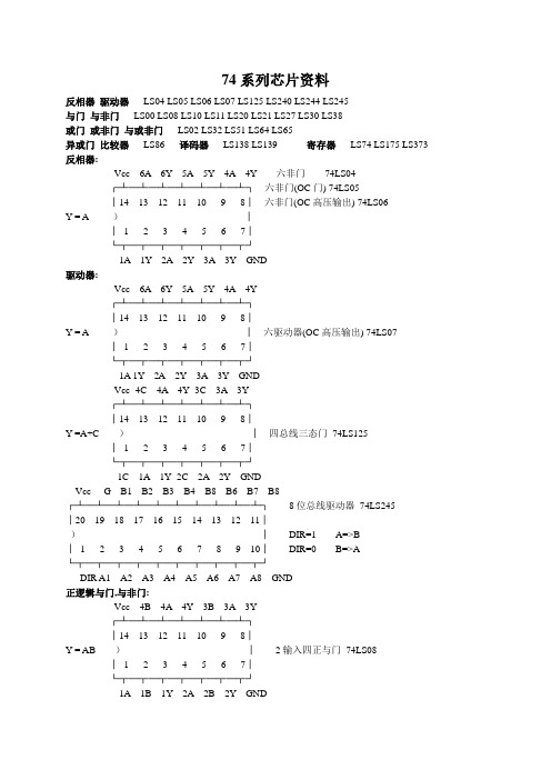
┌┴─┴─┴─┴─┴─┴─┴┐ 双 D 触发器 74LS74
│14 13 12 11 10 9 8 │
)
│
│ 1 2 3 4 5 6 7│
└┬─┬─┬─┬─┬─┬─┬┘
1Cr 1D 1Ck 1St 1Q -1Q GND
Vcc 8Q 8D 7D 7Q 6Q 6D 5D 5Q ALE
┌┴─┴─┴─┴─┴─┴─┴─┴─┴─┴┐ 8 位锁存器 74LS373
Vcc -G B1 B2 B3 B4 B8 B6 B7 B8
┌┴─┴─┴─┴─┴─┴─┴─┴─┴─┴┐ 8 位总线驱动器 74LS245
│20 19 18 17 16 15 14 13 12 11│
)
│ DIR=1 A=>B
│ 1 2 3 4 5 6 7 8 9 10│ DIR=0 B=>A
└┬─┬─┬─┬─┬─┬─┬─┬─┬─┬┘
___
)
│ Y = A+B
│ 1 2 3 4 5 6 7│
└┬─┬─┬─┬─┬─┬─┬┘
1Y 1A 1B 2Y 2A 2B GND
Vcc 2Y 2B 2A 2D 2E 1F
┌┴─┴─┴─┴─┴─┴─┴┐ 双与或非门 74S51
│14 13 12 11 10 9 8│
_____
)
│ 2Y = AB+DE
DIR A1 A2 A3 A4 A5 A6 A7 A8 GND
正逻辑与门,与非门:
Vcc 4B 4A 4Y 3B 3A 3Y
┌┴─┴─┴─┴─┴─┴─┴┐
│14 13 12 11 10 9 8│
Y = AB )
│ 2 输入四正与门 74LS08
│ 1 2 3 4 5 6 7│
- 1、下载文档前请自行甄别文档内容的完整性,平台不提供额外的编辑、内容补充、找答案等附加服务。
- 2、"仅部分预览"的文档,不可在线预览部分如存在完整性等问题,可反馈申请退款(可完整预览的文档不适用该条件!)。
- 3、如文档侵犯您的权益,请联系客服反馈,我们会尽快为您处理(人工客服工作时间:9:00-18:30)。
© 1999 Fairchild Semiconductor Corporation DS009501April 1988Revised July 199974F240 • 74F241 • 74F244 Octal Buffers/Line Drivers with 3-STATE Outputs74F240 • 74F241 • 74F244Octal Buffers/Line Drivers with 3-STATE OutputsGeneral DescriptionThe 74F240, 74F241 and 74F244 are octal buffers and line drivers designed to be employed as memory and address drivers, clock drivers and bus-oriented transmitters/receiv-ers which provide improved PC and board density.Featuress 3-STATE outputs drive bus lines or buffer memory address registers s Outputs sink 64 mA (48 mA mil)s 12 mA source currents Input clamp diodes limit high-speed termination effectsOrdering Code:Devices also available in T ape and Reel. Specify by appending the suffix letter “X” to the ordering code.Connection Diagrams74F24074F24174F244Order Code Package NumberPackage Description74F240SC M20B 20-Lead Small Outline Integrated Circuit (SOIC), JEDEC MS-013, 0.300 Wide 74F240SJ M20D 20-Lead Small Outline Package (SOP), EIAJ TYPE II, 5.3mm Wide 74F240PC N20A 20-Lead Plastic Dual-In-Line Package (PDIP), JEDEC MS-001, 0.300 Wide 74F241SC M20B 20-Lead Small Outline Integrated Circuit (SOIC), JEDEC MS-013, 0.300 Wide 74F241SJ M20D 20-Lead Small Outline Package (SOP), EIAJ TYPE II, 5.3mm Wide 74F241PC N20A 20-Lead Plastic Dual-In-Line Package (PDIP), JEDEC MS-001, 0.300 Wide 74F244SC M20B 20-Lead Small Outline Integrated Circuit (SOIC), JEDEC MS-013, 0.300 Wide 74F244SJ M20D 20-Lead Small Outline Package (SOP), EIAJ TYPE II, 5.3mm Wide 74F244MSA MSA2020-Lead Shrink Small Outline Package (SSOP), EIAJ TYPE II, 5.3mm Wide 74F244PCN20A20-Lead Plastic Dual-In-Line Package (PDIP), JEDEC MS-001, 0.300 Wide 274F 240 • 74F 241 • 74F 244Logic SymbolsIEEE/IEC 74F240IEEE/IEC 74F241IEEE/IEC 74F244Unit Loading/Fan OutNote 1: Worst-case 74F240 enabled; 74F241, 74F244 disabledTruth Tables74F24074F24174F244H = HIGH Voltage Level L = LOW Voltage Level X = ImmaterialZ = High ImpedancePin Names DescriptionU.L.Input I IH /I IL HIGH/LOW Output I OH /I OL OE 1, OE 23-STATE Output Enable Input (Active LOW) 1.0/1.66720 µA/−1 mA OE 23-STATE Output Enable Input (Active HIGH) 1.0/1.66720 µA/−1 mA I 0–I 7Inputs (74F240) 1.0/1.667 (Note 1)20 µA/−1 mA I 0–I 7Inputs (74F241, 74F244)1.0/2.667 (Note 1)20 µA/−1.6 mA O 0–O 7, O 0–O 7Outputs600/106.6 (80)−12 mA/64 mA (48 mA)OE 1D 1n O 1n OE 2D 2n O 2n H X Z H X Z L H L L H L LLH LLHOE 1D 1n O 1n OE 2D 2n O 2n H X Z L X Z L H H H H H LLLHLLOE 1D 1n O 1n OE 2D 2n O 2n H X Z H X Z L H H L H H LLLLLL74F240 • 74F241 • 74F244Absolute Maximum Ratings (Note 2)Recommended Operating ConditionsNote 2: Absolute maximum ratings are values beyond which the device may be damaged or have its useful life impaired. Functional operation under these conditions is not implied.Note 3: Either voltage limit or current limit is sufficient to protect inputs.DC Electrical CharacteristicsStorage Temperature−65°C to +150°C Ambient Temperature under Bias −55°C to +125°C Junction Temperature under Bias −55°C to +150°C V CC Pin Potential to Ground Pin −0.5V to +7.0V Input Voltage (Note 3)−0.5V to +7.0V Input Current (Note 3)−30 mA to +5.0 mAVoltage Applied to Output in HIGH State (with V CC = 0V)Standard Output −0.5V to V CC 3-STATE Output −0.5V to +5.5V Current Applied to Output in LOW State (Max)twice the rated I OL (mA)ESD Last Passing Voltage (Min)4000V Free Air Ambient Temperature 0°C to +70°C Supply Voltage+4.5V to +5.5VSymbol ParameterMin TypMaxUnits V CCConditionsV IH Input HIGH Voltage 2.0V Recognized as a HIGH Signal V IL Input LOW Voltage 0.8V Recognized as a LOW Signal V CD Input Clamp Diode Voltage −1.2VMin I IN = −18 mA V OHOutput HIGH 10% V CC 2.4VMinI OH = −3 mA Voltage10% V CC 2.0I OH = −15 mA 5% V CC 2.7I OH = −3 mA V OL Output LOW 10% V CC 0.55V Min I OL = 64 mA VoltageI IH Input HIGH 5.0µA Max V IN = 2.7V CurrentI BVI Input HIGH Current 7.0µA Max V IN = 7.0V Breakdown Test I CEX Output HIGH 50µA Max V OUT = V CC Leakage Current V ID Input Leakage 4.75V 0.0I ID = 1.9 µATestAll Other Pins Grounded I OD Output Leakage 3.75µA 0.0V IOD = 150 mVCircuit Current All Other Pins GroundedI IL Input LOW Current −1.0mAMaxV IN = 0.5V (OE 1, OE 2, OE 2, D n 74F240))−1.6V IN = 0.5V (D n (74F241, 74F244))I OZH Output Leakage Current 50µA Max V OUT = 2.7V I OZL Output Leakage Current −50µA Max V OUT = 0.5V I OS Output Short-Circuit Current −100−225mA Max V OUT = 0V I ZZ Bus Drainage Test500µA 0.0V V OUT = 5.25V I CCH Power Supply Current (74F240)1929mA Max V O = HIGH I CCL Power Supply Current (74F240)5075mA Max V O = LOW I CCZ Power Supply Current (74F240)4263mA Max V O = HIGH Z I CCH Power Supply Current 4060mA Max V O = HIGH (74F241, 74F244)I CCL Power Supply Current 6090mA Max V O = LOW (74F241, 74F244)I CCZPower Supply Current 6090mAMaxV O = HIGH Z(74F241, 74F244) 474F 240 • 74F 241 • 74F 244AC Electrical CharacteristicsSymbolParameterT A = +25°CT A = −55°C to +125°CT A = 0°C to +70°CUnitsV CC = +5.0V V CC = 5.0V V CC = 5.0V C L = 50 pFC L = 50 pF C L = 50 pF MinTyp Max Min Max Min Max t PLH Propagation Delay 3.0 5.17.0 3.09.0 3.08.0ns t PHL Data to Output (74F240) 2.0 3.5 4.7 2.0 6.0 2.0 5.7t PZH Output Enable Time (74F240)2.03.54.7 2.0 6.5 2.05.7ns t PZL 4.06.99.0 4.010.5 4.010.0t PHZ Output Disable Time (74F240) 2.0 4.0 5.3 2.0 6.5 2.0 6.3t PLZ 2.0 6.08.0 2.012.5 2.09.5t PLH Propagation Delay2.5 4.0 5.2 2.0 6.5 2.5 6.2ns t PHL Data to Output (74F241, 74F244) 2.5 4.0 5.2 2.07.0 2.5 6.5t PZH Output Enable Time 2.0 4.3 5.7 2.07.0 2.0 6.7ns t PZL (74F241, 74F244) 2.0 5.47.0 2.08.5 2.08.0t PHZ Output Disable Time 2.0 4.5 6.0 2.07.0 2.07.0t PLZ(74F241, 74F244)2.04.56.02.07.52.07.074F240 • 74F241 • 74F244Physical Dimensions inches (millimeters) unless otherwise noted20-Lead Small Outline Integrated Circuit (SOIC), JEDEC MS-013, 0.300 WidePackage Number M20B20-Lead Small Outline Package (SOP), EIAJ TYPE II, 5.3mm WidePackage Number M20D 674F 240 • 74F 241 • 74F 244Physical Dimensions inches (millimeters) unless otherwise noted (Continued)20-Lead Shrink Small Outline Package (SSOP), EIAJ TYPE II, 5.3mm WidePackage Number MSA20774F240 • 74F241 • 74F244 Octal Buffers/Line Drivers with 3-STATE OutputsPhysical Dimensions inches (millimeters) unless otherwise noted (Continued)20-Lead Plastic Dual-In-Line Package (PDIP), JEDEC MS-001, 0.300 WidePackage Number N20AFairchild does not assume any responsibility for use of any circuitry described, no circuit patent licenses are implied and Fairchild reserves the right at any time without notice to change said circuitry and specifications.LIFE SUPPORT POLICYFAIRCHILD’S PRODUCTS ARE NOT AUTHORIZED FOR USE AS CRITICAL COMPONENTS IN LIFE SUPPORT DEVICES OR SYSTEMS WITHOUT THE EXPRESS WRITTEN APPROVAL OF THE PRESIDENT OF FAIRCHILD SEMICONDUCTOR CORPORATION. As used herein:1.Life support devices or systems are devices or systems which, (a) are intended for surgical implant into the body, or (b) support or sustain life, and (c) whose failure to perform when properly used in accordance with instructions for use provided in the labeling, can be rea-sonably expected to result in a significant injury to the user.2. A critical component in any component of a life support device or system whose failure to perform can be rea-sonably expected to cause the failure of the life support device or system, or to affect its safety or effectiveness.。