MAX6832VXRD0-T中文资料
AXOS系列产品简介说明书

EMC TESTING PRODUCT OVERVIEWCUSTOMER BASE FOR EMC TESTINGCOMPACT TESTERThe AXOS is an ultra-compact immunity tester that performs all the most commonly used transient immunity tests, including Surge, EFT, Dips/Interrupts, AC/Surge Magnetic Field, Ring Wave and Telecom Surge. Full Compliance and Pre-Compliance tests are performed to meet the requirements of a wide variety of transient immunity standards, including IEC 61000-4-x “CE Mark” Basic standards, IEC 60601 for Medical equipment, and many other IEC, ANSI, ITU, UL and specific product standards.P C D 126AD E C 5D E C 6D E C 7I P 4BP A T 50 AP A T 1000Surge 1.2/50 & 8/20, 5.0kV EFT / Burst 5.0kV Dips & InterruptsSurge magnetic field 61000-4-9Insulation testing 1.2/50, 15kV 3-phase surge 32A 3-phase surge 100A 3-phase EFT/Burst 32A 3-phase EFT/Burst 100ACDNs symmetrical data & control lines CDNs asymmetrical data & control lines Capacitive coupling clampsELECTROSTATIC DISCHARGEThe ONYX simulators by HAEFELY HIPOTRONICS have been specially designed to meet all latest international standards, including IEC61000-4-2 Ed. 2 and are the most ergonomic battery and AC power operated 30kV guns on the market. 16kV and 30kV models available, along with a complete range of accessories that ensure a complete ESD test setup (verification equipment, test tables, coupling planes etc).FEATURESSTANDARDS a 16kV and 30kV models a Touch screen operation a Modulara Automatic polarity switching a Remote control software a Remote triggera Bleed-of Functionalitya Lightweight and portable design a Battery and AC operation a Environmental monitoring a Onboard LED EUT light a Smart key functionsa Contact discharge current flow detection a Self-test functiona IEC 61000-4-2 Ed. 2a IEC613402-1/-2a IEC 801-2a IEC 60571a EN 50155 a ANSI C63.16a ISO 10605a ISO 14304a ITU-T K20a MIL-STD-1512/-1514/-750D/-883a RTCA/DO-160a JEDEC 22-A114A a GR-78/1089-COREThe self test function is a built-in self test routine which checks the HV supply, the impulse capacitor, the HV discharge relays, and the insulation of the entire HV circuitry.Bleed-off functionalityThe so called bleed-off functionality of the ONYX simulator ensures via an integrated relay that the EUT is completely discharged before the next ESD pulse is initiated. This functionality ensures a maximum of test accuracy to the user without the need for a discharge brush.Smart Key OperationThe smart key button is integrated at the upper part of the discharge trigger and has various functions which are defined by the user, enabling you to run a sequence of events according to your testing requirements, and simplify test procedures.The functions include user defined discharge voltages steps, sweep voltage, On/Off LED light, Polarity Switching, control and report function.Compliance & ModularityThe design is based on the requirements of all latest international standards, including the latest IEC 61000-4-2 Ed. 2. R/C module values are available from 50-5000 Ohms and 50-1000pF , which enables users to fully test according to many international standards.Contact Discharge Current Flow Detection & Self T estThe unique NO CONTACT detection circuit function continuously monitors whether ESD pulses are discharged to the EUT , ensures users the test was successful and prevents incorrect test results.ONYX 16n16kV Electrostatic Discharge Simulatorn16kV Air & Contact Dischargen150pF/330Ω standard discharge networkn Exchangeable RC modules to meet variousstandard requirements (IEC, ISO, ANSI, MIL)n Ergonomic design and operation (touch screen) n Rechargeable battery or mains operatedn Smart key functionsn Automatic polarity switchingn Remote triggern Self test functionn Includes: Light rigid carrying case, contact and air discharge tips, mains supply, 2 x rechargeable battery pack with chargerSOFTWAREWhy should you use software to perform ESD tests?Because it makes your life easier and helps to make tests more reliable and reproducible. Benefitsn Windows XP, Windows Vista and Windows 7 compatibilityn Support of USB and optical USB interfacesn Easy-to-use and intuitive creator for test plans and test proceduresn Enhanced and highly flexible reporting capabilitiesn Up-to-date design and navigationn Intuitive operationn Independent test station n High end componentsn Very high result accuracy and precision n Higher voltage level of 7.3kV n Spike frequency up to 110 kHz n IEC/EN61000-4-4 Ed. 3n Unique windows based control and reporting software n Distinctive safety features n Ideal for over testingn Multi-test stationn Covers EFT/Burst, Surge, Dips & Interrupts, Magnetic Field, and Insulation Tests n 5.0kV EFT/Burstn Fully meets all latest standards including IEC/EN61000-4-4 Ed. 3n Ideal for pre-compliance testing and CE markingNOTE: Please refer to the COMPACT section on page 3 for details.All our EFT/Burst generators are 100% compliant to the latest standards, including IEC/EN 61000-4-4 Ed. 3, which is mandatory from April 2012.DISTINCTIVE FEATURESSTAND-ALONECOMPACTEFT/BURSTBursts or EFTs (Electrical Fast Transients) are caused by operation of electro-mechanical switches, motors and distribution switch-gear connected to the power distribution network. A typical burst consists of a large number of recurring impulses at high frequency for a short time period.V 90%50%10%FlexibilityDepending on the actual testing requirements, we offer our customers the choice between stand alone and compact testing equipment.Stand alone equipment allow users to test at levels higher than what is usually required within the standards, making such testers ideal for over-testing purposes.Compact solutions allow users to not only cover the latest eft/burst requirements, but also to carry out surge, dips & interrupts, magnetic field, and insulation tests.EFT SOLUTIONSn 5kV Burst Test Systemn Built according to IEC/EN 61000-4-4 Ed. 2 & 3 as well as to ANSI/IEEE C62.41/45 and C37.90.1n Impulse voltage up to 5kVn Frequency range from 1Hz to 1MHzn IEC, random, continuous and real burst mode n Ramp functionsn Integrated automated single-phase CDN for AC and DC up to 16A EUT mains current n Burst parameters editable during testingn 7.3kV Burst Test Systemn Built according to IEC/EN 61000-4-4 Ed. 2 & 3 as well as to ANSI/IEEE C62.41/45 and C37.90.1n Impulse voltage up to 7.3kVn Frequency range from 1Hz to 100kHzn IEC, random, continuous and real burst mode n Ramp functionsn Integrated automated single-phase CDN for AC and DC up to 16A EUT mains current n Burst parameters editable during testingAXOS SERIESPEFT 8010MANUAL 32A THREE-PHASE COUPLING-DECOUPLING NETWORK FOR EFT TESTING100A THREE-PHASE COUPLING/DECOUPLING NET-WORK FOR EFT TESTINGFP-EFT 32MFP-EFT 100M2n Built according to IEC/EN 61000-4-4 Ed. 2 & 3 and ANSI C62.41/45n Superposition of EFT impulses onto three- phase power lines and DC power lines n 8kV maximum impulse voltage n EUT voltage up to 690V/400V ACn EUT mains current up to 100A per phase n Manual coupling path switchingnSynchronization with power supply possiblen Built according to IEC/EN 61000-4-4 Ed. 2 & 3 as well as to ANSI C62.41/45n Superposition of EFT impulses onto three- phase power lines and DC power linesn 8kV maximum impulse voltagen EUT mains voltage up to 690V/400V AC, 110V DC n EUT mains current up to 32A per phase n Synchronization with power supply possible nEUT over-current protectionEFT VERIFICATION SETWAVEFORM VERIFICATION SETOPTIONSn Built according to IEC/EN 61000-4-4 Ed. 2 & 3 and ANSI C37.90.1n 40mm maximum cable size n Up to 8kV impulse voltage n Handy carrying handlen Optional transducer plate for clamp calibration/ verificationn Built according to IEC/EN 61000-4-4 Ed. 2 & 3n For verification/calibration of EFT generators (PEFT 4010, PEFT 8010, AXOS Series)n Combined 50Ω load, 54 dB attenuator n Combined 1 k Ω load, 60 dB attenuator n Required cables includedn Supplied with detailed application noten IEEE 488 interface optionn Three phase verification adaptersn Warning lamps and emergency switches n Fibre optic links (EUT fail)n Test tablesn Dedicated software WinFEAT&R n Upgrade kits for older modelsnReal burst functional extensionn Optical decoupling fibre optic links (RS232)n AC and DC adaptersn Near field test probes (E&H)n Vertical operation stands VOSSURGE - TRANSIENT / LIGHTNINGPRODUCTS AND APPLICATIONSStand-alone, compact, and modular Surge impulse generators are available up to 30kV , which cover a range of EMC surge tests including the classical IEC defined “Combination Wave“ 1.2/50 & 8/20, “Hybrid waves“ defined for telecommunications testing, 10/700, ring wave, damped oscillating wave, magnetic field, and many more.Typical standard applications include IEC, EN and ANSI for power line testing, FCC, Bellcore, ITU and ETSI for telecom testing.Our modular Surge Platform can also be used for product safety testing to UL standards and also ITE requirements. A wide range of accessories from single and three phase CDNs up to 100A and telecoms coupling units, make these systems the most modular and flexible test equipment on themarket.32A THREE-PHASE COUPLING/DECOUPLING NETWORK FOR SURGE TESTINGFP-COMB 32n Built according to IEC/EN 61000-4-5 Ed. 2 & 3n EUT voltage up to 480Vn EUT current up to 32A per phasenTest level max. 7.0kV / 3.5kA n Fully automatic test routinesn Automatic synch source switching n Test object power line bypass mode n Test object overcurrent protection15KV VOLTAGE SURGE GENERATORPS 1500n Built according to IEC/EN 60065,IEC/EN 60950-1 and UL 1414n Impulse voltage up to 15kV n Up to 24 discharges per minute n Positive and Negative Polarity n External trigger inputn Automatic selection of 4M Ω/100 M Ω parallel resistor n Impulse voltage monitor n Includes test pistol n Flash measurement n Insulation/safety testing n Component testingn Small and compact design30KV SURGE TEST SYSTEMSINGLE-PHASE COUPLING/DECOUPLING NETWORKFOR SURGE TESTING UP TO 30KV / 15KAPSURGE 30.2FP-SURGE 3010n Single-phase EUT powering n EUT mains voltage up to 480V n EUT mains current up to 10An Manual selection of coupling path and coupling capacitor n Test level up to 15kV/30kA n EUT overcurrent protection n Large integrated test cabinetn Built according to IEC/EN61000-4-5, IEC/EN 61010, IEC/EN 61643-1 and ANSI C62.41/45n Impulse voltage up to 30kV (combination wave)n Impulse current up to 30kA (8/20 µs)n Combination wave (1.2/50 µs & 8/20 µs)n 8/20 µs, 10/350 µs, 10/1000 µs current pulse n Impulse voltage & current measurement n Automatic polarity switching n Integrated test cabinetPIM 100PIM 110COMBINATION WAVE IMPULSE MODULERING WAVE IMPULSE MODULEn Built according to IEC/EN 61000-4-5 Ed. 1 & 2 and ANSI C62.41/45n 1.2/50 µs open circuit up to 7.4kV n 8/20 µs short circuit up to 3.7kAnImpulse voltage and current monitors n *1° Phase synchronizationn Reliable semiconductor HV-switchn Positive, negative and alternating polarity n Up to 12 pulses per minuten Built according to IEC/EN 61000-4-12 and ANSI C62.41/45n 100 kHz frequency, 0.5 µs rise time n Imp. voltage up to 7.8kV / 12 Ω, 30 Ω and 200 Ωn Impulse voltage and current monitors n *1° phase synchronizationn Positive, negative and alternating polarity n Up to 12 pulses per minuten Reliable semiconductor HV-switch100A THREE-PHASE COUPLING/DECOUPLING NETWORKMANUAL SURGE COUPLING UNIT FOR SYMMETRICAL DATA AND CONTROL LINESPCD 121n Built according to IEC/EN 61000-4-5 Ed. 2 Fig. 14 & Ed. 3 Fig. 10n Coupling of Combination Wave impulses n Up to 2 pairs / 4 wires can be testedn Serial resistors included, 4 x 40/80/160 Ohm n Gas arrestors and Avalanche Breakdown Diodes coupling elements included n Can be used with any surge generator n Impulse voltage up to 6.6kVnSignal Bandwidth up to > 10 MHzPCD 122MANUAL SURGE COUPLING UNIT FOR SYMMETRICAL DATA AND CONTROL LINESn Built according to IEC/EN 61000-4-5 Ed. 2 Fig. 14 & Ed. 3 Fig. 10n Coupling of 10/700 µs impulsesn Up to 2 pairs / 4 wires can be testedn Serial resistors included, 4 x 25/50/100 Ohmn Gas arrestors and Avalanche Breakdown Diodes coupling elements included n Can be used with any surge generator n Impulse voltage up to 6.6kVn Signal Bandwidth up to > 10 MHz.MANUAL SURGE COUPLING/DECOUPLING UNIT FOR DATA AND SURGE DECOUPLING UNIT FOR SYMMETRICAL DATAn Signal Bandwidth up to some 10MHzDEC 7SURGE DECOUPLING UNIT FOR ASYMMETRICAL DATA AND CONTROL LINESn Built according to:IEC/EN 61000-4-5 Ed. 2 Fig. 11, 12 & 13 & Ed. 3 Fig. 9IEC 61000-4-12:1995 Fig. 9, 10, 13 & 14 Array n Decoupling of Combination wave impulsesn Decoupling of Ring Wave (100kHz) impulsesn Up to four wire can be tested simultaneousn Decoupling: Inductors 20mH not compensatedn Protection elements are Varistors and Breakdown avalanche diodesn Can be used with any surge generatorn Impulse voltage up to 6.6kVn Signal Bandwidth up to some 100 HzLOW ENERGY IMPULSE TRANSFORMER FOR INSULATION TESTING NETWORK FOR SURGE PLATFORMPOWER FREQUENCY MAGNETIC FIELD TEST SYSTEMMAG 1000n Built according to IEC/EN 61000-4-8n 1m x 1m antenna included w/ stand n Up to 1100A/m field strength n Horizontal and Vertical testingn Continuous and short duration testing n Built in power supply at 50/60Hz n Simple interfaceMSURGE-APULSE MAGNETIC FIELD TEST SYSTEMnBuilt according to IEC/EN 61000-4-9n 8/20µs magnetic field wave shape n Up to 3000A/m field strength n Sturdy constructionn Horizontal and vertical testingn Control from HAEFEL Y surge generators n Single turn coil with 1m x 1m square area n Optional 2m x 2.6m magnetic coilDip: decrease of the mains VoltageSOFTWAREThe WinFEAT&R software is the latest generation of control and reporting software, based on a modern Drag and Drop concept. With such ease of use, even users with minimum technical experience will be carrying out tests in no time.This unique software allows users to run user specified or pre-defined tests according to the latest standards, and monitors and displays real time output current and voltage values.Communication between software and oscilloscope monitoring allows screenshots to be added to the test report.The software runs up to Windows 7 and is compatible with all stand-alone HAEFEL Y HIPOTRONICS test generators.FEATURESn Control and reporting for stand-alone EFT/Burst, Surge, Dips& Interrupts generators.n Drag and Drop applicationn User defined tests can be added and pre-defined tests arealready included (according to the standards).n Output Current/Voltage monitoring during test.n EUT supervision (max/min V/I levels).n User friendly, designed for use by users with minimumtechnical experience.n Automatic synchronization between software and PC.n Test setup uploaded to Oscilloscope.n User defined test report with oscilloscope screenshotoption.n Fully compatible with Windows 7 (32-bit/64-bit)A u g u s t 2013EuropeChinaNorth America Haefely T est AG Haefely T est AG Representative Beijing OfficeHipotronics, Inc.Birsstrasse 300 8-1-602, Fortune Street1650 Route 22 N 4052 Basel No. 67, Chaoyang Road, Chaoyang DistrictBrewster, NY 10509SwitzerlandBeijing, China 100025United States☎ + 41 61 373 4111 ☎ +86 10 8578 8099 ☎ +1 845 230 9245 + 41 61 373 4912+86 10 8578 9908 +1 845 279 2467emc-**********************************.cn*********************HAEFEL Y HIPOTRONICS has a policy of continuous product improvement. We therefore reserve the right to change design and specification without notice.OFFICES:。
SD6832PDF规格说明书
为减小在上电过程中变压器的应力,防止变压器饱和,上电时,峰值电流补偿最大,然后逐渐达到平 衡。达到平衡的时间随负载而定。
测试条件 VGS=0V,ID=50μA VDS=650V,VGS=0V VDS=480V,VGS=0V Tamb=125°C VGS=10V,ID=0.5A VGS=0V,VDS=25V,f=1MHz VGS=0V,VDS=25V,f=1MHz VGS=0V,VDS=25V,f=1MHz VDD=0.5BVDSS ,ID=25mA VDD=0.5BVDSS ,ID=25mA VDD=0.5BVDSS ,ID=25mA VDD=0.5BVDSS ,ID=25mA
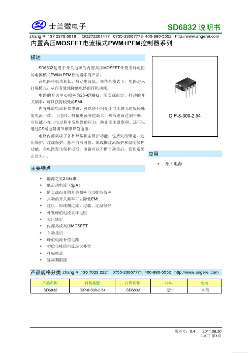
SD6832 说明书
zhang R 137 2378 6618 QQ272261417 0755-33067773 400-880-5552
内置高压MOSFET电流模式PWM+PFM控制器系列
描述
SD6832是用于开关电源的内置高压MOSFET外置采样电阻
2. 频率抖动和降频模式
为了降低 EMI,本电路使得振荡频率不断的变化,减小在某一个单一频率的对外辐射。振荡频率在一个 很小的范围内变动,从而简化 EMI 设计,更容易满足要求。中心频率 67KHz 时变化的规律是:4ms 时间之 内±2.5KHz 范围变化,共有 63 个频率点。
为提高效率,本电路采用降频模式。采用方式有二: 一、 通过检测 FB 管脚输出下拉电流 IFB 来降低频率 f。当 IFB 在典型电流 I1 以上时,频率 f 从典型值 67KHz
MEMORY存储芯片MAX660ESA+T中文规格书

MAX660 CMOS Monolithic Voltage ConverterM A X 660CMOS Monolithic Voltage Converter ______________Detailed DescriptionThe MAX660 capacitive charge-pump circuit eitherinverts or doubles the input voltage (see TypicalOperating Circuits ). For highest performance, loweffective series resistance (ESR) capacitors should beused. See Capacitor Selection section for more details.When using the inverting mode with a supply voltageless than 3V, LV must be connected to G ND. Thisbypasses the internal regulator circuitry and providesbest performance in low-voltage applications. Whenusing the inverter mode with a supply voltage above3V, LV may be connected to GND or left open. The partis typically operated with LV grounded, but since LVmay be left open, the substitution of the MAX660 for theICL7660 is simplified. LV must be grounded when over-driving OSC (see Changing Oscillator Frequency sec-tion). Connect LV to OUT (for any supply voltage) whenusing the doubling mode.__________Applications InformationNegative Voltage ConverterThe most common application of the MAX660 is as acharge-pump voltage inverter. The operating circuituses only two external capacitors, C1 and C2 (seeTypical Operating Circuits ).Even though its output is not actively regulated, theMAX660 is very insensitive to load current changes. Atypical output source resistance of 6.5Ωmeans thatwith an input of +5V the output voltage is -5V underlight load, and decreases only to -4.35V with a load of100mA. Output source resistance vs. temperature andsupply voltage are shown in the T ypical OperatingCharacteristics graphs.Output ripple voltage is calculated by noting the outputcurrent supplied is solely from capacitor C2 during one-half of the charge-pump cycle. This introduces a peak-to-peak ripple of:V RIPPLE = I OUT +I OUT (ESR C2)2(f PUMP ) (C2)For a nominal f PUMP of 5kHz (one-half the nominal 10kHz oscillator frequency) and C2 = 150µF with an ESR of 0.2Ω, ripple is approximately 90mV with a 100mA load current. If C2 is raised to 390µF, the ripple drops to 45mV.Positive Voltage Doubler The MAX660 operates in the voltage-doubling mode as shown in the T ypical Operating Circuit.The no-load output is 2 x V IN .Other Switched-Capacitor Converters Please refer to Table 1, which shows Maxim’s charge-pump offerings.Changing Oscillator Frequency Four modes control the MAX660’s clock frequency, as listed below:FC OSC Oscillator Frequency Open Open 10kHz FC = V+Open 80kHz Open or External See Typical Operating FC = V+Capacitor Characteristics Open External External Clock Frequency Clock When FC and OSC are unconnected (open), the oscil-lator runs at 10kHz typically. When FC is connected to V+, the charge and discharge current at OSC changes from 1.0µA to 8.0µA, thus increasing the oscillatorTable 1. Single-Output Charge Pumps。
MEMORY存储芯片MAX208CWG+T中文规格书

Detailed Description The MAX200–MAX209/MAX211/MAX213 consist of three sections: charge-pump voltage converters, drivers (trans-mitters), and receivers. Each section is described in detail.+5V to ±10V Dual Charge-Pump Voltage Converter The +5V to ±10V conversion is performed by two charge-pump voltage converters (Figure 4). The first uses capaci-tor C1 to double +5V to +10V, storing +10V on the V+output filter capacitor, C3. The second chargepump volt-age converter uses capacitor C2 to invert +10V to -10V,storing -10V on the V- output filter capacitor, C4.The MAX201 and MAX209 include only the V+ to Vcharge pump, and are intended for applications that have a V CC = +5V supply and a V+ supply in the +9V to +13.2V range.In shutdown mode, V+ is internally connected to V CC by a 1kΩ pulldown resistor and V- is internally connected to ground by a 1kΩ pullup resistor.RS-232 Drivers When V CC = +5V, the typical driver output-voltage swing is ±8V when loaded with a nominal 5kΩ RS-232 receiver. The output swing is guaranteed to meet the EIA/TIA-232E and V.28 specifications, which call for ±5V minimum out-put levels under worst-case conditions. These include a minimum 3kΩ load, V CC = +4.5V, and the maximum operating temperature. The open-circuit output-voltage swing ranges from (V+ - 0.6V) to V-.Input thresholds are both CMOS and TTL compatible. The inputs of unused drivers can be left unconnected since 400kΩ pullup resistors to V CC are included onchip. Since all drivers invert, the pullup resistors force the outputs of unused drivers low. The input pullup resistors typically source 15μA; therefore, the driver inputs should be driven high or open circuited to minimize power-supply current in shutdown mode.When in low-power shutdown mode, the driver outputs are turned off and their leakage current is less than 1mA, even if the transmitter output is backdriven between 0V and (V CC + 6V). Below -0.5V, the transmitter output is diode clamped to ground with a 1kΩ series impedance. The transmitter output is also zener clamped to approxi-mately (V CC + 6V), with a 1kΩ series impedance.Figure 1. Shutdown Current Test CircuitFigure 2. Receiver Output Enable and Disable Timing Integrated │ 5找MEMORY 、二三极管上美光存储Applications InformationCapacitor SelectionThe type of capacitor used is not critical for properoperation. Ceramic capacitors are suggested. To ensureproper RS-232 signal levels over temperature whenusing 0.1µF capacitors, make sure the capacitance valuedoes not degrade excessively as the temperature varies.If in doubt, use capacitors with a larger nominal value.Also observe the capacitors’ ESR value over tempera-ture, since it influences the amount of ripple on V+ andV-. To reduce the output impedance at V+ and V-, uselarger capacitors (up to 10µF). If polarized capacitors areused, obey the polarities shown in Figure 1 and the pinconfigurations.Driving Multiple ReceiversEach transmitter is designed to drive a single receiver.Transmitters can be paralleled to drive multiple receivers.Driver Outputs When Exiting Shutdown Figure 5 shows two driver outputs exiting shutdown. As they become active, the two driver outputs go to opposite RS-232 levels (one driver input is high, the other is low). Each driver is loaded with 3kΩ in parallel with 2500pF. The driver outputs display no ringing or undesirable tran-sients as they come out of shutdown.Power-Supply Decoupling In applications that are sensitive to power-supply noise, decouple V CC to ground with a capacitor of the same value as the charge-pump capacitors.V+ and V- as Power Supplies A small amount of power can be drawn from V+ and V-,although this reduces noise margins.Power Supplies for MAX201/MAX209If at power-up the V+ supply rises after the V CC supply,place a diode (e.g., 1N914) in series with the V+ supply.Table 2. Summary of EIA/TIA-232E, V.28 SpecificationsTable 3. DB9 Cable Connections Commonly Used for EIA/TIA-232E and V.24 Asynchronous InterfacesPARAMETERCONDITION EIA/TIA-232E, V.28 SPECIFICATION Driver Output Voltage: 0 Level3kΩ to 7kΩ load +5.0V to +15V Driver Output Voltage: 1 Level3kΩ to 7kΩ load -5.0V to -15V Output Level, MaximumNo load ±25V Data Rate3kΩ ≤ R L ≤ 7kΩ, C L ≤ 2500pF Up to 20kbps Receiver Input Voltage: 0 Level—+3.0V to +15V Receiver Input Voltage: 1 Level—-3.0V to -15V Input Level, Maximum—±25V Instantaneous Slew Rate, Maximum3kΩ ≤ R L ≤ 7kΩ, C L ≤ 2500pF 30V/µs Driver Output Short-Circuit Current, Maximum—100mA Transition Rate on Driver OutputV.281ms or 3% of the period EIA/TIA-232E 4% of the period Driver Output Resistance -2V < V OUT < +2V 300ΩPINNAME CONNECTION 1Received Line Signal Detector, sometimes called Carrier Detect (DCD)Handshake from DCE 2Receive Data (RD)Data from DCE 3Transmit Data (TD)Data from DTE 4Data Terminal Ready Handshake from DTE 5Signal Ground Reference point for signals 6Data Set Ready (DSR)Handshake from DCE 7Request to Send (RTS)Handshake from DTE 8Clear to Send (CTS)Handshake from DCE 9Ring Indicator Handshake from DCEMAX200–MAX209/MAX211/MAX213+5V, RS-232 Transceivers with 0.1μF External Capacitors Integrated │ 8。
SD6830资料
1. DescriptionSD6830 is a remote control transmitter, consists of the optimized 4-bit CPU with ROM and RAM. It contains power-on reset, watchdog timer and carrier frequency generator. The SD6830 provide a various carrier frequency for encoding output of key matrix and has built-in transistor to drive infrared LED. The SD6830 is supported with a software development tool, which allows code development in a PC environment. It allows the user to simulate the SD6830 on an instruction level.2. Features• Number of basic instructions ------------------------------------- 45 • Instruction cycle time (one word instruction)At Fsys=480KHz ---------------------------------------- 16.67uS At Fsys=455kHz ---------------------------------------- 17.58uS • Memory sizeROM --------------------------------------------------- 1024 x 8 Bits RAM ------------------------------------------------------ 32 x 4 Bits • Input ports (D0 ~ D3, E0 ~ E3 : with pull-up resistor) • Output ports (C, G, K, F0 ~ F7) • Carrier frequency generatorFsys/12 (1/2 duty), Fsys/12 (1/3 duty), Fsys/12 (1/4 duty),Fsys/8 (1/2 duty), Fsys/8 (1/4 duty), Fsys/11 (4/11 duty), No carrier • Watchdog Timer• Built-in power on reset• Single power supply ------------------------------------------------ 1.8V ~ 3.6V • Power dissipation (stop mode , VDD = 3V) ----------------------- Less than 3uW• Package ------------------------------------------------------------- 20/24 DIP, 20/24 SOP • Low-power system applications such as an infrared remote controller• MASK OPTION1. Divide ratio of the oscillator frequency2. Whether connected infrared LED driver or not * Descriptions of this spec sheet assume that the SD6830 include driver for infrared LED.3. Ordering InformationType NO.Marking Package CodeSD6830P-option SD6830P-option DIP20SD6830-option SD6830-option SOP20SD6830P-option SD6830P-option DIP24SD6830-optionSD6830-optionSOP24SD68304BIT MICROCONTROLLERS e m i c o n d u c t o r4. Block DiagramFigure 4-1 Block Diagram of the SD68305. PIN Assignment and Description5.1 PIN Assignment for 24PINS( DIP24, SOP24)Figure 5-1. Pin Assignment of 24 Pins5.2 PIN Description for 24 PINSSymbolPin No.I /OFunctions I/O TypeVDD 24-Power Supply VSS 1-GroundTEST 22INPUT Input for test ( Normally connected to VSS )OSCin 2INPUT Input for oscillating OSCout 3OUTPUT Output for oscillatingC/REM 23OUTPUT 1-Bit output for remote transmissionB D0 - D3 5 ~ 8INPUT 4-Bit input for key sense ( with pull-up resistor )A E0 - E39 ~ 12INPUT 4-Bit input for key sense ( with pull-up resistor )A F0 - F720 ~ 13OUTPUT 1-Bit individual output for key scan C G 4OUTPUT 1-Bit output D K21OUTPUT1-Bit outputD5.3 PIN Assignment for 20PINS( DIP20, SOP20)Figure 5-3. Pin Assignment of 20Pin5.4 PIN Description for 20 PINSSymbolPin No.I /OFunctions I/O TypeVDD 20-Power Supply VSS 1-GroundTEST 18INPUT Input for test ( Normally connected to VSS )OSCin 2INPUT Input for oscillating OSCout 3OUTPUT Output for oscillatingC/REM 19OUTPUT 1-Bit output for remote transmissionB D0 - D3 4 ~ 7INPUT 4-Bit input for key scan ( with pull-up resistor )A E0 – E18 ~ 9INPUT 2-Bit input for key scan ( with pull-up resistor )A F0 – F616 ~ 10OUTPUT 1-Bit individual output for key scan C K17OUTPUT1-Bit outputD5.5 I/O CIRCUIT SCHEMATICSFigure 5-5. I/O Circuit SchematicsNOTE : If STOP mode is specified, the TYPE C output becomes "L" state and the TYPE B output becomes floating state, the TYPE D output maintains previous state.ΤΨΠΕ ΑΤΨΠΕ ΒΤΨΠΕ ∆ΤΨΠΕ ΧNote : If STOP mode is specified, the TYPE C output becomes “L” state and the TYPE B output becomes floating state, the TYPE D output maintains previous state6. Basic Function Block6.1 Program Counter (PC)Program counter is used to indicate the address of the next instruction to be executed.The 10-bit program counter consists of two registers, PCH (4-bit) and PCL(6-bit).This is a polynomial counter.6.2 Program Memory (ROM)Program memory is used to store user-specified program. This consists of a 1024 x 8-bit.It is organized in 16 pages and each page is 64 bytes long. For page-in addressing, all instructions excluding JMPL and CALL can be executed by page. In order to execute jump or call in page, JMP or CAL is suitable. For page-to-page addressing, JMPL or CALL must be used.6.3 Data Memory (RAM)Data memory is used to store various type of processing data. This consists of a 32-nibble, which is organized into two files of 16 nibbles each. RAM addressing is indirectly implemented by a two registers; H, L. It’s upper 1-bit register (H) selects one of two files and its lower 4-bit register (L) selects one of 16 nibbles in the selected file.Figure 6-2. Data Memory Map6.4 Stack Register (SK)Stack register is used to store return address and provide a particularly mechanism for transferring control between programs. Two level hardware push/pop stacks are manipulated by CAL, CALL, and RET instructions. CAL/CALL instructions push the current program counter value, incremented by “1”, into stack level 1. Stack level 1 is automatically pushed to level 2.If more than two subsequent CAL/CALL are executed, only the most recent two return addresses are stored. RET instruction load the contents of stack level 1 into the program counter while stack level 2 gets copied into level 1. If more than two subsequent RET are executed, the stack will be filled with the address previously stored in level 2.6.5 Arithmetic and Logic Unit (ALU)This unit is used to perform arithmetic and logical operations such as addition, comparison, and bit manipulation.6.6 Carry Flag (CY)The carry flag contains the carry generated by the arithmetic and logical unit immediately after an operation. The set carry (SETB CY) and clear carry (CLRB CY) instructions allow direct access for setting and clearing this flag.6.7 Skip Flag (SF)The skip flag is a 1-bit register, which enables programs to conditionally skip an instruction. All instructions are executed when this flag is , the program executes NOP instruction and resets SF to “0”. Then program execution proceeds.The following instructions affect the skip flagInstructions Set conditions of SFArithmeticADD nINC LIf carry occurs(L) = 0CompareIF0 @HL.bIF0 CYIFEQU @HLIFEQU nM[HL].b = 0(CY) = 0(A) = M[HL].b(A) = nData Transfer STA @HL+XCH @HL+(L) = 0(L) = 0The instructions, which doesn t affect the skip flag but have a skip condition, are as follows.Instructions Skip conditionsData Transfer LDA nLDL nIf it is continuous, skip next sameinstruction.If it is continuous, skip next sameinstruction.Bit Manipulate SETB HCLRB HIf SETB H or CLRB H are continuous,skip nextSETB H or CLRB H instruction.6.8 RegistersRegister ARegister A, called the accumulator, plays a central role, is used to store an input or an output operand (result) in the execution of most instructions. It consists of 4-bit.Register BRegister B is used to store a temporary data in CPU. It consists of 4-bit.Register HRegister H is used to indicate an address of the data memory in conjunction with register L. It consists of 1-bit, which is related with the bit 0 of accumulatorRegister LRegister L is used to indicate an address of the data memory in conjunction with register H, Also lower 3-bit can be used to indicate the bit position of the port F. It consists of 4-bitRegister ZRegister Z is used to select a carrier frequency. The carrier frequency must be selected before Port C data write operation. It consists of 3-bit.Register ZCarrier frequencyBit 2Bit 1Bit 0/12, 1/2 duty000FSYS001F/12, 1/3 dutySYS/12, 1/4 duty010FSYS/8, 1/2 duty011FSYS100F/8, 1/4 dutySYS/11, 4/11 duty101FSYS110 No carrier111 No carrier6.9 I /O PortsPort C/REMPort C/REM is a 1-bit output port, which is related with the bit 3 of accumulator, with CMOS N-channel open drain, which have large current sink capability, for I.R.LED drive.This output can be configured as carrier frequency by programming the register Z and port C data. This pin is put into the high-impedance state in stop mode.Port DPort D is a 4-bit input port with pull-up resistor. Forcing any input pins to “L” state, system reset occurs and it starts to operate from the reset address.Port EPort E is a 4-bit input port with pull-up resistor. Forcing any input pins toreset occurs and it starts to operate from the reset address.Port FPort F is an 8-bit output port with N-channel open drain. Each output which specified by the lower 3-bit of register L can be set and reset individually. All F pins are put into the low state in stop mode.Port GPort G is a 1-bit output port with N-channel open drain. When stop mode is specified, this pin still remains in the previous state. Set this pin to appropriate state before enteringstop mode for visible LED or key scan application.Port KPort K is a 1-bit output port with N-channel open drain. When stop mode is specified, this pin still remains in the previous state. Set this pin to appropriate state before entering stop mode for visible LED or key scan application.6.10 Carrier frequency generatorOne of seven carrier frequencies can be selected and transmitted through the C/REM pin by programming the register Z and port C.Figure 6-3 PORT C/REM and Carrier Output6.11 Watchdog timer (WDT)The watchdog timer provides the means to return to a reset condition when a system malfunction occurs and the program enters an infinite loop caused by noise or any abnormal state.Also this timer have a function of oscillation stabilization timer. This is a 13-bit counter,counts the clock which is divided twelve (F SYS /12). In the stop mode the oscillation circuit stops but when a key input is detected (Port D, Port E) oscillation starts. When 12288 clock cycles have been counted, the program will be executed from reset address (000H). If the port C data register ’s value does not change from “L” to “H” before the timer counts 98304clock cycles, a device reset condition is generated.The oscillator stabilization time : 12/F SYS * 210 = 1/F SYS * 12288 = 27mS (@455KHz)The time-out period : 12/F SYS * 213 = 1/F SYS * 98304 = 216mS (@455KHz)Figure 6-4. Function of Watchdog Timer6.12 Power-on resetThe SD6830 incorporates an on-chip power-on reset circuitry which provides internal chip reset for most power-up situations. The power-on reset circuit and the watchdog timer are closely related. On power-up the power-on reset circuit is active and watchdog timer is reset. After the reset time, which is in proportion to the rate of rise of VDD, watchdog timer begins counting. After the oscillator stabilization time, which is typically 27mS in F SYS =455KHz, program execution proceeds from reset address (000H).Figure 6-5. Built-in Power-on Reset6.13 Stop modeThe SD6830 support the stop mode to reduce power consumption. This mode is entered when the STOP instruction is executed during key inputs are not active. Activating any key inputs (Port D, Port E) the device is awakened from stop mode and restarts to operate from reset address. When the device is released from stop mode, following module set to appropriate value in reset routine: PORT G and PORT K.In stop mode, the oscillator is stopped and the each port state is as follows.Port C/REM become inactive state. ( for including I.R.LED driver,after the reset release)Port G and Port K retain previous state.VDDVSSInternal /PORDMC68307pF2MohmRESET TIME1.8V 0.3VDDVDD VDD PINInternal/PORSD6830Figure 6-6. Rest structure and Release Timing for STOP Mode to Normal Mode6.14 OSC Divide OptionThe OSC divide option provides a maximum 1MHz system clock (F SYS ). F OSC which is generated in oscillation circuit is divided eight or non-divide to produce F SYS .This dividing ratio will be selected by mask option.F OSC : Oscillator clock, F SYS : System clock (F OSC or F OSC /8)Figure 6-7 OSC Divide Option7. Electrical Specifications 7.1 Absolute maximum ratingsSymbolsParametersConditionsRatingsUnitsV DD Supply Voltage -0.3 ~ 6.0V V I Input Voltage -0.3 ~ V DD + 0.3V V O Output Voltage Ta=25¡É-0.3 ~ V DD + 0.3V T OPR Operating temperature --20 ~ 85¡ÉT STGStorage Temperature--40 ~ 125¡É7.2 Recommended operating conditions(V DD = 3V ± 10%, Ta=-20 ~ 70¡É, unless otherwise noted)SymbolsParametersMin.Typ.Max.UnitsV DD Supply Voltage1.8 3.6V V IH1"H" input Voltage, all input pinsexcept OSCIN0.7V DD V DD V DD -V V IH2"H" input Voltage, OSCIN V DD -0.3V DD V DD V V IL1"L" input Voltage, all input pinsexcept OSCIN000.3 V DDV V IL2"L" input Voltage, OSCIN 000.3V Non-divide option 2501000KHz F OSCOscillating frequencyDivide-8 option26MHz7.3 Electrical characteristics(V DD = 3V ± 10%, Ta= 25¡É, unless otherwise noted)SymbolsParametersTest ConditionsMin.Typ.Max.Units250KHz¡ÂF OSC ¡Â3.9MHz 1.8 3.0 3.6V V DD Supply Voltage 3.9MHz¡ÂF OSC ¡Â6.0MHz 2.2 3.0 3.6V I OH "H" output current V O = 2.0V, Port C -6-9-14mA I OL0"L" output currentV O = 0.4V, Port C 1.53 4.5mA I OL1V O = 0.4V, Port C180210240mA I OL2V O = 0.4V, Port F 0.5 1.0 2.0mA I OL3"L" output currentV O = 0.4V, Port G/K 1.5 3.0 4.5mA I LIH1V I = V DD , Port D/E --3§ËI LIH2"H" input leakage current V I = V DD , OSCIN -310§ËI LIL "L" input leakage current V I = V SS , OSCIN -0.6-3-10§ËI LOH "H"output leakage current V O = V DD , Port C/F/G/K --1§ËR PULL-UPPull-up resistance of input Port V I = 0V, V DD =3V3070150K §ÙI DD Supply current at normal mode 0.51.0mA I DDS Supply current at stop mode 1.0§ËF SYS Clock frequency 2501000KHz Non-divide option 2501000KHz F OSCOscillator frequencyDivide-8 option26MHz8. Packing Outlines and Dimensions9. Instructions9.1 Symbol DescriptionSYMBOL DESCRIPTIONSA ,B , L 4 Bit RegisterH 1-Bit RegisterZ 3-Bit RegisterPCH The Higher 4-Bit of the Program CounterPCL The Lower 6-Bit of the Program CounterPC 10-Bit Program Counter ( Consisting of the PCH and PCL )SK 10-Bit Stack RegisterCY 1-Bit Carry FlagSF 1-Bit Skip FlagC, G, K 1-Bit PortD, E 4-Bit PortF 8-Bit Port¡ç Direction of Data FlowM[(HL)] or @HL The Contents of Data Memory Addressed by Reg HLM[(HL)].b or @HL.b The Specified Bit’s Content of Data Memory Addressed by Reg HL @HL+ As a result of execution, increment L by oneaddr Addressn immediate data9.2 Opcode Map9.3 Instruction DescriptionsADD nBinary code : 0110xxxxSyntax : [<label>] ADD nOperation : (A) ¡ç (A) + n, n=0~15 ( n must be decimal number )Flags : CY: Unaffected. SF: Set to one if carry occurs, cleared otherwise. Words/Cycles : 1/1Description : Adds an immediate data to the accumulator and stores the result in the accumulate.Example : ADD 8 ; Add 8 to A.JMP 035 ; Jump to 035 if 0¡ÂA¡Â7JMP 05F ; Jump to 05F if 8¡ÂA¡Â15ADDC @HLBinary code 00010000Syntax : [<label>] ADDC @HLOperation : (A) ¡ç (A) + M[(HL)] + (CY), (CY) ¡ç CarryFlags : CY: Set on carry-out of (A) + M[(HL)] + (CY)SF: UnaffectedWords/Cycles : 1/1Description : Adds the contents of the accumulator, the contents of data memoryaddressed by registers H and L, and the carry bit. It stores the result in the accumulator and the carry flag.Example : CLRB CY ; Clear CY to zeroLDA 5 ; Load 5 to ACLRB H ; Clear H to zeroLDL 6 ; Load 6 to LADDC @HL ; Add the content of A, M[(06)], and the content of CY CAL addrBinary code : 11xxxxxxSyntax : [<label>] CAL addrOperation : (SK1) ¡ç (SK0), (SK0) ¡ç (PC) + 1, (PCL) ¡ç addr, addr = 000 ~ 03F ( addr must be hexadecimal number )Flags : CY: Unaffected SF: UnaffectedWords/Cycles : 1/1Description : Calls a subroutine located at the indicated address and pushes the current contents of the program counter to the top of stack. The indicated address must be within the current page.Example : CAL 100 : Call subroutine located at the 100. The 100 must be logical address and within the current page.CALL addrBinary code : 010100xx xxxxxxxxSyntax : [<label>] CALL addrOperation : (SK1) ¡ç (SK0), (SK0) ¡ç (PC) + 1, (PC) ¡ç addr, addr = 000 ~ 3FF ( addr must be hexadecimal number ) Flags : CY: UnaffectedSF: UnaffectedWords/Cycles : 2/2Description : Calls a subroutine located at the indicated address and pushes thecurrent contents of the program counter to the top of stack. Theindicated address can be anywhere in the full 1Kbyte memory space. Example : CALL 2FF ; Call subroutine located at the 2FF.The 2FF must be logical address.CLRB @HL.bBinary code : 010110xxSyntax : [<label>] CLRB @HL.bOperation : M[(HL)].b ¡ç 0Flags : CY: UnaffectedSF: UnaffectedWords/Cycles : 1/1Description : Clears the specified bit of data memory addressed by registers H and L to zero.Example : CLRB H ; Clear H to 0LDL 10 ; Load 10 to L. The 10 must be decimal number.CLRB @HL.0 ; Clear the bit 0 of M[(0A)] to 0.CLRB CYBinary code : 00001000Syntax : [<label>] CLRB CYOperation : (CY) ¡ç 0Flags : CY: Set to zeroSF: UnaffectedWords/Cycles: 1/1Description : Clears the carry flag to zero.Example : CLRB CY ; Clear CY to zeroBinary code : 00001010Syntax : [<label>] CLRB FOperation : F.(L) ¡ç 0Flags : CY: Unaffected SF: UnaffectedWords/Cycles : 1/1Description : Clears the specified bit of port F addressed by the lower 3-bit of register L to zero.Example : LDL 13 ; Load 13 to LCLRB F : Clears the bit 5 of F to zeroCLRB GBinary code : 00101100Syntax : [<label>] CLRB GOperation : G.(L) ¡ç 0Flags : CY: UnaffectedSF: UnaffectedWords/Cycles : 1/1Description : Clears the port G to zero.Example : CLRB G ; Clear G to zeroCLRB HBinary code : 00100100Syntax : [<label>] CLRB HOperation : (H) ¡ç 0Flags : CY: UnaffectedSF: UnaffectedWords/Cycles : 1/1Description : Clears the contents of register H to zero. Skip this instruction if it orSETB H was used just before.Example : IFEQU 1CLRB H ; Clear H to zero and skip continuous SETB H/CLRB H, if (A)¡Á1SETB H ; Sets H to one and skip continuous SETB H/CLRB H, if (A)=1Binary code : 00101110Syntax : [<label>] CLRB KOperation : (K) ¡ç 0Flags : CY: UnaffectedSF: UnaffectedWords/Cycles : 1/1Description : Clears the port K to zero.Example : CLRB K ; Clear K to zero.IF0 @HL.bBinary code : 000001xxSyntax : [<label>] IF0 @HL.bOperation : M[(HL)b] = 0Flags : CY: UnaffectedSF: Set to one if equal, cleared otherwiseWords/Cycles : 1/1Description : Compares the specified bit of data memory addressed by registers H and L with zero.Example : SETB H ; Set H to oneLDL 4 ; Load 4 to LIF0 @HL.3 ; Compare the bit 3 of M[(14)] with zeroJMP 020 ; Jump to 020 if not equalJMP 030 ; Jump to 030 if equalIF0 CYBinary code : 00011100Syntax : [<label>] IF0 CYOperation : (CY) = 0Flags : CY : UnaffectedSF : Set to one if equal, cleared otherwiseWords/Cycles : 1/1Description : Compares the carry flag with zero.Example : IF0 CY ; Compare the content of CY to zeroJMP 030 ; Jump to 030 if not equalJMP 040 ; Jump to 040 if equalIFEQU @HLBinary code : 00001111Syntax : [<label>] IFEQU @HLOperation : (A) = M[(HL)]Flags : CY : UnaffectedSF : Set to one if equal, cleared otherwiseWords/Cycles : 1/1Description : Compares the contents of accumulator with the contents of datamemory addressed by registers H and L.Example : LDA 14 ; Load 14 to A, and 14 must be decimal numberSETB H ; Sets H to oneLDL 4 ; Loads 4 to LIFEQU @HL ; Compares 14 with M[(14)]JMP 050 ; Jump to 050 if not equalJMP 060 ; Jump to 060 if equalIFEQU nBinary code : 00001110 0111xxxxSyntax : [<label>] IFEQU nOperation : (A) = n, n = 0 ~15 ( n must be decimal number )Flags : CY: UnaffectedSF: Set to one if equal, cleared otherwiseWords/Cycles : 2/2Description : Compares the contents of accumulator with an immediate data. Example : IFEQU 15 ; Compare the contents of accumulator with 15JMP 070 ; Jump to 070 if not equalJMP 080 ; Jump to 080 if equalINC LBinary code : 00100010Syntax : [<label>] INC LOperation : (L) ¡ç (L) + 1Flags : CY : Unaffect SF:As a result of execution, set to one if the contents of register L are zero, cleared otherwise.Words/Cycles : 1/1Description : The contents of register L are incremented by one.Example : LDL 14 ; Load 14 to LINC L ; The contents of L are incremented by oneINC L ; The contents of L are incremented by oneJMP 090 ; It is skipped because the contents of L isJMP 0A0 ;Jump to 0A0JMP addrBinary code : 10xxxxxxSyntax : [<label>] JMP addrOperation : (PCL) ¡ç addr, addr = 00 ~ 3F ( addr must be hexadecimal number ) Flags : CY : UnaffectedSF : UnaffectedWords/Cycles : 1/1Description : Jumps unconditionally to the indicated address. The indicated address must be within the current page.Example : JMP 2EF ; Jump unconditionally to the 2EF. The 2EF address must be within the current page.JMPL addrBinary code : 010101xx xxxxxxxxSyntax : [<label>] JMPL addrOperation : (PC) ¡ç addr, addr = 000 ~ 3FF (addr must be hexadecimal number. ) Flags : CY : UnaffectedSF : UnaffectedWords/Cycles:2/2Description : Jumps unconditionally to the indicated address. The indicated address can be anywhere in the full 1K-byte memory space.Example : JMPL 100 ; Jump unconditionally to 100LDA @HLBinary code : 00100011Syntax : [<label>] LDA @HLOperation : (A) ¡ç M[(HL)]Flags : CY : UnaffectedSF : UnaffectedWords/Cycles: 1/1Description : Loads the contents of memory addressed by registers H and L into the accumulator.Example : SETB H ; Set H to 1LDL 0 ; Load 0 to LLDA @HL ; Load M[(10)] into ABinary code : 0111xxxxSyntax : [<label>] LDA nOperation : (A) ¡ç n, n=0~15 ( n must be decimal number. )Flags : CY : UnaffectedSF : UnaffectedWords/Cycles : 1/1Description : Loads an immediate data into the accumulator. Skip this instruction if it was used just before.Example : STA BLDA 15 ; Load 15 into A.LDA 4 ; It is skipped because this instruction was used just before LDA 7 ; It is skipped because this instruction was used just before JMP 0B0 ; Jump to 0B0LDA BBinary code : 00010101Syntax : [<label>] LDA BOperation : (A) ¡ç (B)Flags : CY : UnaffectedSF : UnaffectedWords/Cycles : 1/1Description : Loads the contents of register B into the accumulator.Example : LDA B ; Load the contents of B into ALDA DBinary code : 00010100Syntax : [<label>] LDA DOperation : (A) ¡ç (D)Flags : CY : UnaffectedSF : UnaffectedWords/Cycles : 1/1Description : Loads the contents of port D into the accumulator.Example : LDA D ; Load the contents of D into ABinary code : 00010010Syntax : [<label>] LDA EOperation : (A) ¡ç (E)Flags : CY : UnaffectedSF : UnaffectedWords/Cycles : 1/1.Description : Loads the contents of port E into the accumulatorExample : LDA E ; Load the contents of E into ALDA HBinary code : 00010001Syntax : [<label>] LDA HOperation : (A) ¡ç (H)Flags : CY : UnaffectedSF : UnaffectedWords/Cycles:1/1Description : Loads the contents of register H into the bit 0 of accumulator. Example : LDA H ; Load the content of H into the bit 0 of ALDA LBinary code : 00010110Syntax : [<label>] LDA LOperation : (A) ¡ç (L)Flags : CY : UnaffectedSF : UnaffectedWords/Cycles : 1/1Description : Loads the contents of register L into the accumulator.Example : LDA L ; Load the contents of L into ABinary code : 0100xxxxSyntax : [<label>] LDL nOperation : (A) ¡ç n, n = 0 ~ 15 ( n must be decimal number )Flags : CY : UnaffectedSF : UnaffectedWords/Cycles : 1/1Description : Loads an immediate data to the register L. Skip this instruction if it was used just before.Example : LDA 3LDL 8 ; Load 8 to LLDL 4 ; It is skipped because this instruction was used just before JMP 0C0 ; Jump to 0C0LDZ nBinary code : 00110xxxSyntax : [<label>] LDZ nOperation : (A) ¡ç n, n = 0 ~ 7 ( n must be decimal number )Flags : CY : UnaffectedSF : UnaffectedWords/Cycles: 1/1Description : Load an immediate data into the register Z.Example : LDZ 0 ; Load 0 into Z. The 0 must be decimal numberNOPBinary code : 00000000Syntax : [<label>] NOPOperation : (PC) ¡ç (PC) + 1Flags : CY : UnaffectedSF : UnaffectedWords/Cycles: 1/1Description : No operation.Example : NOP ; No operationBinary code : 00010111Syntax : [<label>] NOTOperation : (A) ¡ç /(A)Flags : CY : UnaffectedSF : UnaffectedWords/Cycles: 1/1Description : The contents of accumulator are 1Example : LDA 7NOT ; 1’s complement 7, then leaves 8 in ARETBinary code : 00011101Syntax : [<label>] RETOperation : (PC) ¡ç (SK0), (SK0) ¡ç (SK1)Flags : CY: UnaffectedSF: UnaffectedWords/Cycles: 1/1Description : Returns from the subroutine to main routine.Example : RET ; Returns from the subroutine to main routineRRCBinary code : 00010011Syntax : [<label>] RRCOperation : (A.b) ¡ç (A.b+1) (A.3) ¡ç (CY) (CY) ¡ç (A.0)Flags : CY : Set to bit 0 of the accumulatorSF : UnaffectedWords/Cycles:1/1Description : Shifts the contents of accumulator 1-bit to the right through the carry.The carry bit content shifts into the bit 3 of accumulator, and the bit 0 ofaccumulator is shifted into the carry bit.Example : SETB CY ; Set CY to one.LDA 5 ; Load 5 to ARRC ; CY becomes zero, and the contents of A is 11SETB @HL.bBinary code : 010111xxSyntax : [<label>] SETB @HL.bOperation : M[(HL)].b ¡ç 1Flags : CY : UnaffectedSF : UnaffectedWords/Cycles: 1/1Description : Sets the specified bit of memory addressed by registers H and L to one. Example : CLRB H ; Clear H to zeroLDL 5 ; Load 5 to LSETB @HL.2 ; Set the bit 2 of M[(05)] to oneSETB CYBinary code : 00001001Syntax : [<label>] SETB CYOperation : (CY) ¡ç 1Flags : CY : Set to oneSF : UnaffectedWords/Cycles: 1/1Description : Sets the contents of carry flag to one.Example : SETB CY ; Sets the content of CY to oneSETB FBinary code : 00001011Syntax : [<label>] SETB FOperation : F.(L) ¡ç 1Flags : CY : UnaffectedSF : UnaffectedWords/Cycles: 1/1Description : Sets the specified bit of the port F addressed by register L to one. Example : LDL 4 ; Loads 4 to LSETB F ; Sets the bit 4 of F to one。
AT6832 电容漏电测试仪 用户手册说明书
AT6832用户手册@Instrumets常州安柏精密仪器有限公司江苏省常州市天宁区兰陵荡南工业园5楼[213014]电话:*************/89966117/89966227/400-600-1217传真:*************销售服务电子邮件: *****************技术支持电子邮件: ****************©2005-2009 Applent Instruments, Inc.当你发现有以下不正常情形发生,请立即终止操作并断开电源线。
立刻与安柏科技销售部联系维修。
否则将会引起火灾或对操作者有潜在的触电危险。
●仪器操作异常。
●操作中仪器产生反常噪音、异味、烟或闪光。
●操作过程中,仪器产生高温或电击。
●电源线、电源开关或电源插座损坏。
●杂质或液体流入仪器。
为避免可能的电击和人身安全,请遵循以下指南进行操作。
免责声明声明:!, $, #,标志和文字是常州安柏精密仪器有限公司已经或正在申请的商标。
有限担保和责任范围 3常州安柏精密仪器有限公司(以下简称Applent)保证您购买的每一台AT6832在质量和计量上都是完全合格的。
此项保证不包括保险丝以及因疏忽、误用、污染、意外或非正常状况使用造成的损坏。
本项保证仅适用于原购买者,并且不可转让。
自发货之日起,Applent提供玖拾(90)天保换和叁年免费保修,此保证也包括VFD或LCD。
玖拾天保换期内由于使用者操作不当引起的损坏,保换条款终止。
贰年包修期内由于使用者操作不当而引起仪器损坏,维修费用由用户承担。
贰年后直到仪表终生,Applent将以收费方式提供维修。
对于VFD或LCD的更换,其费用以当前成本价格收取。
如发现产品损坏,请和Applent取得联系以取得同意退回或更换的信息。
之后请将此产品送销售商进行退换。
请务必说明产品损坏原因,并且预付邮资和到目的地的保险费。
对保修期内产品的维修或更换,Applent将负责回邮的运输费用。
MEMORY存储芯片MAX232ECDR中文规格书
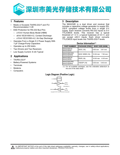
DOUTRIN250 kb/s IEC61000-4-2An IMPORTANT NOTICE at the end of this data sheet addresses availability,warranty,changes,use in safety-critical applications, intellectual property matters and other important disclaimers.PRODUCTION DATA.1Features•Meets or Exceeds TIA/RS-232-F and ITURecommendation V.28•ESD Protection for RS-232Bus Pins–±15-kV Human-Body Model(HBM)–±8-kV IEC61000-4-2,Contact Discharge–±15-kV IEC61000-4-2,Air-Gap Discharge•Operates From a Single5-V Power Supply With1-µF Charge-Pump Capacitors•Operates up to250kbit/s•Two Drivers and Two Receivers•Low Supply Current:8mA Typical2Applications•TIA/RS-232-F•Battery-Powered Systems•Terminals•Modems•Computers3DescriptionThe MAX232E is a dual driver and receiver thatincludes a capacitive voltage generator to supply RS-232-F compliant voltage levels from a single5-Vsupply.Each receiver converts RS-232inputs to5-VTTL/CMOS levels.This receiver has a typicalthreshold of1.3V,a typical hysteresis of0.5V,andcan accept±30-V inputs.Each driver convertsTTL/CMOS input levels into TIA/RS-232-F levels.Device Information(1)PART NUMBER PACKAGE(PINS)BODY SIZE(NOM)MAX232ECDMAX232EIDSOIC(16)9.90mm×3.91mmMAX232ECDWMAX232EIDWSOIC WIDE(16)10.30mm×7.50mmMAX232ECNMAX232EINPDIP(16)19.30mm×6.35mmMAX232ECPWMAX232EIPWTSSOP(16) 5.00mm×4.40mm(1)For all available packages,see the orderable addendum atthe end of the data sheet.Logic Diagram(Positive Logic)14MAX232ESLLS723C –APRIL 2006–REVISED AUGUST 2016Product Folder Links:MAX232E Submit Documentation FeedbackCopyright ©2006–2016,Texas Instruments Incorporated12Device and Documentation Support12.1Receiving Notification of Documentation UpdatesTo receive notification of documentation updates,navigate to the device product folder on .In the upper right corner,click on Alert me to register and receive a weekly digest of any product information that has changed.For change details,review the revision history included in any revised document.12.2Community ResourcesThe following links connect to TI community resources.Linked contents are provided "AS IS"by the respective contributors.They do not constitute TI specifications and do not necessarily reflect TI's views;see TI's Terms of Use .TI E2E™Online Community TI's Engineer-to-Engineer (E2E)Community.Created to foster collaborationamong engineers.At ,you can ask questions,share knowledge,explore ideas and helpsolve problems with fellow engineers.Design Support TI's Design Support Quickly find helpful E2E forums along with design support tools andcontact information for technical support.12.3TrademarksE2E is a trademark of Texas Instruments.All other trademarks are the property of their respective owners.12.4Electrostatic Discharge CautionThis integrated circuit can be damaged by ESD.Texas Instruments recommends that all integrated circuits be handled with appropriate precautions.Failure to observe proper handling and installation procedures can cause damage.ESD damage can range from subtle performance degradation to complete device failure.Precision integrated circuits may be more susceptible to damage because very small parametric changes could cause the device not to meet its published specifications.12.5GlossarySLYZ022—TI Glossary .This glossary lists and explains terms,acronyms,and definitions.13Mechanical,Packaging,and Orderable InformationThe following pages include mechanical,packaging,and orderable information.This information is the most current data available for the designated devices.This data is subject to change without notice and revision of this document.For browser-based versions of this data sheet,refer to the left-hand navigation.。
adi6832芯片手册

adi6832芯片手册ADI6832是一款功能强大的芯片,广泛应用于各种电子设备中。
本文将对ADI6832芯片进行详细介绍,包括其主要特性、应用领域、工作原理以及使用注意事项等内容。
ADI6832芯片是一款高性能的集成电路,由美国ADI公司设计并生产。
它采用了先进的技术和工艺,具有多种功能和特性,适用于各种应用场景。
首先,我们来了解ADI6832芯片的主要特性。
该芯片采用了8核心架构,每个核心都具有独立的处理能力,可以同时进行多任务处理。
此外,ADI6832芯片还具有高速缓存和高带宽内存接口,可以有效提高数据访问速度和处理效率。
其次,ADI6832芯片具有广泛的应用领域。
由于其高性能和多功能特性,该芯片可以广泛应用于各种电子设备中,例如智能手机、平板电脑、电视机、路由器等。
在这些设备中,ADI6832芯片可以实现高清视频播放、图像处理、数据加密等功能,为用户提供更好的使用体验。
接下来,我们来了解ADI6832芯片的工作原理。
该芯片采用了先进的指令集架构,通过多核心同时处理任务,提高了系统的响应速度和处理效率。
其内置的高速缓存和内存接口可以快速读取和写入数据,保证了数据处理的高效性。
然而,在使用ADI6832芯片时,也需要注意一些事项。
首先,需要正确连接芯片的电源和信号线,确保电路连接正常。
其次,使用过程中需要注意芯片的散热问题,避免芯片过热影响正常工作。
最后,芯片的引脚和功能需要正确配置和使用,避免不必要的错误和故障发生。
综上所述,ADI6832芯片是一款功能强大的集成电路,具有多种特性和应用领域。
在各种电子设备中,该芯片可以实现高性能的数据处理和功能实现,为用户提供更好的使用体验。
然而,在使用时,也需要遵循相应的使用要求和注意事项,以确保芯片的正常工作和可靠性。
相信随着技术的不断发展,ADI6832芯片将在未来的电子设备中发挥更大的作用,并为用户带来更多的便利和使用效果。
- 1、下载文档前请自行甄别文档内容的完整性,平台不提供额外的编辑、内容补充、找答案等附加服务。
- 2、"仅部分预览"的文档,不可在线预览部分如存在完整性等问题,可反馈申请退款(可完整预览的文档不适用该条件!)。
- 3、如文档侵犯您的权益,请联系客服反馈,我们会尽快为您处理(人工客服工作时间:9:00-18:30)。
General DescriptionThe MAX6832–MAX6840 are microprocessor (µP)supervisory circuits used to monitor low-voltage power supplies in µP and digital systems. They provide excel-lent circuit reliability and low cost by eliminating exter-nal components and adjustments when used with +1.2V to +1.8V powered circuits.These devices assert a reset signal whenever the V CC supply voltage declines below a preset threshold or whenever manual reset (MR ) is asserted. Reset remains asserted for a fixed timeout delay after V CC has risen above the reset threshold or when manual reset is deasserted. Five different timeout periods are available:70µs (voltage detector), 1.5ms, 30ms, 210ms, and 1.68s.Reset thresholds suitable for operation with a variety of supply voltages are available.The MAX6832/MAX6835/MAX6838 have a push-pull active-low reset output (RESET ). The MAX6833/MAX6836/MAX6839 have a push-pull active-high reset output (RESET) and the MAX6834/MAX6837/MAX6840have an open-drain active-low reset output (RESET ). The open-drain active-low reset output requires a pullup resis-tor that can be connected to a voltage higher than V CC . The MAX6835/MAX6836/MAX6837 feature a debounced manual reset input (MR ), while the MAX6838/MAX6839/MAX6840 provide a RESET-IN input allowing the user to externally adjust the reset threshold. The reset compara-tor is designed to ignore fast transients on V CC .Low supply current of 7.5µA makes the MAX6832–MAX6840 ideal for use in portable equipment. These devices are available in 3- and 4-pin SC70 packages.ApplicationsComputers ControllersIntelligent InstrumentsCritical µP and µC Power Monitoring Portable/Battery-Powered EquipmentFeatureso Factory-Set Reset Threshold Voltages for Nominal Supplies from 1.2V to 1.8V o Low Power Consumption: 7.5µA (typ) o Space-Saving 3- and 4-Pin SC70 Packages o ±2.5% Reset Threshold Accuracy Over Temperatureo Five Different Timeout Periods Available: 70µs (voltage detector), 1.5ms, 30ms, 210ms, and 1.68s o Three Reset Output ConfigurationsPush-Pull RESET Push-Pull RESET Open-Drain RESET o Guaranteed Reset Valid to V CC =0.55V—Active-Low 0.75V—Active-High o Adjustable Threshold Reset-In Option o Manual Reset Input Optiono Immune to Short Negative V CC Transients o Pin Compatible with MAX803/MAX809/MAX810,MAX6711/MAX6712/MAX6713, and MAX6381–MAX6390 SeriesMAX6832–MAX6840Ultra-Low-Voltage SC70 Voltage Detectorsand µP Reset Circuits________________________________________________________________Maxim Integrated Products 1Ordering Information19-2242; Rev 1; 1/02For pricing, delivery, and ordering information,please contact Maxim/Dallas Direct!at 1-888-629-4642, or visit Maxim’s website at .Pin Configurations appear at end of data sheet.Typical Operating Circuit apears at end of data sheet.Selector Guide appears at end of data sheet.Insert the desired suffix letter from the Threshold Suffix Guide (MAX6832–MAX6837) and the Active Timeout Period Guide tables into the blanks to complete the part number. Sample stock is generally available on standard versions only (seeStandard Versions table). Standard versions require a minimum order increment of 2.5k units. Nonstandard versions must be ordered in 10k unit increments. Contact factory for availability.All parts are offered in tape-and-reel only.M A X 6832–M A X 6840Ultra-Low-Voltage SC70 Voltage Detectors and µP Reset Circuits 2_______________________________________________________________________________________ABSOLUTE MAXIMUM RATINGSELECTRICAL CHARACTERISTICS(V CC = +0.55V to +3.6V, T A = T MIN to T MAX , unless otherwise noted. Typical values are at T A = +25°C.) (Note 1)Stresses beyond those listed under “Absolute Maximum Ratings” may cause permanent damage to the device. These are stress ratings only, and functional operation of the device at these or any other conditions beyond those indicated in the operational sections of the specifications is not implied. Exposure to absolute maximum rating conditions for extended periods may affect device reliability.Terminal Voltage (with respect to GND)V CC ........................................................................-0.3V to +6.0V Open-Drain RESET , MR .......................................-0.3V to +6.0V RESET-IN, Push-Pull RESETand RESET..............................................-0.3V to (V CC + 0.3V)Input/Output Current (all pins)............................................20mAContinous Power Dissipation (T A = +70°C)3-Pin SC70 (derate 2.9mW/°C above +70°C)...............235mW 4-Pin SC70 (derate 3.1mW/°C above +70°C)...............245mW Operating Temperature Range ...........................-40°C to +85°C Junction Temperature......................................................+150°C Storage Temperature Range.............................-65°C to +150°C Lead Temperature (soldering, 10s).................................+300°CMAX6832–MAX6840Ultra-Low-Voltage SC70 Voltage Detectorsand µP Reset Circuits_______________________________________________________________________________________3ELECTRICAL CHARACTERISTICS (continued)(V CC = +0.55V to +3.6V, T A = T MIN to T MAX , unless otherwise noted. Typical values are at T A = +25°C.) (Note 1)Note 2:Temperature range is from 0°C to +85°C.M A X 6832–M A X 6840Ultra-Low-Voltage SC70 Voltage Detectors and µP Reset Circuits 4_______________________________________________________________________________________Typical Operating Characteristics(V CC = full range and T A = -40°C to +85°C, unless otherwise noted. Typical values are at T A = +25°C).SUPPLY CURRENT vs. TEMPERATURE0264121410816S U P P L Y C U R R E N T (µA )-4020-20406080TEMPERATURE (°C)010050200150250300-402040-206080POWER-DOWN RESET DELAYvs. TEMPERATURETEMPERATURE (°C)P O W E R -D O W N R E S E TD E L A Y (µs )0.9940.9960.9950.9990.9980.9971.0021.0011.0001.003-400-2020406080NORMALIZED RESET THRESHOLDvs. TEMPERATURETEMPERATURE (°C)N O R M A L I Z ED RE S E T T H R E S H O L D0.940.980.961.021.001.041.06-402040-206080NORMALIZED POWER-UP RESET TIMEOUT vs. TEMPERATURETEMPERATURE (°C)N O R M A L I Z E D R E S E T T I M E O U T P E R I O DMAX6832–MAX6840Ultra-Low-Voltage SC70 Voltage Detectorsand µP Reset Circuits_______________________________________________________________________________________5M A X 6832–M A X 6840Detailed DescriptionReset OutputA microprocessor ’s (µP ’s) reset input starts the µP in a known state. The MAX6832–MAX6840 assert a reset to prevent code-execution errors during power-up, power-down, or brownout conditions. They also assert a reset signal whenever the V CC supply voltage falls below a preset threshold (MAX6832–MAX6837) or RESET-IN falls below the adjustable threshold (MAX6838/MAX6839/MAX6840), keeping reset asserted for a fixed timeout delay (Table 2) after V CC or RESET-IN has risen above the reset threshold. The MAX6832/MAX6835/MAX6838 use a push-pull active-low output, the MAX6833/MAX6836/MAX6839 have a push-pull active-high output, and the MAX6834/MAX6837/MAX6840have an open-drain active-low output stage. Connect a pullup resistor on the MAX6834/MAX6837/MAX6840’s RESET output to any supply between 0 and 6V.Manual Reset InputMany µP-based systems require manual reset capabili-ty, allowing the operator, a test technician, or external logic circuitry to initiate a reset. Reset remains asserted while MR is low, and for a fixed timeout delay after MR returns high. This input has an internal 20k Ωpullup resistor, so it can be left open if it is not used. MR can be driven with CMOS logic level, or with open-drain/col-lector outputs. To create a manual reset function, con-nect a normally open momentary switch from MR to ground; external debounce circuitry is not required. IfMR is driven from long cables or if the device is used in a noisy environment, connecting a 0.1µF capacitor from MR to ground provides additional noise immunity.RESET-IN InformationThe MAX6838/MAX6839/MAX6840 feature a RESET-IN input for monitoring supply voltages down to 0.44V. An external resistive-divider network can be used to set voltage monitoring thresholds as shown in Figure 1. As the monitored voltage falls, the voltage at RESET-IN decreases and asserts a reset when it falls below the RESET-IN threshold (V RSTIN ). The low-leakage currentUltra-Low-Voltage SC70 Voltage Detectors and µP Reset Circuits 6_______________________________________________________________________________________Functional DiagramsFigure 1. Setting the Adjustable Threshold Externallyat RESET-IN allows for relatively large-value resistors to be used, which reduce power consumption. For exam-ple, for a 0.6V monitored trip level, if R2 = 200k Ω, then R1 = 70.3k Ω. Note that the minimum V CC of 1.1V is required to guarantee the RESET-IN threshold accura-cy (see Electrical Characteristics table).Applications InformationNegative-Going V CC TransientsIn addition to issuing a reset to the µP during power-up,power-down, and brownout conditions, the MAX6832–MAX6840 are relatively immune to short-duration nega-tive-going V CC transients (glitches).Figure 2 shows typical transient duration vs. reset com-parator overdrive, for which the MAX6832–MAX6840 do not generate a reset pulse. The graph was generated using a negative-going pulse applied to V CC , starting 0.1V above the actual reset threshold and ending below it by the magnitude indicated (reset comparator overdrive). The graph indicates the maximum pulse width a negative-going V CC transient can have without causing a reset pulse. As the magnitude of the tran-sient increases (goes farther below the reset threshold),the maximum allowable pulse width decreases. A 0.1µF bypass capacitor mounted as close as possible to the V CC pin provides additional transient immunity.Ensuring a Valid Reset OutputDown to V CC = 0When V CC falls below 0.55V, the MAX6832/MAX6835/MAX6838 push-pull RESET output no longer sinks cur-rent —it becomes an open circuit. Therefore, high-impedance CMOS logic inputs connected to RESETcan drift to undetermined voltages. This presents no problem in most applications since most µP and other circuitry are inoperative with V CC lower than 0.55V.However, in applications where RESET must be valid down to 0, adding a pulldown resistor to RESET causes any stray leakage currents to flow to ground, holding RESET low (Figure 3). R3’s value is not critical; 100k Ωis large enough not to load RESET and small enough to pull RESET to ground.A 100k Ωpullup resistor to V CC is also recommended for the MAX6833/MAX6836/MAX6839 if RESET is required to remain valid for V CC < 0.85V.Interfacing to µPs with BidirectionalReset PinsSince the RESET output on the MAX6834/MAX6837/MAX6840 is open-drain, these devices interface easily with µPs that have bidirectional reset pins. Connecting the µP supervisor ’s RESET output directly to the µP ’s RESET pin with a single pullup resistor allows either device to assert a reset (Figure 4).MAX6832–MAX6840Ultra-Low-Voltage SC70 Voltage Detectorsand µP Reset Circuits_______________________________________________________________________________________7Figure 2. Maximum Transient Duration Without Causing a Reset Pulse vs. Reset Comparator OverdriveFigure 3. RESET Valid to V CC = Ground CircuitFigure 4. Interfacing to µPs with Bidirectional Reset I/OM A X 6832–M A X 6840Using The MAX6834/MAX6837/MAX6840Open-Drain RESET Outputwith Multiple SuppliesG enerally, the pullup connected to the MAX6834/MAX6837/MAX6840 will connect to the supply voltage that is being monitored at the IC ’s V CC pin. However,some systems may use the open-drain output to level-shift from the monitored supply to reset circuitry pow-ered by some other supply (Figure 5). Note that as the MAX6834/MAX6837/MAX6840’s V CC decreases, so does the IC ’s ability to sink current at RESET . Also, with any pullup, RESET will be pulled high as V CC declines toward 0. The voltage where this occurs depends on the pullup resistor value and the voltage to which it is connected.Chip InformationTRANSISTOR COUNT: 681PROCESS: BiCMOSUltra-Low-Voltage SC70 Voltage Detectors and µP Reset Circuits 8_______________________________________________________________________________________Figure 5. Using The MAX6834/MAX6837/MAX6840 Open-Drain RESETOutput with Multiple SuppliesTable 3. Standard VersionsTable 1. Threshold Suffix GuideSelector GuideMAX6832–MAX6840Ultra-Low-Voltage SC70 Voltage Detectorsand µP Reset Circuits_______________________________________________________________________________________9Typical Operating CircuitPin ConfigurationsTable 3. Standard Versions (continued)Selector Guide (continued)M A X 6832–M A X 6840Ultra-Low-Voltage SC70 Voltage Detectors and µP Reset Circuits 10______________________________________________________________________________________Package InformationMAX6832–MAX6840Ultra-Low-Voltage SC70 Voltage Detectors and µP Reset CircuitsMaxim cannot assume responsibility for use of any circuitry other than circuitry entirely embodied in a Maxim product. No circuit patent licenses are implied. Maxim reserves the right to change the circuitry and specifications without notice at any time.Maxim Integrated Products, 120 San Gabriel Drive, Sunnyvale, CA 94086 408-737-7600 ____________________11©2002 Maxim Integrated Products Printed USAis a registered trademark of Maxim Integrated Products.Package Information (continued)元器件交易网。