5.0SMLJ13A中文资料
MAA50-2K051512SBN中文资料

Single-output modelsModule МАА50- 1S03S ХХ МАА50- 1S05S ХХ МАА50- 1S12S ХХ МАА50- 1S15S ХХ МАА50- 1S24S ХХ МАА50- 1S27S ХХМАА50- 1S48S ХХ МАА50- 1S68S ХХ Output power 26,4 W 40 W 50 W Output voltage 3,3 VDC 5 VDC12 VDC15 VDC24 VDC27 VDC48 VDC68 VDCOutput current8 A8 А 4,17 А 3,33 А 2,27 А 1,85 А 1,04 А 0,73 АDual-output modelsModule МАА50-2S0505S ХХ МАА50-2S1212S ХХМАА50-2S1515S ХХOutput power 50 WChannel number 1 2 1 2 1 2 Output voltage 5 VDC 5 VDC 12 VDC 12 VDC15 VDC 15 VDC Output current5 А 5 А 2,1 А 2,1 А 1,67 А 1,67 АTriple-output modelsModule МАА50-3S051212S ХХМАА50-3S051515S ХХOutput power 50 WChannel number 1 2 3 1 2 3Output voltage 5 VDC12 VDC12 VDC5 VDC15 VDC15 VDCOutput current5 А 1,04А 1,04А 5 А 0,83 А 0,83 Аby request can be delivered modules with non-standard output voltage from 3 to 70 VDC and maximal output current to 8А.Ordering informationМАА 50 – 3 S 05 15 15 S U Nc d e f g h i j k lc - MAA Seriesd - Nominal output power, Watte - Channel quantity (1, 2, 3)f - - Input voltageS – 220VAC K – 115VACg - Output voltage channel 1, VDC h - Output voltage channel 2, VDC i - Output voltage channel 3, VDC j - Execution with sealing k - EmbodimentB – uniform case with primingl - Operating temperature range of caseN - - 40°С…+85°С P - - 50°С…+85°С• Rugged environment in operation intechnical equipment of industrial and special purpose. • Low-profile construction • Metal case• Cooling by heat sink or free air convection• Electromagnetic compatibility index to GOST V 25803-91 for group 1.2.1 (curve 2) • Stability to external factors of group 1U GOST RV 20.39.414.1-97 (additional) • Short circuit protection, overload, overvoltage and thermal protection • Galvanic isolated outputs •Acceptance «5»Температура окружающей среды Токр, С9080706050403020100-10-20-30-40-50Выходная мощность, Вт6050403020100Input specificationsParameter Conditions of dimensions MIN NOM MAX UnitS 187 220 242 VACSteady-state deviationК 80 115 140 VAC S 176 264 VACInput voltageTransient deflection, 1 secК 80 150 VAC SInput frequencyК47 400 440 HzOutput specificationsParameterConditions of dimensions MIN NOM MAX Unit Single-output execution (Inom 10 – 100%) ±3 % Output 1 multi-output execution(Inom 10 – 100%) ±3 %Uout2&3 differs from Uout1 less than 20% Output 2 and 3 multi-output execution(Inom 10 – 100%)±13 %Output 1 multi-output execution (Inom 30 – 100%) ±3 %Total output voltage instabilityUout2&3differs fromUout1 more than 20% Output 2 and 3 multi-output execution(Inom 50-100%) ±15 %Output voltage pulsations ripple(peak-to-peak)Dimension by device for pulsation control2% Uout.nom.Current overload protection actuation level110 % Iout.nom. Short circuit protection Autorepair 150 % Iout.nom. Overvoltage protection 120 % Uout.nom.Thermal protection90-95°CGeneral specificationsParameterConditions of dimensions MIN NOM MAX Unit- operating of case N P – 40 – 50 +85+85°C– power loss See diagram Temperature– storage – 50 +85 °CEfficiency 78 % Conversion frequency 50 kHz~ in/out 1500 VAC ~ in/case 1500 VAC~ out/case 500 VDC Isolation~ out/out 500 VDCInsulation resistance Voltage 500VDC 20 Ohm High humidity Temperature 35°С 98 % Cyclic overpatching of temperature – 60 +85 °C Multiple mechanical shocks Speeding-up 15g 2 15 ms Sinusoidal vibration Speeding-up 5g 50 500 Hz Atmosphere pressure 6х104 1,2х105 Pa Time to failure Temperature 35°C 105 hour Mass 0,4 kg all specifications redused for normal climatic conditions, Uin.nom., Iout.nom., if it is not specified differently.Power loss diagramFree airconvectionWith heat sinkAmbient temperature Tamb, °CO u t p u t p o w e r , WOutput settings№ pin1 2 3 4 5 6 7 8 9 Single-channel case ~IN (N) ~IN (L) +out1 +out1 +out1 -out1 -out1 -out1 Dual-channel case ~IN (N) ~IN (L) +out1 +out1 -out1 -out1 -out2 +out2 Triple-channelcase~IN (N)~IN (L)-out3+out3+out1-out1-out2+out2Switching on standart diagramFU in – current safety device 1A for input voltage 220VAC, 2A for input voltage 115VAC.S out – ceramic condenser capacity 0,47-15 mcF with corresponding operating voltage to decrease high-frequency noise level.S out2 – electronic condenser capacity 22-100 mcF in consideration with operating voltage and polarity. It makes for purpose to decrease dynamic instability when module work at dynamic load.+Out -Out ~In (L) ~In (N) Power module R heat CaseСout1 Сout2~In (L)~In (N)ground FU inSingle, Dual, and Triple-output execution SBNSingle, Dual, and Triple-output execution SVN (with flexible erection joints)The Flexible erection fjoints by length (100±5)mm is executed by wire section (0,5...1,5)mm2.。
标准倍速链铝型材型号

标准倍速链铝型材型号一、概述倍速链铝型材是一种高质量、高效率的输送链条,适用于各种自动化生产线和装配线。
其型号繁多,根据不同的需求和应用场景,可以选择合适的型号以满足生产要求。
本文将介绍标准倍速链铝型材的型号和特点,以及如何选择合适的型号。
二、倍速链铝型材型号1. 轻型倍速链铝型材轻型倍速链铝型材是较轻的输送链条,适用于轻量物品的输送。
其材质轻巧,结构简单,安装方便,成本较低。
常用的规格有1012、1515等。
2. 标准倍速链铝型材标准倍速链铝型材是应用最广泛的输送链条,适用于中量物品的输送。
其材质坚固,结构紧凑,运行稳定,维护方便。
常用的规格有1520、2025、2530等。
3. 重型倍速链铝型材重型倍速链铝型材适用于重型物品的输送,具有较高的承载能力和稳定性。
其材质厚实,结构坚固,运行平稳,适用于大规模生产线。
常用的规格有3040、4050等。
三、倍速链铝型材的特点1. 材质优良:倍速链铝型材采用高品质铝合金材料制作,具有优异的耐腐蚀性和耐磨性,能够保证长期稳定的使用。
2. 结构紧凑:倍速链铝型材采用紧凑的设计,能够有效地节省空间,降低安装难度。
同时,其结构简单,维护方便,降低了维护成本。
3. 运行稳定:倍速链铝型材采用精密的加工工艺,确保了链条的平稳运行。
其承载能力强,运行速度快,能够满足各种生产需求。
4. 易于调整:倍速链铝型材的长度可以根据需要进行调整,方便安装和拆卸。
同时,其链节间距可调,适用于不同长度的输送线。
四、如何选择合适的倍速链铝型材型号在选择合适的倍速链铝型材型号时,需要考虑以下因素:1. 输送物品的重量:根据输送物品的重量选择合适的型号,确保链条能够承受物品的重量并保持稳定运行。
2. 输送线的长度和高度:根据输送线的长度和高度选择合适的型号,以确保链条在输送过程中能够保持平稳并降低噪音。
3. 生产节拍和输送速度:选择能够满足生产节拍和输送速度要求的型号,以确保生产线的顺畅运行。
3680系列精密潜入杆电阻器产品说明书
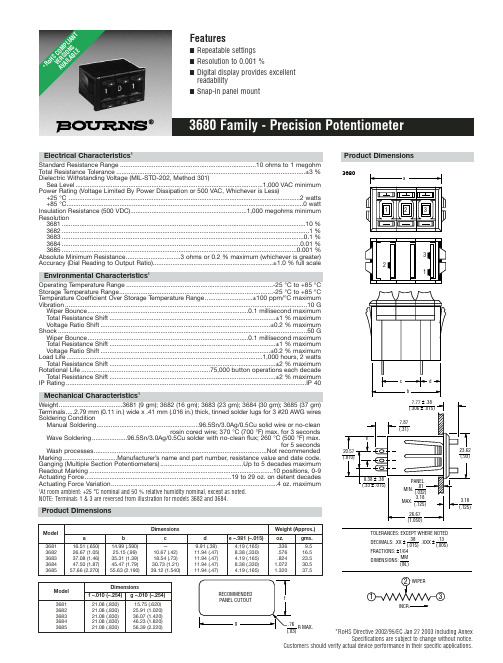
*RoHS Directive 2002/95/EC Jan 27 2003 including AnnexSpecifications are subject to change without notice.Customers should verify actual device performance in their specific applications.Electrical Characteristics 1Standard Resistance Range .............................................................................10 ohms to 1 megohm Total Resistance Tolerance...........................................................................................................±3 %Dielectric Withstanding Voltage (MIL-STD-202, Method 301)Sea Level..........................................................................................................1,000 VAC minimum Power Rating (Voltage Limited By Power Dissipation or 500 VAC, Whichever is Less)+25 °C ...................................................................................................................................2 watts +85 °C......................................................................................................................................0 watt Insulation Resistance (500 VDC)..................................................................1,000 megohms minimum Resolution3681..........................................................................................................................................10 %3682............................................................................................................................................1 %3683.........................................................................................................................................0.1 %3684.......................................................................................................................................0.01 %3685.....................................................................................................................................0.001 %Absolute Minimum Resistance...............................3 ohms or 0.2 % maximum (whichever is greater)Accuracy (Dial Reading to Output Ratio)....................................................................±1.0 % full scaleEnvironmental Characteristics1Operating Temperature Range ...................................................................................-25 °C to +85 °C Storage Temperature Range.......................................................................................-25 °C to +85 °C Temperature Coefficient Over Storage Temperature Range...........................±100 ppm/°C maximum Vibration.........................................................................................................................................10 G Wiper Bounce...........................................................................................0.1 millisecond maximum Total Resistance Shift..............................................................................................±1 % maximum Voltage Ratio Shift................................................................................................±0.2 % maximum Shock.............................................................................................................................................50 G Wiper Bounce...........................................................................................0.1 millisecond maximum Total Resistance Shift..............................................................................................±1 % maximum Voltage Ratio Shift................................................................................................±0.2 % maximum Load Life...............................................................................................................1,000 hours, 2 watts Total Resistance Shift..............................................................................................±2 % maximum Rotational Life.........................................................................75,000 button operations each decade Total Resistance Shift..............................................................................................±2 % maximum IP Rating........................................................................................................................................IP 40Mechanical Characteristics 1Weight....................................3681 (9 gm); 3682 (16 gm); 3683 (23 gm); 3684 (30 gm); 3685 (37 gm)T erminals.....2.79 mm (0.11 in.) wide x .41 mm (.016 in.) thick, tinned solder lugs for 3 #20 AWG wires Soldering ConditionManual Soldering..........................................................96.5Sn/3.0Ag/0.5Cu solid wire or no-cleanrosin cored wire; 370 °C (700 °F) max. for 3 secondsWave Soldering....................96.5Sn/3.0Ag/0.5Cu solder with no-clean flux; 260 °C (500 °F) max.for 5 secondsWash processes..................................................................................................Not recommended Marking...............................Manufacturer’s name and part number, resistance value and date code.Ganging (Multiple Section Potentiometers)...............................................Up to 5 decades maximum Readout Marking........................................................................................................10 positions, 0-9Actuating Force...................................................................................19 to 29 oz. on detent decades Actuating Force Variation..............................................................................................4 oz. maximum1At room ambient: +25 °C nominal and 50 % relative humidity nominal, except as noted.NOTE: Terminals 1 & 3 are reversed from illustration for models 3682 and 3684.3680INCR.Product DimensionsDimensionsWeight (Approx.)Model a b c d e –.381 (–.015)oz.gms.368116.51 (.650)14.99 (.590)—9.91 (.39) 4.19 (.165).3369.5368226.67 (1.05)25.15 (.99)10.67 (.42)11.94 (.47)8.38 (.330).57616.5368337.08 (1.46)35.31 (1.39)18.54 (.73)11.94 (.47) 4.19 (.165).82423.5368447.50 (1.87)45.47 (1.79)30.73 (1.21)11.94 (.47)8.38 (.330) 1.07230.5368557.66 (2.270)55.63 (2.190)39.12 (1.540)11.94 (.47)4.19 (.165)1.32037.5DimensionsModel f –.010 (–.254)g –.010 (–.254)368121.08 (.830)15.75 (.620)368221.08 (.830)25.91 (1.020)368321.08 (.830)36.07 (1.420)368421.08 (.830)46.23 (1.820)368521.08 (.830)56.39 (2.220)*Ro H S C O M P L I A N T V E R S I O N S A V A I L A B L ESpecifications are subject to change without notice.Customers should verify actual device performance in their specific applications.Recommended Part NumbersBOLDFACE LISTINGS ARE IN STOCK AND READILY AVAILABLE THROUGH DISTRIBUTION.FOR OTHER OPTIONS CONSULT FACTORY.RoHS IDENTIFIER:L =COMPLIANTBLANK =NON-COMPLIANTREV. 05/07。
BUS13A中文资料

1 4 0.8
µS
Semelab Plc reserves the right to change test conditions, parameter limits and package dimensions without notice. Information furnished by Semelab is believed to be both accurate and reliable at the time of going to press. However Semelab assumes no responsibility for any errors or omissions discovered in its use. Semelab encourages customers to verify that datasheets are current before placing orders.
VCESM VCEO IC ICM IB IBM Ptot Tstg TJ RθJ-MB Collector – Emitter Voltage (VBE = 0, peak value) Collector – Emitter Voltage (Open Base) Collector Current Collector Current (Peak Value)tp<2ms Base Current (d.c.) Base Current (Peak Value) tp<2ms Total Power Dissipation up to Tmb = 25°C Storage Temperature Junction Temperature Thermal Resistance (junction-mounting base) 1000V 450V 15A 30A 6A 9A 175W –65 to +200°C 200°C 1.0°C/W
常用的稀土镁合金种类
常用的稀土镁合金种类
稀土镁合金是一种高性能的轻质合金,由稀土元素和镁元素组成。
它具有优异的力学性能、耐腐蚀性能和耐高温性能,广泛应用于航空、汽车、电子、医疗等领域。
下面介绍几种常用的稀土镁合金种类。
1. AZ91D合金
AZ91D合金是一种常用的稀土镁合金,由9%铝和1%锌组成,加入稀土元素后,可以提高合金的强度和耐腐蚀性能。
该合金具有优异的机械性能和加工性能,广泛应用于汽车、航空、电子等领域。
2. AM50A合金
AM50A合金是一种含铝的稀土镁合金,由5%铝和0.5%锰组成,加入稀土元素后,可以提高合金的强度和耐腐蚀性能。
该合金具有优异的机械性能和加工性能,广泛应用于汽车、航空、电子等领域。
3. WE43合金
WE43合金是一种高强度的稀土镁合金,由4%铝、3%锆和0.5%稀土元素组成,具有优异的机械性能和耐腐蚀性能。
该合金广泛应用于航空、航天、国防等领域,是一种重要的结构材料。
4. ZK60A合金
ZK60A合金是一种含锆的稀土镁合金,由5.5%锌、0.45%锆和0.8%稀土元素组成,具有优异的机械性能和耐腐蚀性能。
该合金广泛应用于航空、汽车、电子等领域,是一种重要的结构材料。
稀土镁合金是一种重要的轻质合金,具有优异的机械性能、耐腐蚀性能和耐高温性能,广泛应用于航空、汽车、电子、医疗等领域。
不同种类的稀土镁合金具有不同的组成和性能,可以根据具体的应用需求选择合适的合金。
SMAJ5.0A-TR中文资料

SMAJ5.0A-TR,CA-TR SMAJ188A-TR,CA-TRTRANSIL TM®PEAK PULSE POWER : 400 W (10/1000µs)STAND OFF VOLTAGE RANGE :From 5V to 188V.UNI AND BIDIRECTIONAL TYPES LOW CLAMPING FACTOR FAST RESPONSE TIMEJEDEC REGISTERED PACKAGE OUTLINE FEATURESSMA(JEDEC D0214 AC)Symbol ParameterValue Unit P PP Peak pulse power dissipation (see note 1)Tj initial = T amb 400W P Power dissipation on infinite heatsink T amb = 50°C 3.3W I FSM Non repetitive surge peak forward current for unidirectional types tp = 10msTj initial = T amb40A T stg T j Storage temperature range Maximum junction temperature- 65 to + 175150°C °C T LMaximum lead temperature for soldering during 10 s.260°CNote 1 : For a surge greater than the maximum values, the diode will fail in short-circuit.ABSOLUTE MAXIMUM RATINGS (T amb = 25°C)DESCRIPTIONThe SMAJ series are TRANSIL TM diodes designed specifically for protecting sensitive equipment against transient overvoltages. The SMA package allows save spacing on high density printed circuit boards.Transil diodes provide high overvoltage protection by clamping action. Their instantaneous response to transient overvoltages makes them particularly suited to protect voltage sensitive devices such as MOS Technology and low voltage supplied IC’s.September 1998 Ed: 5A Symbol ParameterValue Unit R th (j-l)Junction to leads30°C/W R th (j-a)Junction to ambient on printed circuit on recommended pad layout120°C/WTHERMAL RESISTANCES 1/5II F V F V CLV BRV RMI PPI RMVSymbol ParameterV RM Stand-off voltage V BR Breakdown voltage V CL Clamping voltage I RM Leakage current @ V RM I PPPeak pulse currentαTVoltage temperature coefficient V FForward voltage dropELECTRICAL CHARACTERISTICS (T amb = 25°C)TypesI RM @ V RM V BR @ I R V CL @ I PP V CL @ I PP αT C maxmin maxmaxmaxtyp note210/1000µs 8/20µs note3note4Unidirectional Mark.Bidirectional Mark. µA V V mA V A V A 10-4/°C pF SMAJ5.0A-TR AE SMAJ5.0CA-TR AA 800 5.0 6.4109.243.513.4174 5.73500SMAJ6.0A-TR DUB SMAJ6.0CA-TR DBB 800 6.0 6.71010.338.813.7170 5.93300SMAJ6.5A-TR DUC SMAJ6.5CA-TR DBC 500 6.57.21011.235.714.5160 6.13100SMAJ8.5A-TR DUH SMAJ8.5CA-TR DBH 108.59.44114.427.718.61247.32000SMAJ10A-TR AX SMAJ10CA-TR AC 51011.111723.521.71067.81550SMAJ12A-TR DUK SMAJ12CA-TR DBK 51213.3119.920.125.3918.31325SMAJ13A-TR BG SMAJ13CA-TR BH 11314.4121.518.627.2858.41200SMAJ15A-TR BM SMAJ15CA-TR AJ 11516.7124.416.432.5718.8975SMAJ18A-TR DUQ SMAJ18CA-TR DBQ 11820129.213.739.3599.2800SMAJ20A-TR DUR SMAJ20CA-TR DBR 12022.2132.412.342.8549.4725SMAJ22A-TR DUS SMAJ22CA-TR DBS 12224.4135.511.248.3489.6625SMAJ24A-TR DUT SMAJ24CA-TR DBT 12426.7138.910.350469.6600SMAJ26A-TR DUU SMAJ26CA-TR DBU 12628.9142.19.553.5439.7575SMAJ28A-TR CG SMAJ28CA-TR CH 12831.1145.48.859399.8510SMAJ30A-TR CK SMAJ30CA-TR CL 13033.3148.48.364.3369.9480SMAJ33A-TR CM SMAJ33CA-TR CN 13336.7153.37.569.73310.0450SMAJ40A-TR DUZ SMAJ40CA-TR DBZ 14044.4164.5 6.2842710.1370SMAJ43A-TR EUA SMAJ43CA-TR EBA 14347.8169.4 5.7912510.2350SMAJ48A-TR CX SMAJ48CA-TR CY 14853.3177.4 5.21002310.3320SMAJ58A-TR EUF SMAJ58CA-TR EBF 15864.4193.6 4.31211910.4270SMAJ70A-TR EUI SMAJ70CA-TR EBI 17077.81113 3.51461610.5230SMAJ85A-TR EUL SMAJ85CA-TR EBL 18594.41137 2.91781310.6200SMAJ100A-TR EUN SMAJ100CA-TR EBN 11001111162 2.52121110.7170SMAJ130A-TR EUQ SMAJ130CA-TR EBQ 11301441209 1.9265910.8145SMAJ154A-TR EUT SMAJ154CA-TR EBT 11541711246 1.6317710.8125SMAJ170A-TR SR SMAJ170CA-TR SS 11701891275 1.4353 6.510.8120SMAJ188A-TREUV SMAJ188CA-TR EBV 11882091328 1.4388610.8110Note 2 :Pulse test : t p < 50 ms.Note 3 :∆V BR = αT * (T amb - 25) * V BR (25°C).Note 4 :V R = 0 V, F = 1 MHz. For bidirectional types,capacitance value is divided by 2.10s1000s%I PP 50tPULSE WAVEFORM 10/1000s100SMAJxxxA-TR, CA-TR2/52550751001251501750.00.10.20.30.40.50.60.70.80.91.01.1Ppp[Tj initial]/Ppp[Tj initial=25°C]Tj initial(°C)Fig 1: Peak power dissipation versus initial junction temperature.0.010.101.0010.0010010005000Ppp(W)tp(ms)Fig 2: Peak pulse power versus exponential pulse duration (Tj initial=25°C).1101005000.11.010.0100.0200.0Ipp(A)tp=20µstp=1ms SMAJ5.0A,CASMAJ188A,CASMAJ58A,CASMAJ26A,CASMAJ13A,CAV (V)CL Fig 3: Clamping voltage versus peak pulse current (Tj initial=25°C)Exponential waveform tp=20µs & tp=1ms.1101002001010010005000C(pF)F=1MHzSMAJ5.0ASMAJ188ASMAJ58ASMAJ26A SMAJ13A V (V)R Fig 4-1: Capacitance versus reverse applied voltage (typical values) (SMAJxxA).11010020011010010002000F=1MHzSMAJ5.0CA SMAJ188CASMAJ58CA SMAJ26CA SMAJ13CAC(pF)V (V)R Fig 4-2: Capacitance versus reverse applied voltage (typical values) (SMAJxxCA).SMAJxxxA-TR, CA-TR3/50.40.50.60.70.80.9 1.0 1.1 1.2 1.3 1.40.010.101.0010.00I (A)FM Tj=25°CTj=125°CV (V)FM Fig 5: Peak forward voltage drop versus peak forward current (typical values).1E-21E-11E+01E+11E+25E+20.010.101.00Zth(j-a)/Rth(j-a)tp(s)Fig 6: Relative variation of thermal impedance junction to ambient versus pulse duration.12345405060708090100110120130140Rth(j-a) (°C/W)S(Cu)(cm²)Fig 7: Thermal resistance junction to ambient versus copper surface under each lead (printed circuit board FR4 e(Cu)=35µm).2550751001251501E-11E+01E+11E+21E+32E+3I [Tj] / I [Tj=25°C]R R V < 8.5VBR Tj(°C)V 8.5VBR ≥Fig 8: Relative variation of leakage current versus junction temperature.SMAJxxxA-TR, CA-TR4/5REF.DIMENSIONSMillimeters Inches Min.Max.Min.Max.A11.902.700.0750.106A20.050.200.0020.008b1.25 1.650.0490.065c 0.150.410.0060.016E4.805.600.1890.220E13.954.600.1560.181D 2.25 2.950.0890.116L0.751.600.0300.063Information furnished is believed to be accurate and reliable. However, STMicroelectronics assumes no responsibility for the consequences of use of such information nor for any infringement of patents or other rights of third parties which may result from its use. No license is granted by implication or otherwise under any patent or patent rights of STMicroelectronics.Specifications mentioned in this publication are subject to change without notice. This publication supersedes and replaces all information previously supplied.STMicroelectronics products are not authorized for use as critical components in life support devices or systems without express written approval of STMicroelectronics.The ST logo is a registered trademark of STMicroelectronics © 1998 STMicroelectronics - Printed in Italy - All rights reserved.STMicroelectronics GROUP OF COMPANIESAustralia - Brazil - Canada - China - France - Germany - Italy - Japan - Korea - Malaysia - Malta - Mexico - Morocco -The Netherlands - Singapore - Spain - Sweden - Switzerland - Taiwan - Thailand - United Kingdom - U.S.A.Packaging : standard packaging is in tape and reel.PACKAGE MECHANICAL DATA SMA (Plastic)ECLE1DA1A2bMARKING : Logo, Date Code, Type Code, Cathode Band (for unidirectional types only).FOOTPRINT DIMENSIONS (Millimeter)SMA Plastic.2.40 1.651.45 1.45Weight = 0.068 gORDER CODESM A J 85 C A - TRBIDIRECTIONALNo suffix : UnidirectionalSURFACE MOUNTSTAND OFF VOLTAGE400 WATTSTAPE & REEL SMAJxxxA-TR, CA-TR5/5。
LJA系列 安全用限位开关 说明书

→安全用LJS -A LJS -PA LJHLJS -ELJS -TELJA 系列安全用限位开关内置快动机构、附带接点强制开离机构,适应一般工业机械的EC机器指示说明及取得CE标志所必不可少的安全限位开关。
●带 标志(带正反馈电路操作的控制开关的符号),已取得EN规格认证。
● 符合EN50041规格。
● 带UL/CSA/CE/CCC标志,最适用于向北美、欧洲、中国出口的机械。
● 通过快动机构实现常闭/常开的电气独立接点(Zb)。
● 提高接触可靠性的双接点结构。
● 应用广泛的LS通用型限位开关、适宜的安装间距。
● 丰富多样的触动头种类。
● 防浸型(JIS)、IP67(IEC 60529)的高封密性。
■型号一览表UL/CSA/CE/CCC照片所示为滚轮连杆型。
详细尺寸请在图纸中确认。
常开固定接点1常开固定接点1常开固定接点2常开可动接点板1常开可动接点板1常开固定接点常开可动接点板常开可动接点板2柱塞柱塞绝缘块绝缘块常闭可动接点板2常闭可动接点板常闭固定接点2常闭固定接点接点强制开离凸轮可动接点翻转弹簧负载负载负载负载负载熔结熔结绝 缘 体绝 缘 体顶上通过快动使接点翻转安全用LJS -A LJS -PALJHLJS-ELJS -TE■内部开关:常闭/常开电气独立接点(Zb)LJA 的内部开关具有常闭/常开电气独立接点(Zb),且为双接点结构。
常闭接点用可动接点板和常开接点用可动接点板各自独立、相互绝缘,且具有双接点的二电路双断开关。
■LJA内部开关动作的说明●以往的LS通用型限位开关……●LJA……在以往的二电路双断开关中,当常闭接点熔结的情况下开关发生动作时,常闭和常开之间可能会呈导通状态。
此时,在某些电路结构中,可能会发生电源短路、负载烧毁等现象。
在LJA 系列中,即使在接点熔结的情况下开关发生动作,常闭和常开之间也不会导通。
因此,如上图所示,即使在常闭侧和常开侧连接不同的电源,也能避免电源短路、负载烧毁等现象的发生。
SMBJ13A中文资料
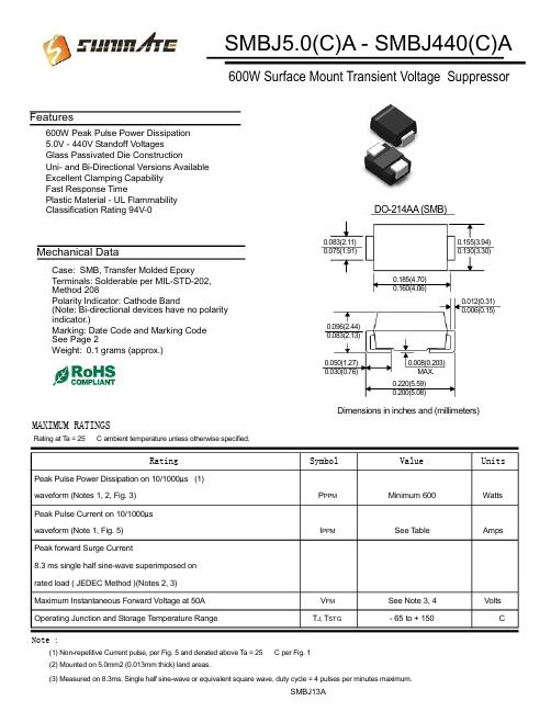
SMBJ5.0(C)A - SMBJ440(C)A600W Surface Mount Transient Voltage SuppressorFeatures600W Peak Pulse Power Dissipation5.0V - 440V Standoff VoltagesGlass Passivated Die ConstructionUni- and Bi-Directional Versions AvailableExcellent Clamping CapabilityFast Response TimePlastic Material - UL FlammabilityClassification Rating 94V-0Mechanical DataCase: SMB, Transfer Molded EpoxyTerminals: Solderable per MIL-STD-202,Method 208Polarity Indicator: Cathode Band(Note: Bi-directional devices have no polarityindicator.)Marking: Date Code and Marking CodeSee Page 2Weight: 0.1 grams (approx.)MAXIMUM RATINGSRating at T a = 25 C ambient temperature unless otherwise specified.DO-214AA (SMB)0.083(2.11) 0.155(3.94) 0.075(1.91) 0.130(3.30)0.185(4.70)0.160(4.06)0.012(0.31)0.006(0.15) 0.096(2.44)0.083(2.13)0.050(1.27) 0.008(0.203)0.030(0.76) MAX.0.220(5.59)0.200(5.08)Dimensions in inches and (millimeters)Rating Symbol Value Units Peak Pulse Power Dissipation on 10/1000μs (1)waveform (Notes 1, 2, Fig. 3) P PPM Minimum 600 Watts Peak Pulse Current on 10/1000μswaveform (Note 1, Fig. 5) I PPM See T able Amps Peak forward Surge Current8.3 ms single half sine-wave superimposed onrated load ( JEDEC Method )(Notes 2, 3)Maximum Instantaneous Forward Voltage at 50A V FM See Note 3, 4 Volts Operating Junction and Storage T emperature Range T J, T STG - 65 to + 150 CNote :(1) Non-repetitive Current pulse, per Fig. 5 and derated above Ta = 25 C per Fig. 1(2) Mounted on 5.0mm2 (0.013mm thick) land areas.(3) Measured on 8.3ms. Single half sine-wave or equivalent square wave, duty cycle = 4 pulses per minutes maximum.SMBJ13ATYPE MarkingReverse BreakdownStand-Off VoltageVoltage Min. @I TBreakdownVoltage TestMax. @ I T CurrentMaximumClampingVoltage@I PPPeak ReversePulse LeakageCurrent @V RMW(Uni) (BI) (Uni) (Bi) V RMW (V) V BR MIN(V) V BR MAX(V) I T (mA) V C(V) I PP(A) I R(uA) SMBJ5.0 SMBJ5.0C KD AD 5.0 6.40 7.55 10 9.6 62.5 800.0 SMBJ5.0A SMBJ5.0CA KE AE 5.0 6.40 7.25 10 9.2 65.2 800.0 SMBJ6.0 SMBJ6.0C KF AF 6.0 6.67 8.45 10 11.4 52.6 800.0 SMBJ6.0A SMBJ6.0CA KG AG 6.0 6.67 7.67 10 10.3 58.3 800.0 SMBJ6.5 SMBJ6.5C KH AH 6.5 7.22 9.14 10 12.3 48.8 500.0 SMBJ6.5A SMBJ6.5CA KK AK 6.5 7.22 8.30 10 11.2 53.6 500.0 SMBJ7.0 SMBJ7.0C KL AL 7.0 7.78 9.86 10 13.3 45.1 200.0 SMBJ7.0A SMBJ7.0CA KM AM 7.0 7.78 8.95 10 12.0 50.0 200.0 SMBJ7.5 SMBJ7.5C KN AN 7.5 8.33 10.67 1.0 14.3 42.0 100.0 SMBJ7.5A SMBJ7.5CA KP AP 7.5 8.33 9.58 1.0 12.9 46.5 100.0 SMBJ8.0 SMBJ8.0C KQ AQ 8.0 8.89 11.3 1.0 15.0 40.0 50.0 SMBJ8.0A SMBJ8.0CA KR AR 8.0 8.89 10.23 1.0 13.6 44.1 50.0 SMBJ8.5 SMBJ8.5C KS AS 8.5 9.44 11.92 1.0 15.9 37.7 20.0 SMBJ8.5A SMBJ8.5CA KT AT 8.5 9.44 10.82 1.0 14.4 41.7 20.0 SMBJ9.0 SMBJ9.0C KU AU 9.0 10.0 12.6 1.0 16.9 35.5 10.0 SMBJ9.0A SMBJ9.0CA KV AV 9.0 10.0 11.5 1.0 15.4 39.0 10.0 SMBJ10 SMBJ10C KW AW 10 11.1 14.1 1.0 18.8 31.9 5.0 SMBJ10A SMBJ10CA KX AX 10 11.1 12.8 1.0 17.0 35.3 5.0 SMBJ11 SMBJ11C KY AY 11 12.2 15.4 1.0 20.1 29.9 5.0 SMBJ11A SMBJ11CA KZ AZ 11 12.2 14.0 1.0 18.2 33.0 5.0 SMBJ12 SMBJ12C LD BD 12 13.3 16.9 1.0 22.0 27.3 5.0 SMBJ12A SMBJ12CA LE BE 12 13.3 15.3 1.0 19.9 30.2 5.0 SMBJ13 SMBJ13C LF BF 13 14.4 18.2 1.0 23.8 25.2 5.0 SMBJ13A SMBJ13CA LG BG 13 14.4 16.5 1.0 21.5 27.9 5.0 SMBJ14 SMBJ14C LH BH 14 15.6 19.8 1.0 25.8 23.3 5.0 SMBJ14A SMBJ14CA LK BK 14 15.6 17.9 1.0 23.2 25.9 5.0 SMBJ15 SMBJ15C LL BL 15 16.7 21.1 1.0 26.9 22.3 5.0 SMBJ15A SMBJ15CA LM BM 15 16.7 19.2 1.0 24.4 24.6 5.0 SMBJ16 SMBJ16C LN BN 16 17.8 22.6 1.0 28.8 20.8 5.0 SMBJ16A SMBJ16CA LP BP 16 17.8 20.5 1.0 26.0 23.1 5.0 SMBJ17 SMBJ17C LQ BQ 17 18.9 23.9 1.0 30.5 19.7 5.0 SMBJ17A SMBJ17CA LR BR 17 18.9 21.7 1.0 27.6 21.7 5.0 SMBJ18 SMBJ18C LS BS 18 20.0 25.3 1.0 32.2 18.6 5.0 SMBJ18A SMBJ18CA LT BT 18 20.0 23.3 1.0 29.2 20.5 5.0 SMBJ20 SMBJ20C LU BU 20 22.2 28.1 1.0 35.8 16.8 5.0 SMBJ20A SMBJ20CA LV BV 20 22.2 25.5 1.0 32.4 18.5 5.0 SMBJ22 SMBJ22C LW BW 22 24.4 30.9 1.0 39.4 15.2 5.0 SMBJ22A SMBJ22CA LX BX 22 24.4 28.0 1.0 35.5 16.9 5.0 SMBJ24 SMBJ24C LY BY 24 26.7 33.8 1.0 43.0 14.0 5.0 SMBJ24A SMBJ24CA LZ BZ 24 26.7 30.7 1.0 38.9 15.4 5.0 SMBJ26 SMBJ26C MD CD 26 28.9 36.6 1.0 46.6 12.9 5.0 SMBJ26A SMBJ26CA ME CE 26 28.9 33.2 1.0 42.1 14.3 5.0 SMBJ28 SMBJ28C MF CF 28 31.1 39.4 1.0 50.0 12.0 5.0 SMBJ28A SMBJ28CA MG CG 28 31.1 35.8 1.0 45.4 13.2 5.0 Note:( 1 ) V BR measured after I T applied for 300 s., I T = square wave pulse or equivalent. ( 2 )Surge Current Waveform per Figure 5 and Derate per Figure 1( 3 ) A Transient suppressor is normally selected according to the reverse " Stand-off Voltage " (V WM) which should beequal to or greater then the D.C. or continuous peak operating voltage level.SMBJ13AReverse Breakdown Breakdown Maximum Peak Reverse TYPE Marking Stand-Off Voltage Voltage Test Clamping Pulse LeakageVoltage Min. @I T Max. @ I T Current Voltage @I PP Current @V RMW (Uni) (BI) (Uni) (Bi) V RMW (V) V BR MIN(V) V BR MAX(V) I T (mA) V C(V) I PP(A) I R(uA) SMBJ30 SMBJ30C MH CH 30 33.3 42.2 1.0 53.5 11.2 5.0 SMBJ30A SMBJ30CA MK CK 30 33.3 38.3 1.0 48.4 12.4 5.0 SMBJ33 SMBJ33C ML CL 33 36.7 46.5 1.0 59.0 10.2 5.0 SMBJ33A SMBJ33CA MM CM 33 36.7 42.2 1.0 53.3 11.3 5.0 SMBJ36 SMBJ36C MN CN 36 40.0 50.7 1.0 64.3 9.3 5.0 SMBJ36A SMBJ36CA MP CP 36 40.0 46.0 1.0 58.1 10.3 5.0 SMBJ40 SMBJ40C MQ CQ 40 44.4 56.3 1.0 71.4 8.4 5.0 SMBJ40A SMBJ40CA MR CR 40 44.4 51.1 1.0 64.5 9.3 5.0 SMBJ43A SMBJ43CA MT CT 43 47.8 54.9 1.0 69.4 8.6 5.0 SMBJ45 SMBJ45C MU CU 45 50.0 63.3 1.0 80.3 7.5 5.0 SMBJ45A SMBJ45CA MV CV 45 50.0 57.5 1.0 72.7 8.3 5.0 SMBJ48 SMBJ48C MW CW 48 53.3 67.5 1.0 85.5 7.0 5.0 SMBJ48A SMBJ48CA MX CX 48 53.3 61.3 1.0 77.4 7.8 5.0 SMBJ51 SMBJ51C MY CY 51 56.7 71.8 1.0 91.1 6.6 5.0 SMBJ51A SMBJ51CA MZ CZ 51 56.7 65.2 1.0 82.4 7.3 5.0 SMBJ54 SMBJ54C ND DD 54 60.0 76.0 1.0 96.3 6.2 5.0 SMBJ54A SMBJ54CA NE DE 54 60.0 69.0 1.0 87.1 6.9 5.0 SMBJ58 SMBJ58C NF DF 58 64.4 81.6 1.0 103 5.8 5.0 SMBJ58A SMBJ58CA NG DG 58 64.4 74.1 1.0 93.6 6.4 5.0 SMBJ60 SMBJ60C NH DH 60 66.7 84.5 1.0 107 5.6 5.0 SMBJ60A SMBJ60CA NK DK 60 66.7 76.7 1.0 96.8 6.2 5.0 SMBJ64 SMBJ64C NL DL 64 71.1 90.1 1.0 114 5.3 5.0 SMBJ64A SMBJ64CA NM DM 64 71.1 81.8 1.0 103 5.8 5.0 SMBJ70 SMBJ70C NN DN 70 77.8 98.6 1.0 125 4.8 5.0 SMBJ70A SMBJ70CA NP DP 70 77.8 89.5 1.0 113 5.3 5.0 SMBJ75 SMBJ75C NQ DQ 75 83.0 105.7 1.0 134 4.5 5.0 SMBJ75A SMBJ75CA NR DR 75 83.0 95.8 1.0 121 5.0 5.0 SMBJ90 SMBJ90C NW DW 90 100 126.5 1.0 160 3.8 5.0 SMBJ90A SMBJ90CA NX DX 90 100 115.5 1.0 146 4.1 5.0 SMBJ100 SMBJ100C NY DY 100 111 141.0 1.0 179 3.4 5.0 SMBJ100A SMBJ100CA NZ DZ 100 111 128.0 1.0 162 3.7 5.0 SMBJ110 SMBJ110C PD ED 110 122 154.5 1.0 196 3.1 5.0 SMBJ110A SMBJ110CA PE EE 100 122 140.5 1.0 177 3.4 5.0 SMBJ120 SMBJ120C PF EF 120 133 169.0 1.0 214 2.8 5.0 SMBJ120A SMBJ120CA PG EG 120 133 153.0 1.0 193 3.1 5.0 SMBJ130 SMBJ130C PH EH 130 144 182.5 1.0 231 2.6 5.0 SMBJ130A SMBJ130CA PK EK 130 144 165.5 1.0 209 2.9 5.0 SMBJ150 SMBJ150C PL EL 150 167 211.5 1.0 268 2.2 5.0 SMBJ150A SMBJ150CA PM EM 150 167 192.5 1.0 243 2.5 5.0 SMBJ160 SMBJ160C PN EN 160 178 226.0 1.0 287 2.1 5.0 SMBJ160A SMBJ160CA PP EP 160 178 205.0 1.0 259 2.3 5.0 Note:( 1 ) V BR measured after I T applied for 300 s., I T = square wave pulse or equivalent. ( 2 )Surge Current Waveform per Figure 5 and Derate per Figure 1( 3 ) A Transient suppressor is normally selected according to the reverse " Stand-off Voltage " (V WM) which should beequal to or greater then the D.C. or continuous peak operating voltage level.SMBJ13ATYPE MarkingReverse BreakdownStand-Off VoltageVoltage Min. @I TBreakdownVoltage TestMax. @ I T CurrentMaximumClampingVoltage@I PPPeak ReversePulse LeakageCurrent @V RMW(Uni) (BI) (Uni) (Bi) V RMW (V) V BR MIN(V) V BR MAX(V) I T (mA) V C(V) I PP(A) I R(uA) SMBJ170 SMBJ170C PQ EQ 170 189 239.5 1.0 304 2.0 5.0 SMBJ170A SMBJ170CA PR ER 170 189 217.5 1.0 275 2.2 5.0 SMBJ180 SMBJ180C PS ES 180 200 253.8 1.0 321 1.9 5.0 SMBJ180A SMBJ180CA PT ET 180 200 230.4 1.0 290 2.1 5.0 SMBJ190 SMBJ190C PU EU 190 211 267.9 1.0 339 1.8 5.0 SMBJ190A SMBJ190CA PV EV 190 211 243.2 1.0 306 2.0 5.0 SMBJ200 SMBJ200C PW EW 200 222 282.0 1.0 356 1.7 5.0 SMBJ200A SMBJ200CA PX EX 200 222 256.0 1.0 322 1.9 5.0 SMBJ210 SMBJ210C PY EY 210 233 296.1 1.0 375 1.6 5.0 SMBJ210A SMBJ210CA PZ EZ 210 233 268.8 1.0 339 1.8 5.0 SMBJ220 SMBJ220C QD FD 220 244 310.2 1.0 392 1.5 5.0 SMBJ220A SMBJ220CA QE FE 220 244 281.6 1.0 355 1.7 5.0 SMBJ250 SMBJ250C QF FF 250 278 342.5 1.0 447 1.3 5.0 SMBJ250A SMBJ250CA QG FG 250 278 309.0 1.0 403 1.5 5.0 SMBJ300 SMBJ300C QH FH 300 333 411.0 1.0 535 1.1 5.0 SMBJ300A SMBJ300CA QK FK 300 333 371.0 1.0 484 1.2 5.0 SMBJ350 SMBJ350C QL FL 350 389 479.5 1.0 624 1.0 5.0 SMBJ350A SMBJ350CA QM FM 350 389 432.0 1.0 565 1.1 5.0 SMBJ400 SMBJ400C QN FN 400 444 548.0 1.0 687 0.9 5.0 SMBJ400A SMBJ400CA QP FP 400 444 494.0 1.0 645 0.9 5.0 SMBJ440 SMBJ440C QQ FQ 440 489 602.8 1.0 786 0.8 5.0 SMBJ440A SMBJ440CA QR FR 440 489 543.0 1.0 710 0.8 5.0SMBJ13ARatings and Characteristic Curves T A =25癈 unless otherwise notedSMBJ13A。
- 1、下载文档前请自行甄别文档内容的完整性,平台不提供额外的编辑、内容补充、找答案等附加服务。
- 2、"仅部分预览"的文档,不可在线预览部分如存在完整性等问题,可反馈申请退款(可完整预览的文档不适用该条件!)。
- 3、如文档侵犯您的权益,请联系客服反馈,我们会尽快为您处理(人工客服工作时间:9:00-18:30)。
FeaturesMechanical DataTerminals: solderable per MIL-STD-750, Method 2026 Polarity: Color band denotes positive end( cathode) exceptBi-directional types.Standard packaging: 16mm tape per ( EIA 481). Weight: 0.007 ounce, 0.21 gramMaximum Ratings @ 25o C Unless Otherwise SpecifiedPeak Pulse Current on 10/1000uswaveform(Note1, Fig3)I PPM See Table 1Amps Peak Pulse Power Disspation on 10/1000us waveform(Note1,2,Fig1)P PPMMinimum 5000Watts Peak forward surge current (JEDEC Method) (Note 2,3)I FSM)300.0Amps Operation And Storage Temperature Range T J ,T STG -55o C to +150o CNOTES:1.Non-repetitive current pulse per Fig.3 and derated above TA=25oC per Fig.2.2.Mounted on 8.0mm 2copper pads to each terminal.3.8.3ms, single half sine-wave or equivalent square wave, duty cycle=4 pulses per. Minutes maximum.For surface mount application in order to optimize board space Low inductance Low profile package Built-in strain relief Glass passivated junction Excellent clamping capability Repetition Rate( duty cycle): 0.01%Fast response time: typical less than 1ps from 0V to BV min Typical I D less than 1uA above 10VHigh temperature soldering: 250oC/10 seconds at terminals Plastic package has Underwrites Laboratory FlammabilityClassification 94V-Oomp onents 20736 Marilla Street Chatsworth! "# $ % ! "#Revision: 1 2006/10/18 UL Recognized File # E222849TMMicro Commercial ComponentsCase Material: Molded Plastic. UL Flammability Classification Rating 94V-0www.mccsemi .com1 of 4MAXIMUM CLAMPING VOLTAGE REVERSE LEAKAGE @Ipp @V RWM Vc(V)I D (µA)5.0SMLJ 11A 1112.213.51018.22758005PEN 5.0SMLJ 12A 1213.314.71019.92528005PEP 5.0SMLJ 13A 1314.415.91021.52335005PEQ 5.0SMLJ 14A 1415.617.21023.22162005PER 5.0SMLJ 15A 1516.718.5124.42051005PES 5.0SMLJ 16A 1617.819.7126193505PET 5.0SMLJ 17A 1718.920.9127.6181205PEU 5.0SMLJ 18A 182022.1129.2172105PEV 5.0SMLJ 20A 2022.224.5132.415555PEW 5.0SMLJ 22A 2224.426.9135.514155PEX 5.0SMLJ 24A 2426.729.5138.912955PEZ 5.0SMLJ 26A 2628.931.9142.111955PFE 5.0SMLJ 28A 2831.134.4145.411055PFG 5.0SMLJ 30A 3033.336.8148.410355PFK 5.0SMLJ 33A 3336.740.6153.393.955PFM 5.0SMLJ 36A 364044.2158.186.155PFP 5.0SMLJ 40A 4044.449.1164.577.655PFR 5.0SMLJ 43A 4347.852.8169.472.155PFT 5.0SMLJ 45A 455055.3172.768.855PFV 5.0SMLJ 48A 4853.358.9177.464.755PFX 5.0SMLJ 51A 5156.762.7182.460.755PFZ 5.0SMLJ 54A 546066.3187.157.555RGE 5.0SMLJ 58A 5864.471.2193.653.555PGG 5.0SMLJ 60A 6066.773.7196.851.755PGK 5.0SMLJ 64A 6471.178.6110348.655PGM 5.0SMLJ 70A 7077.886111344.355PGP 5.0SMLJ 75A 7583.392.1112141.455PGR 5.0SMLJ 78A 7886.795.8112639.755PGT 5.0SMLJ 85A 8594.4104113736.555PGV 5.0SMLJ 90A 90100111114634.355PGX 5.0SMLJ 100A 100111123116230.955PGZ 5.0SMLJ 110A 110122135117728.355PHE 5.0SMLJ 120A 12013314711932655PHG 5.0SMLJ 130A 13014415912092455PHK 5.0SMLJ 150A 150167185124320.655PHM 5.0SMLJ 160A 160178197125919.355PHP 5.0SMLJ 170A170189209127518.255PHRDEVICE MARKING CODE PART NUMBERPEAK PULSE CURRENT Ipp (A)TEST CURRENT I T (mA)BREAKDOWNVOLTAGE V BR (V)MAX.@ITBREAKDOWN VOLTAGEV BR (V)MIN.@IT REVERSE STAND- OFF VOLTAGE V RWM (V)TMMicro Commercial Components5.0SMLJ11A~5.0SMLJ170Awww.mccsemi .com2 of 4Revision: 1 2006/10/18MAXIMUM CLAMPING VOLTAGE REVERSE LEAKAGE @Ipp @V RWM Vc(V)I D (µA)5.0SMLJ 11CA 1112.213.51018.22758005BEN 5.0SMLJ 12CA 1213.314.71019.92528005BEP 5.0SMLJ 13CA 1314.415.91021.52335005BEQ 5.0SMLJ 14CA 1415.617.21023.22162005BER 5.0SMLJ 15CA 1516.718.5124.42051005BES 5.0SMLJ 16CA 1617.819.7126193505BET 5.0SMLJ 17CA 1718.920.9127.6181205BEU 5.0SMLJ 18CA 182022.1129.2172105BEV 5.0SMLJ 20CA 2022.224.5132.415555BEW 5.0SMLJ 22CA 2224.426.9135.514155BEX 5.0SMLJ 24CA 2426.729.5138.912955BEZ 5.0SMLJ 26CA 2628.931.9142.111955BFE 5.0SMLJ 28CA 2831.134.4145.411055BFG 5.0SMLJ 30CA 3033.336.8148.410355BFK 5.0SMLJ 33CA 3336.740.6153.393.955BFM 5.0SMLJ 36CA 364044.2158.186.155BFP 5.0SMLJ 40CA 4044.449.1164.577.655BFR 5.0SMLJ 43CA 4347.852.8169.472.155BFT 5.0SMLJ 45CA455055.3172.768.855BFVPART NUMBERREVERSE STAND- OFF VOLTAGE V RWM (V)BREAKDOWN VOLTAGEV BR (V)MIN.@IT BREAKDOWNVOLTAGE V BR (V)MAX.@ITTEST CURRENT I T (mA)PEAK PULSE CURRENT Ipp (A)DEVICE MARKING CODE TMMicro Commercial Components5.0SMLJ11C A~5.0SMLJ 45C AFor Bidirectional type having Vrwm of 20 volts and less,the Ir limit is double.www.mccsemi .com3 of 4Revision: 1 2006/10/18Revision: 12006/10/18Micro Commercial Componentswww.mccsemi .com4 of 4products are represented on our website, harmless against all damages.***APPLICATIONS DISCLAIMER******IMPORTANT NOTICE***Aerospace or Military Applications.Products offer by Micro Commercial Components Corp .are not intended for use in Medical,Micro Commercial Components Corp .reserve s the right to make changes without further notice to any product herein to make corrections, modifications , enhancements , improvements , or other changes .Micro Commercial Components Corp .does not assume any liability arising out of the application or use of any product described herein; neither does it convey any license under its patent rights ,nor the rights of others . The user of products in such applications shall assume all risks of such use and will agree to hold Micro Commercial Components Corp .and all the companies whose。