MAX3010EUP中文资料
串口max30100工作原理
串口max30100工作原理
串口Max30100是一种集成了红外发光二极管、光电二极管和数
字信号处理器的模块,用于心率和血氧饱和度测量。
其工作原理如下:
1. 发光二极管发射红外光和可见光,Max30100模块中的发光
二极管会发射红外光和可见光到皮肤表面。
2. 光电二极管接收反射光,光电二极管接收到皮肤表面反射回
来的红外光和可见光。
3. 数字信号处理器处理光电二极管接收到的光信号,Max30100
模块中的数字信号处理器会对光电二极管接收到的光信号进行处理,提取出血液脉搏的信号。
4. 通过串口输出数据,处理后的血氧饱和度和心率数据通过串
口输出,可以通过串口连接到微处理器或者计算机进行进一步的处
理和分析。
总的来说,串口Max30100模块通过发射光并接收反射光,利用
数字信号处理器对光信号进行处理,最终通过串口输出血氧饱和度和心率数据。
这种工作原理使得Max30100模块在医疗监护、运动健康等领域有着广泛的应用。
基于MAX30100传感器心率检测实现的作品报告解答

_______ 学年度实践学期学生实践报告年月日一年月日项目名称: ____________________________ 指导教师: ____________________________ 课题: _______________________________系另比____________________________ 专业班级: ____________________________ 学号: _______________________________ 学生姓名: ____________________________本学期的小学期实践设计项目作品,为基于单片机MCI开发箱的心率传感器开发,该主体采用IAP15W4K58S4型号MCU单片机作为本项目的开发系统,以及基于MAX30100芯片的传感器。
电源供配采用MCI开发箱自带的恒压电源,数据显示采用由两片HC595动态驱动的8 个数码管。
考虑到对本项目作品的使用与数据采样处理,本人采用最高具有16 位精度的MAX30100芯片传感器作为主要的心率数据采集模块,MAX30100芯片内部集成ADC数据转换,以及多个可读写寄存器,本作品主要操作其中的FIFO寄存器进行数据采集。
同时MAX30100芯片传感器属于I2C 接口器件,故在程序开发中,采用I2C 接口协议进行。
关键词:单片机MCI开发箱;MAX3O1O0传感器;HC595 FIFO寄存器;I2C ;免责申明:本报告为本人作为学生所作报告,报告中个别部分(图片、伪代码、芯片介绍等)存在局部摘取他人成果,本人已做出作品后现发出本报告纯为分享学习,不做他途,故请大家善取善用。
1一、 ......................................................................... 项目目的31.1、项目目的 (3)1.2、项目目标 (3)二、 ............................................................... 项目内容及硬件设计42.1、系统器件介绍 (4)2.2、各电路模块 (4)三、 ......................................................................... 软件设计53.1、程序开发使用软件 (5)3.2、程序流程图 (5)3.3、代码示例(ma in函数部分) (6)3.4、算法问题及分析 (8)3.4.1、关于整体代码框架中存在的问题 (8)3.4.2、关于对MAX30100芯片的硬件驱动 (8)3.4.3、关于在驱动FIFO时需要注意的细节 (9)3.4.4、关于对项目硬件调试 (9)四、 ....................................................................... 总结与展望102五、 ............................................................................. 附录11作品图片.................................................................... 11 一、项目目的及目标1.1 、项目目的:随着人类的科技文明发展的进步,人们越发开始关注人们自身生活的质量及健康安全,而随可穿戴设备及物联网的发展,心率统计也从此开始全面进入人们的视野及生活。
迈普路由器产品手册【word版】2p
目录一、迈普路由器产品系列 ..........................................................................................1MP8800系列万兆核心路由器 ...........................................................................2MP7500全冗余ATCA核心路由器...................................................................3MP3800系列开放式全业务汇聚路由器 ...........................................................4MP2900系列开放式高速接入路由器 ...............................................................5MP2824系列开放式全业务接入路由器 ...........................................................6MP2800系列增强型宽窄带一体化智能路由器 ...............................................7MP1800系列3G专业级路由器 ........................................................................8MP1800-20 3G无线路由器 ................................................................................9MP IMR800 3G无线路由器 ...............................................................................二、迈普交换机产品系列 ..........................................................................................1MyPower S11800系列数据中心级核心交换机 ................................................2MyPower S8900系列高性能电信级交换机 ......................................................3MyPower S6800系列万兆核心路由交换机 ......................................................4MyPower S6600系列万兆汇聚路由交换机 ......................................................5MyPower S5800系列数据中心级接入交换机 ..................................................6MyPower S4320系列增强型千兆汇聚路由交换机 ..........................................7MyPower S4300系列增强型千兆汇聚路由交换机 ..........................................8MyPower S4220系列全千兆汇聚路由交换机 ..................................................9MyPower S4200系列千兆汇聚路由交换机 ......................................................10MyPower S4100系列电信级智能三层交换机 ...........................................11MyPower S4000系列千兆汇聚路由交换机 ...............................................12MyPower S3320系列千兆智能型网管交换机 ...........................................13MyPower S3300系列千兆智能网管型交换机 ...........................................14MyPower S3220系列千兆智能网管型交换机 ...........................................15MyPower S3200系列千兆智能网管型交换机 ...........................................16MyPower S3120系列百兆智能网管型交换机 ...........................................17MyPower S3100系列千兆智能网管型交换机 ...........................................18MyPower S2000系列网管型交换机 ...........................................................三、迈普安全产品系列 ..............................................................................................1MPSec MSG4000-X1安全网关..........................................................................2MPSec MSG4000-G6安全网关..........................................................................3MPSec MSG4000-G4安全网关..........................................................................4MPSec MSG4000-G2安全网关..........................................................................5MPSec MSG4000-G1安全网关..........................................................................6MPSec MSG4000-F6安全网关 ..........................................................................7MPSec VPN3000系列VPN网关.......................................................................8电子政务外网IPSec VPN网关..........................................................................9MPSec ISG1000系列网关 ..................................................................................四、迈普应用与服务产品系列 ..................................................................................1Maipu Mico一体化信息安防系统 .....................................................................2终端信息安全管理系统 ......................................................................................3MPSec CMS证书管理服务器 ............................................................................4Maipu AAS迈普接入认证服务器......................................................................5Maipu Portal服务器 ............................................................................................6迈普智能3G综合业务管理平台 .......................................................................7MS8000系列智能传媒服务器 ...........................................................................8MT1000系列媒体网关 .......................................................................................9迈普网络自动化运维系统 ..................................................................................10Maipu Masterplan迈普统一网络管理平台.................................................11Maipu DeviceMaster迈普路由交换设备管理系统 ....................................12迈普管理支撑系统 .......................................................................................五、迈普无线网络产品系列 ......................................................................................1Masterplan迈普无线有线一体化网管软件 .......................................................2MyPower WA2000 11n系列智能AP .................................................................3MyPower WA2000 同频系列无线智能AP .......................................................4MyPower WNC6000智能无线控制器 ...............................................................5MyPower WNC6000同频智能无线控制器 .......................................................6MyPower WA1000 11n系列WLAN CPE终端 .................................................六、迈普统一通信产品系列 ......................................................................................1MyPower VG 6000系列媒体网关......................................................................2MyPower VG 2000系列媒体网关......................................................................3MyPower VG2000-x系列媒体网关 ...................................................................4MyPower VG 800系列媒体网关........................................................................5MyPower VG A600系列媒体网关.....................................................................6MyPower VEP600系列IP可视电话 .................................................................7MyPower VEP310系列IP话机 .........................................................................8MyPower VEP300系列IP话机 .........................................................................9MyPower UCA个人通信助手............................................................................10MyPower VC8100 IP通信服务器 ...............................................................11MyPower IP电话会议系统..........................................................................12MyPower VC8200协同视频服务器............................................................13MyPower MCC融信呼 ................................................................................14迈普MyPower ICR 录音软件.....................................................................。
MCM310使用说明R2

第1页 共8页MCM310多功能智能电力分析仪使用手册1、显示界面MCM310多功能智能电力分析仪,具有一个高清晰液晶显示屏,通过4个多功能键来切换测量显示界面以及进行编程设置。
(1)三相显示数据提示符 (2)相序提示符 (3)三相显示数据单位 (4)三相数据显示区域第2页 共8页(5)运行指示符 (6)定值设置提示符 (7)开关量输出状态提示符 (8)开关量输入状态提示符 (9)通讯提示符 (10)操作按钮2、按键说明:退出返回到上一级菜单,设定时可左移动光标 :显示测量值时可作为向上选择,设定时对数值进行减1操作: 显示测量值时可作为向下选择,设定时对数值进行加1操作ENTER :进入设置模式;设置相关参数后进行确认3、接线端子示意图4、端子意义说明端子号 符号 说明 建议用线截面积(平方毫米)1 UN 中性线 <42 IC- C相电流输出 <43 IC+ C相电流输入 <44 UC C相电压 <45 IB- B相电流输出 <46 IB+ B相电流输入 <47 UB B相电压 <48 IA- A相电流输出 <49 IA+ A相电流输入 <410 UA A相电压 <411 A1 通信口1RS-485+ <412 B1 通信口1RS-485- <413 S 通讯屏蔽地 <414 A2 通信口2RS-485+ <415 B2 通信口2RS-485- <416 AO1 4—20mA模拟量输出1(可选) <2.5(单芯线)17 AO- 4—20mA模拟量公共地(可选) <2.5(单芯线)18 AO2 4—20mA模拟量输出2(可选) <2.5(单芯线)19 NC20 L 电源输入L+ <421 NC22 N 电源输入N- <423 NC24 FG 接大地 <425 V- 备用电源24V负 <426 V+ 备用电源24V正 <4第3页共8页第4页 共8页27 R22 继电器2或者脉冲2输出(可选) <2.5(单芯线) 28 R21 继电器2或者脉冲2输出(可选) <2.5(单芯线) 29 R12 继电器1或者脉冲1输出(可选) <2.5(单芯线) 30 R11 继电器1或者脉冲1输出(可选)<2.5(单芯线) 31D4- D4开关量输入(光耦隔离) <1.5(单芯线) 32 D4+ D4开关量输入(光耦隔离) <1.5(单芯线) 33 D3- D3开关量输入(光耦隔离) <1.5(单芯线) 34 D3+ D3开关量输入(光耦隔离) <1.5(单芯线) 35 D2- D2开关量输入(光耦隔离) <1.5(单芯线) 36 D2+ D2开关量输入(光耦隔离) <1.5(单芯线) 37 D1- D1开关量输入(光耦隔离) <1.5(单芯线) 38D1+D1开关量输入(光耦隔离)<1.5(单芯线)5、接线方式5.1 电压电流测量部分○1测量电压小于375V (相)/650V (线), ○2测量电压大于375V (相)/650V (线), 三相四线系统,无PT,3CT ,接线方式 三相三线系统,有PT,3CT,接线方式 FUNC设置为0;并正确设置好CT变比、 FUNC设置为1;并正确设置好CT变比、 PT变比为1。
MAX15301数据手册中文版

MAX15301是一个全功能,高效,数字化的点负载(POL)操纵器与先进的电源治理和遥测功能与PID 为基础的数字电源稳压器,MAX15301采纳Maxim拥有专利的Intune的™自动补偿,状态空间操纵算法。
Intune 的操纵律是有效的小信号和大信号响应,占占空比饱和度的阻碍。
这排除需要用户以确信和设置的阈值从线性转换到非线性模式。
这些能力在快速环路的瞬态响应,并减少输出电容器的数量相较,竞争的模拟和数字操纵器。
MAX15301包括多种功能,以优化效率。
内部开关BabyBuck的稳压器可产生栅极驱动器和内部偏置电源,低功耗的操纵器。
一种先进的,高效率的MOSFET的栅极驱动器,具有自适应非重叠按时,而持续调整的高侧和低侧的按时和驱动电压的全范围内的电压,电流和温度,以尽可能减少开关损耗。
MAX15301设计最终客户的设计环境的初衷。
上的PMBus™兼容的串行总线接口进行通信的监控器监控和故障治理。
全套的电源治理功能,无需复杂和昂贵的测序和监控IC。
大体的DC-DC转换操作,可设置通过引脚搭接,并非需要用户配置固件。
这使得电源子系统的快速进展前完成板级系统的工程。
Maxim提供支持的硬件和软件配置MAX15301 ,MAX15301可在32引线,5mm×5mm TQFN封装,工作在-40°C至+85°C的温度范围内。
特点:的自动补偿功能能够确保稳固,同时优化瞬态性能2.在快速瞬态响应减少输出电容的非线性补偿结果3.差分远端电压传感许诺±1%V OUT精度在整个温度范围内(-40°C至+85°C)接口用于配置,操纵和监测5.支持电压定位6.提高效率(自适应非重叠时序驱动器)至14V的宽输入电压范围8.高效片上BabyBuck稳压器的自偏置9.输出电压范围从到10.进入预偏置输出启动11.可配置的软启动和软停止时刻12.固定工作频率同步(300kHz至1MHz)13.灵活的排序和故障治理14.引脚手动跳线配置(输出电压,从机地址,开关频率,电流限制)15.能够快速原型图表典型工作电路引脚名字功能1SYNC外部开关频率同步输入端。
迈普交换机产品介绍资料

迈普以太网交换机产品系列迈普以以太网交换机产品系列目录MyPower S6800 系列万兆核心路由交换机 (1)MyPower S4196E机架式汇聚路由交换机 (6)MyPower S4200 系列千兆汇聚路由交换机 (9)MyPower S4100 系列千兆汇聚路由交换机 (12)MyPower S3100 系列智能网管型汇聚交换机 (16)MyPower S3000 系列智能网管型汇聚交换机 (19)MP5100 系列网管型接入交换机 (22)MP5008B非网管型接入交换机 (25)典型应用 (27)典型应用一:企业办公局域网解决方案 (27)典型应用二:运营商宽带接入网络解决方案 (27)版权所有©2007 迈普(四川)通信技术有限公司,保留所有权利。
MyPower S6800 系列万兆核心路由交换机MyPower S6800 系列万兆核心路由交换机是迈普公司推出的新一代多业务高端核心交换机,它采用 ASIC+NP 的体系结构设计,面向下一代网络提供稳定、可靠、安全的高性能 L2/L3 层交换服务,拥有 先进的万兆以太网支持,在保持线速转发性能的基础上,支持各种高密度接口板,满足核心层设备高密 度、高吞吐量的要求。
MyPower S6800 系列万兆核心路由交换机主要面向以业务为核心的企业网络架构 中新一代高端核心骨干交换设备,分别提供 4 槽、6 槽、10 槽、14 槽四种机框,分别提供 Gbps 级的背 板带宽和交换容量、Tbps 级的背板带宽和 Gbps 级的交换容量以及 Tbps 级的背板带宽和交换容量。
MyPower S6800 系列万兆核心路由交换机支持无源背板,支持主控冗余、电源冗余以及板卡、风扇、 电源热插拔多种电信级可靠性手段,并可以支持 STP/RSTP/MSTP/VRRP 等协议实现链路冗余,保障业 务的永续性。
MyPower S6800 系列万兆核心路由交换机支持丰富的 IPv6 实现技术,包括基于 NP 的集 中式硬件 IPv6 转发方式,以及基于 AISC 的分布式全线速硬件 IPv6 转发方式,能够满足不同规模的 IPv6 应用。
戴尔Chromebox会议室3010快速入门指南说明书
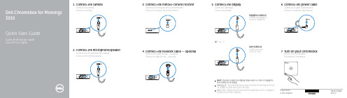
30101Connect the cameraConnecter la caméraConecte la cámara2Connect the microphone/speakerConnecter le microphone/haut-parleurConecte el micrófono/altavoz3Connect the remote-control receiverConnecter le récepteur de la télécommandeConecte el receptor de control remoto4Connect the network cable — optionalConnecter le câble réseau — facultatifConecte el cable de red — opcional5Connect the displayConnecter l’affichageConecte la pantallaDisplayPort connectorConnecteur DisplayPortConector DisplayPortOr | Ou | OHDMI connectorConnecteur HDMIConector HDMI6Connect the power cableConnecter le câble d’alimentationConecte el cable de alimentación7Turn on your ChromeboxActiver votre ChromeboxEncienda su Chromebox© 2014 Dell Inc.© 2014 Google Inc.Printed in Poland.2014-07NOTE:You have to switch the display’s input source to HDMI or DisplayPortafter turning on the display.REMARQUE : Vous devez basculer la source d’entrée de l’affichage vers HDMIou DisplayPort après avoir activé l’affichage.NOTA: debe cambiar la fuente de entrada de la pantalla a HDMI o DisplayPortdespués de encender la pantalla.FeaturesCaractéristiques | Características1. Power cable connector2. Network connector3. USB 3.0 connectors4. HDMI connector5. DisplayPort connector6. Headset connector7. USB 3.0 connectors withPowerShare 8. Power button/Power light 9. Memory-card reader10. Recovery buttonhole 11. Security cable slot 12. Microphone/Speaker 13. HD Camera14. Remote control - front 15. Keyboard-Remote control back1. Connecteur de câble d’alimentation2. Connecteur réseau3. Connecteurs USB 3.04. Connecteur HDMI5. Connecteur DisplayPort6. Connecteur de casque7. Connecteurs USB 3.0 avecPowerShare 8. Bouton d’alimentation/Voyant d’alimentation9. Lecteur de carte mémoire 10. Boutonnière de restauration 11. Emplacement pour câblede sécurité12. Microphone/Haut-parleur 13. Caméra HD14. Télécommande - avant 15. Clavier-Télécommande arrière1. Conector del cable de alimentación2. Conector de red3. Conectores USB 3.04. Conector HDMI5. Conector DisplayPort6. Conector de auriculares7. Conectores USB 3.0 conPowerShare 8. Botón de alimentación/Luz de alimentación9. Lector de tarjeta de memoria 10. Agujero de recuperación 11. Ranura para cable de seguridad 12. Micrófono/Altavoz 13. Cámara HD14. Control remoto - parte delantera 15. Teclado - control remoto partetraseraHelp CenterCentre d’aide | Centro de ayuda/chromeboxformeetings Contact DellContacter Dell | Póngase en contacto con Dell/contactdell /supportRegulatory and safetyRéglementation et sécurité | Reglamentación y seguridad /regulatory_compliance Regulatory modelModèle réglementaire | Modelo reglamentario Z01V Regulatory typeType réglementaire | Tipo reglamentario Z01V001Computer modelModèle d’ordinateur | Modelo de equipoDell Chromebox For Meetings 3010Información para NOM, o Norma Oficial MexicanaLa información que se proporciona a continuación se mostrará en los dispositivos que se describen en este documento, en conformidad con los requisitos de la Norma Oficial Mexicana (NOM):Importador:Dell México S.A. de C.V.Paseo de la Reforma 2620 - Piso 11.° Col. Lomas Altas 11950 México, D.F.Número de modelo reglamentario:Z01V, D09U Voltaje de entrada:19,5 VDC Corriente de entrada (máxima):3,34 A8Finish Chromebox setupTerminer la configuration de Chromebox | Finalice la configuración de ChromeboxYour Chromebox is now visible inAdmin ConsoleVotre Chromebox est maintenant visible dans la Console AdminPuede ver ahora su Chromebox en la Consola de administraciónVideo, audio, and microphone will be testedLa vidéo, l’audio et le microphone seront testésEl vídeo, audio y microfono serán probadosSign in to your Google accountConnectez-vous à votre compte Google Inicie sesión en su cuenta de GoogleVerify your network Vérifiez votre réseauCompruebe la red。
2019年MG3010便携式三相相位伏安表使用说明书

S使用说明书尊敬的顾客感谢您选用本公司的S MG3010便携式三相相位伏安表。
在您初次使用本仪器时,请先详细地阅读本说明书。
公司地址:武汉市东湖开发区光谷大道62号光谷总部国际4栋8楼销售热线:售后服务:传真网址一、简介该仪器以高性能的单片机作为中央处理器,采用三个独立的电压通道,三个独立的电流通道,三个电流钳,大屏幕图形点阵式液晶显示器,长效镍氢电池,电池管理电路,非易失性存储器,高精度时钟,串行数据接口的硬件设计,达到了便携式相位测量和多功能仪表的新高度,是传统双钳相位表所无法比拟的。
二、仪器用途本产品是理想的便携式相位测量及多功能仪器,具备以下功能:1、可以同时测量多至三路交流电压;2、可以在不断开被测电路的情况下(通过钳形电流互感器),同时测量多至三路交流电流;3、测量电压间、电流间、电压与电流间的相位差;4、测量频率;5、测量功率和功率因数;6、测量三相相序;7、测量零序电流。
由于仪器具有上述基本功能,其用途极为广泛:1、感性和容性电路的判别;2、继电保护各组CT之间相位关系;3、检查变压器接线组别;4、检查有功电度表接线正确与否;5、判断电度表运行快慢,合理收缴电费6、作为漏电流表使用等。
因此,该仪器是电力系统继电保护和计量专业、工矿企业、石油化工、冶金企业进行二次回路检查的理想仪表。
三、仪器特点1、一台仪器拥有七大功能:三相电压表、三相钳型电流表、相位表、相序表、频率计、功率表、功率因数表集于一身。
2、时测量(多至三相)电参数,并显示向量六角图。
3、钳形小电流准确测量,可作为泄漏电流表使用。
4、大屏幕点阵液晶,友好的人机界面。
5、长效镍氢电池,交直流两用电源,方便现场使用。
6、串行数据接口,可连接微型打印机及与计算机通讯7、屏幕(数据、图形)功能,方便查阅。
8、自换量程,软件校准。
9、高精度时钟,电池容量条形模拟显示。
10、全数字化,高可靠性。
四、技术指标1、测量范围1) 相位:0°~360°2) 电压:5~500V3) 电流:10mA~10A4) 频率:45~65Hz5) 功率因数:-1~+16) 功率:0~2、基本误差注:电流小于20mA时,相位误差小于±3°。
- 1、下载文档前请自行甄别文档内容的完整性,平台不提供额外的编辑、内容补充、找答案等附加服务。
- 2、"仅部分预览"的文档,不可在线预览部分如存在完整性等问题,可反馈申请退款(可完整预览的文档不适用该条件!)。
- 3、如文档侵犯您的权益,请联系客服反馈,我们会尽快为您处理(人工客服工作时间:9:00-18:30)。
General DescriptionThe MAX3000E/MAX3001E/MAX3002–MAX3012 8-channel level translators provide the level shifting nec-essary to allow data transfer in a multivoltage system.Externally applied voltages, V CC and V L , set the logic lev-els on either side of the device. Logic signals present on the V L side of the device appear as a higher voltage logic signal on the V CC side of the device, and vice-versa.The MAX3000E/MAX3001E/MAX3002/MAX3003 use an architecture specifically designed to be bidirectional without the use of a directional pin.The MAX3000E/MAX3001E/MAX3002/MAX3004–MAX3012feature an EN input that, when low, reduces the V CC and V L supply currents to < 2µA. The MAX3000E/MAX3001E also have ±15kV ESD protection on the I/O V CC side for greater protection in applications that route signals externally. The MAX3000E operates at a guaranteed data rate of 230kbps. The MAX3001E operates at a guaranteed data rate of 4Mbps. The MAX3002–MAX3012 operate at a guaranteed data rate of 20Mbps over the entire specified operating voltage range.The MAX3000E/MAX3001E/MAX3002–MAX3012 accept V L voltages from +1.2V to +5.5V and V CC voltages from +1.65V to +5.5V, making them ideal for data transfer between low-voltage ASICs/PLDs and higher voltage systems. The MAX3000E/MAX3001E/MAX3002–MAX3012 are available in 20-bump UCSP™, 20-pin TQFN (5mm x 5mm), and 20-pin TSSOP packages.ApplicationsCMOS Logic-Level Translation CellphonesSPI™ and MICROWIRE™ Level Translation Low-Voltage ASIC Level Translation Smart Card Readers Cellphone Cradles Portable POS SystemsPortable Communication Devices Low-Cost Serial Interfaces GPSTelecommunications EquipmentFeatureso Guaranteed Data Rate Options230kbps (MAX3000E)4Mbps (MAX3001E)20Mbps (MAX3002–MAX3012)o Bidirectional Level Translation Without Using a Directional Pin (MAX3000E/MAX3001E/MAX3002/MAX3003)o Unidirectional Level Translation (MAX3004–MAX3012)o Operation Down to +1.2V on V Lo ±15kV ESD Protection on I/O V CC Lines (MAX3000E/MAX3001E)o Ultra-Low 0.1µA Supply Current in Shutdown o Low Quiescent Current (< 10µA)o UCSP, TQFN, and TSSOP PackagesMAX3000E/MAX3001E/MAX3002–MAX3012+1.2V to +5.5V , ±15kV ESD-Protected, 0.1µA,35Mbps, 8-Channel Level Translators________________________________________________________________Maxim Integrated Products1Ordering InformationTypical Operating Circuit19-2672; Rev 4; 12/06For pricing, delivery, and ordering information,please contact Maxim/Dallas Direct!at 1-888-629-4642, or visit Maxim’s website at .UCSP is a trademark of Maxim Integrated Products, Inc.SPI is a trademark of Motorola, Inc.MICROWIRE is a trademark of National Semiconductor.Ordering Information continued at end of data sheet.Pin Configurations and Functional Diagrams appear at end of data sheet.Note:All devices operate over the -40°C to +85°C operating temperature range.M A X 3000E /M A X 3001E /M A X 3002–M A X 3012+1.2V to +5.5V , ±15kV ESD-Protected, 0.1µA,35Mbps, 8-Channel Level Translators 2_______________________________________________________________________________________ABSOLUTE MAXIMUM RATINGSStresses beyond those listed under “Absolute Maximum Ratings” may cause permanent damage to the device. These are stress ratings only, and functional operation of the device at these or any other conditions beyond those indicated in the operational sections of the specifications is not implied. Exposure to absolute maximum rating conditions for extended periods may affect device reliability.(All voltages referenced to GND.)V CC ...........................................................................-0.3V to +6V V L...........................................................................................-0.3V to +6V I/O V CC_......................................................-0.3V to (V CC + 0.3V)I/O V L_...........................................................-0.3V to (V L + 0.3V)EN, EN A/B...............................................................-0.3V to +6V Short-Circuit Duration I/O V L_, I/O V CC_to GND .......Continuous Continuous Power Dissipation (T A = +70°C)20-Pin TSSOP (derate 7.0mW/°C above +70°C).........559mW 20-Bump UCSP (derate 10mW/°C above +70°C).......800mW 20-Pin 5mm x 5mm TQFN(derate 20.0mW/°C above +70°C)......................................1667mWOperating Temperature RangesMAX3001EAUP..............................................-40°C to +125°C MAX300_EE_P.................................................-40°C to +85°C MAX30_ _E_P ..................................................-40°C to +85°C Junction Temperature......................................................+150°C Storage Temperature Range.............................-65°C to +150°C Lead Temperature (soldering, 10s).................................+300°CELECTRICAL CHARACTERISTICSMAX3000E/MAX3001E/MAX3002–MAX3012+1.2V to +5.5V , ±15kV ESD-Protected, 0.1µA,35Mbps, 8-Channel Level Translators_______________________________________________________________________________________3ELECTRICAL CHARACTERISTICS (continued)(V CC = +1.65V to +5.5V, V L = +1.2V to V CC , EN = V L (MAX3000E/MAX3001E/MAX3002/MAX3004–MAX3012), EN A/B = V L or 0(MAX3003), T= T to T . Typical values are at V = +1.65V, V = +1.2V, and T = +25°C.) (Notes 1, 2)M A X 3000E /M A X 3001E /M A X 3002–M A X 3012+1.2V to +5.5V , ±15kV ESD-Protected, 0.1µA,35Mbps, 8-Channel Level Translators 4_______________________________________________________________________________________TIMING CHARACTERISTICSNote 2:For normal operation, ensure that V L < V CC . During power-up, V L > V CC does not damage the device.MAX3000E/MAX3001E/MAX3002–MAX3012+1.2V to +5.5V , ±15kV ESD-Protected, 0.1µA,35Mbps, 8-Channel Level Translators_______________________________________________________________________________________5TIMING CHARACTERISTICS (continued)(V CC = +1.65V to +5.5V, V L = +1.2V to V CC , EN = V L (MAX3000E/MAX3001E/MAX3002/MAX3004–MAX3012), EN A/B = V L or 0(MAX3003), T= T to T . Typical values are at V = +1.65V, V = +1.2V, and T = +25°C.) (Notes 1, 2)M A X 3000E /M A X 3001E /M A X 3002–M A X 3012+1.2V to +5.5V , ±15kV ESD-Protected, 0.1µA,35Mbps, 8-Channel Level Translators 6_______________________________________________________________________________________TIMING CHARACTERISTICS —MAX3002–MAX3012(V CC = +1.65V to +5.5V, V L = +1.2V to V CC , EN = V L (MAX3002/MAX3004–MAX3012), EN A/B = V L or 0 (MAX3003), T A = T MIN to T) (Notes 1, 2)MAX3000E/MAX3001E/MAX3002–MAX3012+1.2V to +5.5V , ±15kV ESD-Protected, 0.1µA,35Mbps, 8-Channel Level Translators_______________________________________________________________________________________7Typical Operating Characteristics(T A = +25°C, unless otherwise noted.)2000150010005000-4010-15356085TEMPERATURE (°C)V L S U P P L Y C U R R E N T (µA )V L SUPPLY CURRENT vs. TEMPERATURE (DRIVING I/O V CC , V CC = 3.3V, V L = 1.8V)0200060004000800010,0001.52.53.02.03.54.04.55.05.5SUPPLY VOLTAGE (V)V C C S U P P L Y C U R R E N T (µA )V CC SUPPLY CURRENT vs. SUPPLY VOLTAGE(DRIVING I/O V L , V L = 1.8V)01002003004005006001.52.52.03.03.54.04.55.05.5V L SUPPLY CURRENT vs. SUPPLY VOLTAGE(DRIVING I/O V L , V L = 1.8V)SUPPLY VOLTAGE (V)V L S U P P L Y C U R R E N T (µA )05001500100020002500-4010-15356085TEMPERATURE (°C)V C C S U P P L Y C U R R E N T (µA )V CC SUPPLY CURRENT vs. TEMPERATURE (DRIVING I/O V CC , V CC = 3.3V, V L = 1.8V)020406080100104050203060708090100CAPACITIVE LOAD (pF)V L S U P P L Y C U R R E N T (µA )V L SUPPLY CURRENT vs. CAPACITIVE LOAD ON I/O V CC (DRIVING I/O V L , V CC = 3.3V, V L = 1.8V)02000100040003000600050007000103040205060708090100CAPACITIVE LOAD (pF)V C C S U P P L Y C U R R E N T (µA )V CC SUPPLY CURRENT vs. CAPACITIVE LOAD ON I/O V CC (DRIVING I/O V L , V CC = 3.3V, V L = 1.8V)CAPACITIVE LOAD (pF)R I S E /F A L L T I M E (n s )9080706050403020500100015002000010100MAX3000ERISE/FALL TIME vs. CAPACITIVE LOAD ON I/O V CC (DRIVING I/O V L , V CC = 3.3V, V L = 1.8V)M A X 3000E /M A X 3001E /M A X 3002–M A X 3012+1.2V to +5.5V , ±15kV ESD-Protected, 0.1µA,35Mbps, 8-Channel Level Translators 8_______________________________________________________________________________________Typical Operating Characteristics (continued)(T A = +25°C, unless otherwise noted.)0102030405060103020405060708090100CAPACITIVE LOAD (pF)R I S E /F A L L T I M E (n s )MAX3001ERISE/FALL TIME vs. CAPACITIVE LOAD ON I/O V CC (DRIVING I/O V L , V CC = 3.3V, V L = 1.8V)864201030204050CAPACITIVE LOAD (pF)R I S E /F A L L T I M E (n s )MAX3002–MAX3012RISE/FALL TIME vs. CAPACITIVE LOAD ON I/O V CC (DRIVING I/O V L , V CC = 3.3V, V L = 1.8V)050010001500200010206080100CAPACITIVE LOAD (pF)R I S E /F A L L T I M E (n s )MAX3000ERISE/FALL TIME vs. CAPACITIVE LOAD ON I/O V L (DRIVING I/O V CC , V CC = 3.3V, V L = 1.8V)30405070900102030405060103020405060708090100CAPACITIVE LOAD (pF)R I S E /F A L L T I M E (n s )MAX3001ERISE/FALL TIME vs. CAPACITIVE LOAD ON I/O V L (DRIVING I/O V CC , V CC = 3.3V, V L = 1.8V)43211020152530CAPACITIVE LOAD (pF)R I S E /F A L L T I M E (n s )MAX3002–MAX3012RISE/FALL TIME vs. CAPACITIVE LOAD ON I/O V L (DRIVING I/O V CC , V CC = 3.3V, V L = 1.8V)100200300400500104050203060708090100CAPACITIVE LOAD (pF)P R O P A G A T I O N D E L A Y (n s )MAX3000EPROPAGATION DELAY vs. CAPACITIVE LOAD ON I/O V CC (DRIVING I/O V L , V CC = 3.3V, V L = 1.8V)MAX3000E/MAX3001E/MAX3002–MAX3012+1.2V to +5.5V , ±15kV ESD-Protected, 0.1µA,35Mbps, 8-Channel Level Translators_______________________________________________________________________________________9Typical Operating Characteristics (continued)(T A = +25°C, unless otherwise noted.)100200300400500600103020405060708090100CAPACITIVE LOAD (pF)P R O P A G A T I O N D E L A Y (n s )MAX3000EPROPAGATION DELAY vs. CAPACITIVE LOAD ON I/O V L (DRIVING I/O V CC , V CC = 3.3V, V L = 1.8V)03961215CAPACITIVE LOAD (pF)P R O P A G A T I O N D E L A Y (n s )1030204050MAX3001EPROPAGATION DELAY vs. CAPACITIVE LOAD ON I/O V L (DRIVING I/O V CC , V CC = 3.3V, V L = 1.8V)013245CAPACITIVE LOAD (pF)P R O P A G A T I O N D E L A Y (n s)1020152530MAX3002–MAX3012PROPAGATION DELAY vs. CAPACITIVE LOAD ON I/O V L (DRIVING I/O V CC , V CC = 3.3V, V L = 1.8V)1µs/divMAX3000E RAIL-TO-RAIL DRIVING (DRIVING I/O V L , V CC = 3.3V, V L = 1.8V,CV CC = 50pF, DATA RATE = 230kbps)GNDI/O V L_1V/div GNDMAX3000E/01E/02-12 toc19I/O V CC_2V/div 40ns/divMAX3001E RAIL-TO-RAIL DRIVING (DRIVING I/O V L , V CC = 3.3V, V L = 1.8V,CV CC = 50pF, DATA RATE = 4Mbps)GNDI/O V L_1V/div GNDMAX3000E/01E/02-12 toc20I/O V CC_2V/div 10ns/divMAX3002–MAX3012 RAIL-TO-RAIL DRIVING (DRIVING I/O V L , V CC = 3.3V, V L = 1.8V,CV CC = 50pF, DATA RATE = 20Mbps)GNDI/O V L_1V/div GNDMAX3000E/01E/02-12 toc21I/O V CC_2V/div 0105201525301030204050CAPACITIVE LOAD (pF)P R O P A G A T I O N D E L A Y (n s )MAX3001EPROPAGATION DELAY vs. CAPACITIVE LOAD ON I/O V CC (DRIVING I/O V L , V CC = 3.3V, V L = 1.8V)428610121020152530CAPACITIVE LOAD (pF)P R O P A G A T I O N D E L A Y (n s )MAX3002–MAX3012PROPAGATION DELAY vs. CAPACITIVE LOAD ON I/O V CC (DRIVING I/O V L , V CC = 3.3V, V L = 1.8V)M A X 3000E /M A X 3001E /M A X 3002–M A X 3012+1.2V to +5.5V , ±15kV ESD-Protected, 0.1µA,35Mbps, 8-Channel Level Translators 10______________________________________________________________________________________Pin DescriptionMAX3000E/MAX3001E/MAX3002MAX3000E/MAX3001E/MAX3002–MAX301235Mbps, 8-Channel Level Translators Pin Description (continued)M A X 3000E /M A X 3001E /M A X 3002–M A X 301235Mbps, 8-Channel Level Translators Pin Description (continued)MAX3004–MAX3012______________________________________________Test Circuits/Timing DiagramsFigure 1a. Driving I/O V L Figure 1b. Timing for Driving I/O V LFigure 2a. Driving I/O V CC Figure 2b. Timing for Driving I/O V CCMAX3000E/MAX3001E/MAX3002–MAX301235Mbps, 8-Channel Level TranslatorsM A X 3000E /M A X 3001E /M A X 3002–M A X 301235Mbps, 8-Channel Level Translators _________________________________Test Circuits/Timing Diagrams (continued)Figure 3. Propagation Delay from I/O V L to I/O V CC After ENFigure 4. Propagation Delay from I/O V CC to I/O V L After ENsourced to each load on the V L side, yet the device does not latch up.The maximum data rate also depends heavily on the load capacitance (see the Typical O perating Characteristics), output impedance of the driver, and the operational voltage range (see the Timing Characteristics table).Input Driver Requirements The MAX3001E/MAX3002–MAX3012 architecture is based on a one-shot accelerator output stage. See Figure5. Accelerator output stages are always in three-state except when there is a transition on any of the translators on the input side, either I/O V L or I/O V CC. When there is such a transition, the accelerator stages become active, charging (discharging) the capacitances at the I/Os. Due to its bidirectional nature, both stages become active during the one-shot pulse. This can lead to some current feeding into the external source that is driving the translator. However, this behavior helps to speed up the transition on the driven side.F or proper full-speed operation, the output current of a device that drives the inputs of the MAX3000E/ MAX3001E/MAX3002–MAX3012 should meet the fol-lowing requirements:•MAX3000E (230kbps):i > 1mA, R drv< 1kΩ•MAX3001E (4Mbps):i > 107x V x (C + 10pF)•MAX3002–MAX3012 (20Mbps):i > 108x V x (C + 10pF)where i is the driver output current, V is the logic-supply voltage (i.e., V L or V CC) and C is the parasitic capaci-tance of the signal line.Enable Output Mode (EN, EN A/B) The MAX3000E/MAX3001E/MAX3002 and the MAX3004–MAX3012 feature an EN input, and the MAX3003 has an EN A/B input. Pull EN low to set the MAX3000E/ MAX3001E/MAX3002/MAX3004–MAX3012s’ I/O V CC1 through I/O V CC8 in three-state output mode, while I/O V L1 through I/O V L8 have internal 6kΩpulldown resis-tors. Drive EN to logic-high (V L) for normal operation. The MAX3003 is intended for bus multiplexing or bus switch-ing applications. Drive EN A/B low to place channels 1B through 4B in active mode, while channels 1A through 4A are in three-state mode. Drive EN A/B to logic-high (V L) to enable channels 1A through 4A, while channels 1B through 4B remain in three-state mode.±15kV ESD Protection As with all Maxim devices, ESD-protection structures are incorporated on all pins to protect against electro-static discharges encountered during handling and assembly. The I/O V CC lines have extra protection against static discharge. Maxim’s engineers have developed state-of-the-art structures to protect these pins against ESD of ±15kV without damage. The ESD structures withstand high ESD in all states: normal operation, three-state output mode, and powered down. After an ESD event, Maxim’s E versions keep working without latchup, whereas competing products can latch and must be powered down to remove latchup.MAX3000E/MAX3001E/MAX3002–MAX301235Mbps, 8-Channel Level Translators Detailed Description The MAX3000E/MAX3001E/MAX3002–MAX3012 logic-level translators provide the level shifting necessary to allow data transfer in a multivoltage system. Externally applied voltages, V CC and V L, set the logic levels on either side of the device. Logic signals present on the V L side of the device appear as a higher voltage logic signal on the V CC side of the device, and vice-versa.The MAX3000E/MAX3001E/MAX3002/MAX3003 are bidirectional level translators allowing data translation in either direction (V L↔V CC) on any single data line.These devices use an architecture specifically designed to be bidirectional without the use of a direc-tion pin. The MAX3004–MAX3012 unidirectional level translators level shift data in one direction (V L →V CC or V CC→V L) on any single data line. The MAX3000E/MAX3001E/ MAX3002–MAX3012 accept V L from +1.2V to +5.5V. All devices have V CC ranging from +1.65V to +5.5V, making them ideal for data trans-fer between low-voltage ASICs/PLDs and higher volt-age systems.The MAX3000E/MAX3001E/MAX3002/MAX3004–MAX3012 feature an output enable mode that reduces V CC supply current to less than 2µA, and V L supply current to less than 2µA when in shutdown. The MAX3000E/MAX3001E have ±15kV ESD protection on the V CC side for greater protection in applications that route signals externally. The MAX3000E operates at a guaranteed data rate of 230kbps; the MAX3001E oper-ates at a guaranteed data rate of 4Mbps and the MAX3002–MAX3012 are guaranteed with a data rate of20Mbps of operation over the entire specified operating voltage range.Level Translation For proper operation, ensure that +1.65V ≤V CC≤+5.5V,+1.2V ≤V L≤+5.5V, and V L≤V CC. During power-up sequencing, V L≥V CC does not damage the device.During power-supply sequencing, when V CC is floating and V L is powering up, up to 10mA current can beM A X 3000E /M A X 3001E /M A X 3002–M A X 301235Mbps, 8-Channel Level Translators ESD protection can be tested in various ways. The I/O V CC lines of the MAX3000E/MAX3001E are char-acterized for protection to ±15kV using the Human Body Model.ESD Test ConditionsESD performance depends on a variety of conditions.Contact Maxim for a reliability report that documents test setup, test methodology, and test results.Human Body ModelFigure 7a shows the Human Body Model and Figure 7b shows the current waveform it generates when dis-charged into a low impedance. This model consists of a 100pF capacitor charged to the ESD voltage of inter-est, which is then discharged into the test device through a 1.5k Ωresistor.Machine ModelThe Machine Model for ESD tests all pins using a 200pF storage capacitor and zero discharge resis-tance. Its objective is to emulate the stress caused by contact that occurs with handling and assembly during manufacturing. Of course, all pins require this protec-tion during manufacturing, not just inputs and outputs.Therefore, after PCB assembly, the Machine Model is less relevant to I/O ports.Figure 5. MAX3001E/MAX3002–MAX3012 Simplified Functional Diagram (1 I/O Line)Figure 6. Typical I IN vs. V INApplications InformationPower-Supply Decoupling To reduce ripple and the chance of transmitting incor-rect data, bypass V L and V CC to ground with a 0.1µF capacitor. To ensure full ±15kV ESD protection, bypass V CC to ground with a 1µF capacitor. Place all capaci-tors as close to the power-supply inputs as possible.I2C Level Translation For I2C level translation for I2C applications, please refer to the MAX3372E–MAX3379E/MAX3390E–MAX3393E datasheet.Unidirectional vs. Bidirectional LevelTranslator The MAX3000E/MAX3001E/MAX3002/MAX3003 bidi-rectional translators can operate as a unidirectionaldevice to translate signals without inversion. TheMAX3004–MAX3012 unidirecitional level translators,level-shift data in one direction (V L→V CC or V CC→V L) on any single data line (see the Ordering Information.)These devices provide the smallest solution (UCSPpackage) for unidirectional level translation withoutinversion. MAX3000E/MAX3001E/MAX3002–MAX301235Mbps, 8-Channel Level TranslatorsM A X 3000E /M A X 3001E /M A X 3002–M A X 301235Mbps, 8-Channel Level TranslatorsFigure 7a. Human Body ESD Test Model Figure 7b. Human Body Current WaveformSelector Guide**See Table 1.Table 1. Data RateMAX3000E/MAX3001E/MAX3002 Functional DiagramMAX3000E/MAX3001E/MAX3002–MAX301235Mbps, 8-Channel Level TranslatorsM A X 3000E /M A X 3001E /M A X 3002–M A X 301235Mbps, 8-Channel Level TranslatorsMAX3003 Functional DiagramMAX3000E/MAX3001E/MAX3002–MAX301235Mbps, 8-Channel Level TranslatorsPin ConfigurationsM A X 3000E /M A X 3001E /M A X 3002–M A X 301235Mbps, 8-Channel Level Translators 22______________________________________________________________________________________Pin Configurations (continued)MAX3000E/MAX3001E/MAX3002–MAX301235Mbps, 8-Channel Level Translators______________________________________________________________________________________23Pin Configurations (continued)Ordering Information (continued)*Future product—contact factory for availability.-T = Tape-and-reel package.Chip InformationTRANSISTOR COUNT: 1184PROCESS: BiCMOSM A X 3000E /M A X 3001E /M A X 3002–M A X 301235Mbps, 8-Channel Level Translators 24______________________________________________________________________________________Package Information(The package drawing(s) in this data sheet may not reflect the most current specifications. For the latest package outline information,go to /packages .)Package Information (continued)MAX3000E/MAX3001E/MAX3002–MAX301235Mbps, 8-Channel Level Translators (The package drawing(s) in this data sheet may not reflect the most current specifications. For the latest package outline information,go to /packages.)M A X 3000E /M A X 3001E /M A X 3002–M A X 301235Mbps, 8-Channel Level Translators Maxim cannot assume responsibility for use of any circuitry other than circuitry entirely embodied in a Maxim product. No circuit patent licenses are implied. Maxim reserves the right to change the circuitry and specifications without notice at any time.26____________________Maxim Integrated Products, 120 San Gabriel Drive, Sunnyvale, CA 94086 408-737-7600©2006 Maxim Integrated Productsis a registered trademark of Maxim Integrated Products.Package Information (continued)(The package drawing(s) in this data sheet may not reflect the most current specifications. For the latest package outline information,go to /packages .)Revision HistoryPages changed at Rev 4: 1, 2, 3, 10, 11, 15, 16, 21,23–26。