MAX4542ESA+中文资料
MAX4544ESA+T中文资料

The MAX4541–MAX4544 are precision, dual analog switches designed to operate from a single +2.7V to +12V supply. Low power consumption (5µW) makes these parts ideal for battery-powered equipment. These switches offer low leakage currents (100pA max) and fast switching speeds (tON = 150ns max, tOFF = 100ns max).
________________________________________________________________ Maxim Integrated Products 1
For pricing, delivery, and ordering information, please contact Maxim Direct at 1-888-629-4642, or visit Maxim’s website at .
Continuous Current (any terminal)....................................±10mA Peak Current, COM_, NO_, NC_
(pulsed at 1ms, 10% duty cycle max) ............................±20mA ESD per Method 3015.7 .................................................> 2000V Continuous Power Dissipation
MAX144AEUA中文资料
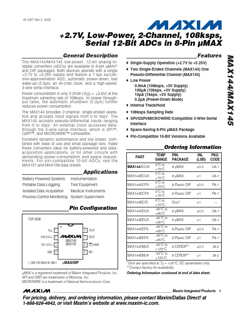
6 5
GND 4
( ) ARE FOR MAX145 ONLY
µMAX/DIP
*Dice are specified at TA = +25°C, DC parameters only. **Contact factory for availability. Ordering Information continued at end of data sheet.
ELECTRICAL CHARACTERISTICS
(V DD = +2.7V to +5.25V, V REF = 2.5V, 0.1µF capacitor at REF, f SCLK = 2.17MHz, 16 clocks/conversion cycle (108ksps), CH- = GND for MAX145, TA = TMIN to TMAX, unless otherwise noted. Typical values are at TA = +25°C.) PARAMETER DC ACCURACY (Note 1) Resolution Relative Accuracy (Note 2) Differential Nonlinearity Offset Error Gain Error Gain Temperature Coefficient Channel-to-Channel Offset Matching Channel-to-Channel Gain Matching (Note 3) ±0.8 ±0.05 ±0.05 RES INL DNL MAX14_A MAX14_B No missing codes over temperature 12 ±0.5 ±1 ±0.75 ±3 ±3 Bits LSB LSB LSB LSB ppm/°C LSB LSB SYMBOL CONDITIONS MIN TYP MAX UNITS
MAX4475

概述MAX4575/MAX4576/MAX4577是低电压,高静电放电(ESD)保护,双单极/单掷(SPST)模拟开关。
常关闭(NO)和常开(NC)引脚对± 15kV的ESD保护而不闭锁或损坏。
每个交换机可以处理轨到轨®模拟信号。
关断漏电流0.5nA在25 ° C。
这些适合低失真音频模拟开关应用和首选的解决方案在自动化测试设备或机械继电器开关电流所需的应用程序。
他们具有低功耗的要求(0.5μW),需要更少的电路板空间,比机械更可靠继电器。
每个设备控制的TTL / CMOS输入电压等级是双边的。
这些开关的功能保证操作+2 V至+12 V单电源供电,使他们的理想使用电池供电的应用。
电阻70Ω(最大),交换机之间的匹配,0.5Ω(典型值)单位在指定的信号范围内(2Ω典型)。
MAX4575有两个无开关,MAX4576两个NC交换机和MAX4577有一个NO和一个NC开关。
这些器件采用8引脚μMAX和SO封装。
应用电池供电系统音频和视频信号路由低电压数据采集系统采样和保持电路通信电路继电器替代品____________________________Features?NO / NC引脚的ESD保护± 15kV的(人体模型)± 15KV(IEC 1000-4-2气隙放电)± 8千伏(IEC 1000-4-2接触放电)?与MAX4541/MAX4542/MAX4543引脚兼容?保证电阻+5 V时的70Ω(最大)在+3 V,150Ω(最大)?通电阻平坦度2Ω(典型值)为+5 V在+3 V,6Ω(典型值)?电阻匹配0.5Ω(典型值)为+5 V在+3 V,0.6Ω(典型值)?保证0.5nA漏电流在TA = +25 ° C?2 V至+12 V单电源电压?TTL / CMOS逻辑兼容?低失真:0.015%?- 3dB带宽> 300MHz的?轨到轨信号范围MAX4575/MAX4576/MAX4577± 15kV ESD保护,低电压,双通道,单刀单掷,CMOS模拟开关______________________________________________________________ __马克西姆综合产品119-1762;冯0 7 / 00;对于免费样品和最新文献,参观访问www.maxim - 或电话1-800-998-8800。
MAX5482ETE+T中文资料

ELECTRICAL CHARACTERISTICS
(VDD = +2.7V to +5.25V, VSS = GND = 0, VH = VDD, VL = 0, TA = -40°C to +85°C, unless otherwise noted. Typical values are at VDD = +5.0V, TA = +25°C, unless otherwise noted.) (Note 1)
Operating Temperature Range ...........................-40°C to +85°C Junction Temperature ......................................................+150°C Storage Temperature Range .............................-60°C to +150°C Lead Temperature (soldering, 10s) .................................+300°C
Applications
Gain and Offset Adjustment
Low-Drift Programmable Gain Amplifiers
LCD Contrast Adjustment Mechanical Potentiometer
Pressure Sensors
Replacement
元器件交易网
19-3708; Rev 4; 12/07
MAX5481–MAX5484
max3485esa中文资料
General Description The MAX3483, MAX3485, MAX3486, MAX3488,MAX3490, and MAX3491 are 3.3V , low-power transceivers forRS-485 and RS-422 communication. Each part containsone driver and one receiver. The MAX3483 and MAX3488feature slew-rate-limited drivers that minimize EMI andreduce reflections caused by improperly terminatedcables, allowing error-free data transmission at data ratesup to 250kbps. The partially slew-rate-limited MAX3486transmits up to 2.5Mbps. The MAX3485, MAX3490, andMAX3491 transmit at up to 10Mbps.Drivers are short-circuit current-limited and are protectedagainst excessive power dissipation by thermal shutdowncircuitry that places the driver outputs into a high-imped-ance state. The receiver input has a fail-safe feature thatguarantees a logic-high output if both inputs are opencircuit.The MAX3488, MAX3490, and MAX3491 feature full-duplex communication, while the MAX3483, MAX3485, andMAX3486 are designed for half-duplex communication.Applications ●Low-Power RS-485/RS-422 Transceivers ●Telecommunications ●Transceivers for EMI-Sensitive Applications ●Industrial-Control Local Area NetworksFeatures●Operate from a Single 3.3V Supply—No Charge Pump!●Interoperable with +5V Logic ●8ns Max Skew (MAX3485/MAX3490/MAX3491)●Slew-Rate Limited for Errorless Data Transmission (MAX3483/MAX3488)●2nA Low-Current Shutdown Mode (MAX3483/MAX3485/MAX3486/MAX3491)●-7V to +12V Common-Mode Input Voltage Range ●Allows up to 32 Transceivers on the Bus ●Full-Duplex and Half-Duplex Versions Available ●Industry Standard 75176 Pinout (MAX3483/MAX3485/MAX3486)●Current-Limiting and Thermal Shutdown for Driver Overload Protection 19-0333; Rev 1; 5/19Ordering Information continued at end of data sheet.*Contact factory for for dice specifications.PARTTEMP . RANGE PIN-PACKAGE MAX3483CPA0°C to +70°C 8 Plastic DIP MAX3483CSA0°C to +70°C 8 SO MAX3483C/D0°C to +70°C Dice*MAX3483EPA-40°C to +85°C 8 Plastic DIP MAX3483ESA-40°C to +85°C 8 SO MAX3485CPA0°C to +70°C 8 Plastic DIP MAX3485CSA0°C to +70°C 8 SO MAX3485C/D0°C to +70°C Dice*MAX3485EPA-40°C to +85°C 8 Plastic DIP MAX3485ESA -40°C to +85°C 8 SO PARTNUMBERGUARANTEED DATA RATE (Mbps)SUPPLY VOLTAGE (V)HALF/FULL DUPLEX SLEW-RATE LIMITED DRIVER/RECEIVER ENABLE SHUTDOWN CURRENT (nA)PIN COUNT MAX34830.25 3.0 to 3.6Half Yes Yes 28MAX348510Half No No 28MAX34862.5Half Yes Yes 28MAX34880.25Half Yes Yes —8MAX349010Half No No —8MAX349110Half No Yes 214MAX3483/MAX3485/MAX3486/MAX3488/MAX3490/MAX3491Selection TableOrdering Information找电子元器件上宇航军工Figure 1. MAX3483/MAX3485/MAX3486 Pin Configuration and Typical Operating Circuit Figure 2. MAX3488/MAX3490 Pin Configuration and Typical Operating Circuit Figure 3. MAX3491 Pin Configuration and Typical Operating CircuitMAX3486/MAX3488/MAX3490/MAX3491True RS-485/RS-422 TransceiversFigure 22. MAX3488/MAX3490/MAX3491 Full-Duplex RS-485 NetworkFigure 23. Line Repeater for MAX3488/MAX3490/MAX3491MAX3486/MAX3488/MAX3490/MAX3491True RS-485/RS-422 Transceivers。
MAX4546CEE-T中文资料

_______________General DescriptionThe MAX4545/MAX4546/MAX4547 are low-voltage T-switches designed for switching RF and video signals from DC to 300MHz in 50Ωand 75Ωsystems. The MAX4545 contains four normally open single-pole/single-throw (SPST) switches. The MAX4546 contains two dual SPST switches (one normally open, one normally closed.)The MAX4547 contains two single-pole/double-throw (SPDT) switches.Each switch is constructed in a “T” configuration, ensuring excellent high-frequency off isolation and crosstalk of -80dB at 10MHz. They can handle Rail-to-Rail ®analog sig-nals in either direction. On-resistance (20Ωmax) is matched between switches to 1Ωmax and is flat (0.5Ωmax) over the specified signal range, using ±5V supplies.The off leakage current is less than 5nA at +25°C and 50nA at +85°C.These CMOS switches can operate with dual power sup-plies ranging from ±2.7V to ±6V or a single supply between +2.7V and +12V. All digital inputs have 0.8V/2.4V logic thresholds, ensuring both TTL- and CMOS-logic com-patibility when using ±5V or a single +5V supply.________________________ApplicationsRF SwitchingVideo Signal RoutingHigh-Speed Data Acquisition Test Equipment ATE Equipment Networking____________________________Featureso Low 50ΩInsertion Loss: -1dB at 100MHz o High 50ΩOff Isolation: -80dB at 10MHz o Low 50ΩCrosstalk: -80dB at 10MHz o DC to 300MHz -3dB Signal Bandwidth o 20ΩSignal Paths with ±5V Supplies o 1ΩSignal-Path Matching with ±5V Supplies o 0.5ΩSignal-Path Flatness with ±5V Supplies o ±2.7V to ±6V Dual Supplies +2.7V to +12V Single Supply o Low Power Consumption: <1µW o Rail-to-Rail Bidirectional Signal Handling o Pin Compatible with Industry-Standard DG540, DG542, DG643o >2kV ESD Protection per Method 3015.7o TTL/CMOS-Compatible Inputs with Single +5V or ±5VMAX4545/MAX4546/MAX4547Quad/Dual, Low-Voltage,Bidirectional RF/Video Switches________________________________________________________________Maxim Integrated Products1_____________________Pin Configurations/Functional Diagrams/Truth Tables19-1232; Rev 0; 6/97Ordering Information continued at end of data sheet.For free samples & the latest literature: , or phone 1-800-998-8800Rail-to-Rail is a registered trademark of Nippon Motorola Ltd.M A X 4545/M A X 4546/M A X 4547Quad/Dual, Low-Voltage,Bidirectional RF/Video Switches 2_______________________________________________________________________________________ABSOLUTE MAXIMUM RATINGSELECTRICAL CHARACTERISTICS—Dual Supplies(V+ = +4.5V to +5.5V, V- = -4.5V to -5.5V, V INL = 0.8V, V INH = 2.4V, V GND_= 0V, T A = T MIN to T MAX , unless otherwise noted. Typical values are at T A = +25°C.)Stresses beyond those listed under “Absolute Maximum Ratings” may cause permanent damage to the device. These are stress ratings only, and functional operation of the device at these or any other conditions beyond those indicated in the operational sections of the specifications is not implied. Exposure to absolute maximum rating conditions for extended periods may affect device reliability.(Voltages Referenced to GND)V+...........................................................................-0.3V, +13.0V V-............................................................................-13.0V, +0.3V V+ to V-...................................................................-0.3V, +13.0V All Other Pins (Note 1)..........................(V- - 0.3V) to (V+ + 0.3V)Continuous Current into Any Terminal..............................±25mA Peak Current into Any Terminal(pulsed at 1ms, 10% duty cycle)..................................±50mA ESD per Method 3015.7..................................................>2000V Continuous Power Dissipation (T A = +70°C) (Note 2)16-Pin Plastic DIP(derate 10.53mW/°C above +70°C)..........................842mW16-Pin Narrow SO(derate 8.70mW/°C above +70°C)............................696mW 16-Pin QSOP (derate 8.3mW/°C above +70°C)..........667mW 20-Pin Plastic DIP (derate 8.0mW/°C above +70°C)...640mW 20-Pin Wide SO (derate 10.00mW/°C above +70°C)..800mW 20-Pin SSOP (derate 8.0mW/°C above +70°C)..........640mW Operating Temperature RangesMAX454_C_ E.....................................................0°C to +70°C MAX454_E_ E..................................................-40°C to +85°C Storage Temperature Range.............................-65°C to +150°C Lead Temperature (soldering, 10sec).............................+300°CNote 1:Voltages on all other pins exceeding V+ or V- are clamped by internal diodes. Limit forward diode current to maximum cur-rent rating.MAX4545/MAX4546/MAX4547Quad/Dual, Low-Voltage,Bidirectional RF/Video Switches_______________________________________________________________________________________3ELECTRICAL CHARACTERISTICS—Dual Supplies (continued)(V+ = +4.5V to +5.5V, V- = -4.5V to -5.5V, V INL = 0.8V, V INH = 2.4V, V GND_= 0V, T A = T MIN to T MAX , unless otherwise noted. Typical values are at T A = +25°C.)M A X 4545/M A X 4546/M A X 4547Quad/Dual, Low-Voltage,Bidirectional RF/Video Switches 4_______________________________________________________________________________________ELECTRICAL CHARACTERISTICS—Single +5V Supply(V+ = +4.5V to +5.5V, V- = 0V, V INL = 0.8V, V INH = 2.4V, V GND_= 0V, T A = T MIN to T MAX , unless otherwise noted. Typical values are at T A = +25°C.)MAX4545/MAX4546/MAX4547Quad/Dual, Low-Voltage,Bidirectional RF/Video Switches_______________________________________________________________________________________5ELECTRICAL CHARACTERISTICS—Single +3V Supply(V+ = +2.7V to +3.6V, V- = 0V, V INL = 0.8V, V INH = 2.4V, V GND_ = 0V, T A = T MIN to T MAX , unless otherwise noted. Typical values are at T A = +25°C.)Note 2:The algebraic convention is used in this data sheet; the most negative value is shown in the minimum column.Note 3:Guaranteed by design.Note 4:∆R ON = ∆R ON(MAX)- ∆R ON(MIN).Note 5:Resistance flatness is defined as the difference between the maximum and the minimum value of on-resistance as mea-sured over the specified analog signal range.Note 6:Leakage parameters are 100% tested at the maximum rated hot temperature and guaranteed by correlation at +25°C.Note 7:Off isolation = 20log 10[V COM / (V NC or V NO )], V COM = output, V NC or V NO = input to off switch.Note 8:Between any two switches.Note 9:Leakage testing for single-supply operation is guaranteed by testing with dual supplies.M A X 4545/M A X 4546/M A X 4547Quad/Dual, Low-Voltage,Bidirectional RF/Video Switches 6_________________________________________________________________________________________________________________________________Typical Operating Characteristics(V+ = +5V, V- = -5V, T A = +25°C, GND = 0V, packages are surface mount, unless otherwise noted.)10010-51234-4-3-2-15ON-RESISTANCE vs. V COM(DUAL SUPPLIES)V COM (V)R O N (Ω)5111315971723192125-5-3-2-4-1012345ON-RESISTANCE vs. V COM AND TEMPERATURE (DUAL SUPPLIES)V COM (V)R O N (Ω)10001010012345678910ON-RESISTANCE vs. V COM(SINGLE SUPPLY)V COM (V)R O N (Ω)102025153040354501.0 1.50.52.0 2.53.0 3.54.0 4.55.0ON-RESISTANCE vs. V COM AND TEMPERATURE (SINGLE SUPPLY)V COM (V)R O N (Ω)050100150200250±2±3±4±5±6±8ON/OFF TIME vs.SUPPLY VOLTAGEM A X 4545 T O C 07V+, V- (V)t O N , t O F F (n s )t ONt OFF0.00010.0010.010.1110-75-50-25257550100125ON/OFF-LEAKAGE CURRENT vs.TEMPERATURETEMPERATURE (°C)L E A K A G E (n A)-20204006010080120-5-3-2-4-1012345CHARGE INJECTION vs. V COMV COM (V)Q j (p C )103050709011020406080100-75-2575125-502550100ON/OFF TIME vs.TEMPERATUREM A X 4545 T O C 08TEMPERATURE (°C)t O N , t O F F (n s )t ONt OFF0.000010.00010.001I-I+0.010.11-75-2575125-502550100POWER-SUPPLY CURRENT vs. TEMPERATUREM A X 4545 T O C 09TEMPERATURE (°C)I +, I - (µA )MAX4545/MAX4546/MAX4547Quad/Dual, Low-Voltage,Bidirectional RF/Video Switches_______________________________________________________________________________________70.40.20.61.21.41.00.81.601.0 1.52.0 2.50.53.0 3.54.0 4.55.0LOGIC-LEVEL THRESHOLD vs. POSITIVE SUPPLY VOLTAGEM A X 4545 T O C 10V+ (V)L O G I C -L E V E L T H R E S H O L D (V )-1200.11010001001MAX4545FREQUENCY RESPONSE-100-110FREQUENCY (MHz)L O S S (d B )-80-90-60-50-70-40-20-10-30-1001101001000MAX4546FREQUENCY RESPONSE-60-70-80-90-30-40-50-20-10FREQUENCY (MHz)L O S S (d B )100-20-10-1001101000FREQUENCY RESPONSE-70-80-90-30-40-50-601006080-100-40-60-8040200-20FREQUENCY (MHz)S W I T C H L O S S (d B )O N P H A S E (D E G R E E S )1001000.0001101k 100k10k100MAX4547TOTAL HARMONIC DISTORTIONvs. FREQUENCY0.001FREQUENCY (Hz)T H D (%)0.010.1110____________________________Typical Operating Characteristics (continued)(V+ = +5V, V- = -5V, T A = +25°C, GND = 0V, packages are surface mount, unless otherwise noted.)_______________Theory of OperationLogic-Level TranslatorsThe MAX4545/MAX4546/MAX4547 are constructed as high-frequency “T” switches, as shown in Figure 1. The logic-level input, IN_, is translated by amplifier A1 into a V+ to V- logic signal that drives amplifier A2. (Amplifier A2 is an inverter for normally closed switches.)Amplifier A2 drives the gates of N-channel MOSFETs N1 and N2 from V+ to V-, turning them fully on or off.The same signal drives inverter A3 (which drives the P-channel MOSFETs P1 and P2) from V+ to V-, turning them fully on or off, and drives the N-channel MOSFET N3 off and on.The logic-level threshold is determined by V+ and GND_. The voltage on GND_ is usually at ground potential, but it may be set to any voltage between (V+ - 2V) and V-. When the voltage between V+ and GND_ is less than 2V, the level translators become very slow and unreliable. Since individual switches in each package have individual GND_ pins, they may be set to different voltages. Normally, however, they should all be connected to the ground plane.Switch On ConditionWhen the switch is on, MOSFETs N1, N2, P1, and P2are on and MOSFET N3 is off. The signal path is COM_to NO_, and because both N-channel and P-channel MOSFETs act as pure resistances, it is symmetrical(i.e., signals may pass in either direction). The off MOSFET, N3, has no DC conduction, but has a small amount of capacitance to GND_. The four on MOSFETs also have capacitance to ground that,together with the series resistance, forms a lowpass fil-ter. All of these capacitances are distributed evenly along the series resistance, so they act as a transmis-sion line rather than a simple R-C filter. This helps to explain the exceptional 300MHz bandwidth when the switches are on.M A X 4545/M A X 4546/M A X 4547Quad/Dual, Low-Voltage,Bidirectional RF/Video Switches 8_____________________________________________________________________________________________________________________________________________________Pin Description*All pins have ESD diodes to V- and V+.**NO_ (or NC_) and COM_ pins are identical and interchangeable. Either may be considered as an input or output; signals passequally well in either direction.Figure 1. T-Switch ConstructionTypical attenuation in 50Ωsystems is -1dB and is rea-sonably flat up to 100MHz. Higher-impedance circuits show even lower attenuation (and vice versa), but slightly lower bandwidth due to the increased effect of the internal and external capacitance and the switch’s internal resistance.The MAX4545/MAX4546/MAX4547 are optimized for ±5V operation. Using lower supply voltages or a single supply increases switching time, increases on-resis-tance (and therefore on-state attenuation), and increas-es nonlinearity.Switch Off Condition When the switch is off, MOSFETs N1, N2, P1, and P2 are off and MOSFET N3 is on. The signal path is through the off-capacitances of the series MOSFETs, but it is shunted to ground by N3. This forms a high-pass filter whose exact characteristics are dependent on the source and load impedances. In 50Ωsystems, and below 10MHz, the attenuation can exceed 80dB. This value decreases with increasing frequency and increasing circuit impedances. External capacitance and board layout have a major role in determining over-all performance.__________Applications InformationPower-Supply ConsiderationsOverview The MAX4545/MAX4546/MAX4547 construction is typi-cal of most CMOS analog switches. It has three supply pins: V+, V-, and GND. V+ and V- are used to drive the internal CMOS switches and set the limits of the analog voltage on any switch. Reverse ESD protection diodes are internally connected between each analog signal pin and both V+ and V-. If the voltage on any pin exceeds V+ or V-, one of these diodes will conduct. During normal operation these reverse-biased ESD diodes leak, forming the only current drawn from V-. Virtually all the analog leakage current is through the ESD diodes. Although the ESD diodes on a given sig-nal pin are identical, and therefore fairly well balanced, they are reverse biased differently. Each is biased by either V+ or V- and the analog signal. This means their leakages vary as the signal varies. The difference in the two diode leakages from the signal path to the V+ and V- pins constitutes the analog signal-path leakage cur-rent. All analog leakage current flows to the supply ter-minals, not to the other switch terminal. This explains how both sides of a given switch can show leakage currents of either the same or opposite polarity.There is no connection between the analog signal paths and GND. The analog signal paths consist of an N-channel and P-channel MOSFET with their sources and drains paralleled and their gates driven out of phase with V+ and V- by the logic-level translators.V+ and GND power the internal logic and logic-level translators, and set the input logic thresholds. The logic-level translators convert the logic levels to switched V+ and V- signals to drive the gates of the analog switches. This drive signal is the only connec-tion between the logic supplies and the analog sup-plies. All pins have ESD protection to V+ and to V-. Increasing V- has no effect on the logic-level thresh-olds, but it does increase the drive to the P-channel switches, reducing their on-resistance. V- also sets the negative limit of the analog signal voltage.The logic-level thresholds are CMOS and TTL compati-ble when V+ is +5V. As V+ is raised, the threshold increases slightly; when V+ reaches +12V, the level threshold is about 3.1V, which is above the TTL output high-level minimum of 2.8V, but still compatible with CMOS outputs.Bipolar-Supply Operation The MAX4545/MAX4546/MAX4547 operate with bipolar supplies between ±2.7V and ±6V. The V+ and V- sup-plies need not be symmetrical, but their sum cannot exceed the absolute maximum rating of 13.0V. Do not connect the MAX4545/MAX4546/MAX4547 V+ pin to +3V and connect the logic-level input pins to TTL logic-level signals. TTL logic-level outputs can exceed the absolute maximum ratings, causing damage to the part and/or external circuits.CAUTION:The absolute maximum V+ to V- differential voltage is 13.0V. Typical “±6-Volt” or “12-Volt”supplies with ±10% tolerances can be as high as 13.2V. This voltage can damage the MAX4545/MAX4546/MAX4547. Even ±5% toler-ance supplies may have overshoot or noise spikes that exceed 13.0V.Single-Supply Operation The MAX4545/MAX4546/MAX4547 operate from a sin-gle supply between +2.7V and +12V when V- is con-nected to GND. All of the bipolar precautions must be observed. Note, however, that these parts are opti-mized for ±5V operation, and most AC and DC charac-teristics are degraded significantly when departing from ±5V. As the overall supply voltage (V+ to V-) is lowered, switching speed, on-resistance, off isolation, and distortion are degraded. (See Typical Operating Characteristics.) MAX4545/MAX4546/MAX4547Quad/Dual, Low-Voltage,Bidirectional RF/Video Switches _______________________________________________________________________________________9M A X 4545/M A X 4546/M A X 4547Single-supply operation also limits signal levels and interferes with grounded signals. When V- = 0V, AC sig-nals are limited to -0.3V. Voltages below -0.3V can be clipped by the internal ESD-protection diodes, and the parts can be damaged if excessive current flows.Power OffWhen power to the MAX4545/MAX4546/MAX4547 is off (i.e., V+ = 0V and V- = 0V), the Absolute Maximum Ratings still apply. This means that neither logic-level inputs on IN_ nor signals on COM_, NO_, or NC_ can exceed ±0.3V. Voltages beyond ±0.3V cause the inter-nal ESD-protection diodes to conduct, and the parts can be damaged if excessive current flows.GroundingDC Ground ConsiderationsSatisfactory high-frequency operation requires that careful consideration be given to grounding. For most applications, a ground plane is strongly recom-mended, and all GND_ pins should be connected to it with solid copper.While the V+ and V- power-supply pins are common to all switches in a given package,each switch has separate ground pins that are not internally connected to each other. This contributes to the overall high-frequency performance and provides added flexibility in some applications, but it can cause problems if it is overlooked. All the GND_ pins have ESD diodes to V+ and V-.In systems that have separate digital and analog (sig-nal) grounds, connect these switch GND_ pins to ana-log ground. Preserving a good signal ground is much more important than preserving a digital ground.Ground current is only a few nanoamps.The logic-level inputs, IN_, have voltage thresholds determined by V+ and GND_. (V- does not influence the logic-level threshold.) With +5V and 0V applied to V+ and GND_, the threshold is about 1.6V, ensuring compatibility with TTL- and CMOS-logic drivers.The various GND_ pins can be connected to separate voltage potentials if any or all of the logic-level inputs is not a normal logic signal. (The GND_ voltages cannot exceed (V+ - 2V) or V-.) Elevating GND_ reduces off isolation. For example, using the MAX4545, if GND2–GND6 are connected to 0V and GND1 is connected to V-, then switches 2, 3, and 4 would be TTL/CMOS com-patible, but switch 1 (IN1) could be driven with the rail-to-rail output of an op amp operating from V+ and V-.Note, however, that IN_ can be driven more negative than GND_, as far as V-. GND_ does not have to be removed from 0V when IN_ is driven from bipolar sources, but the voltage on IN_ should never exceed V-.GND_ should be separated from 0V only if the logic-level threshold has to be changed.Any GND_ pin not connected to 0V should be bypassed to the ground plane with a surface-mount 10nF capacitor to maintain good RF grounding. DC current in the IN_ and GND_ pins is less than 1nA, but increases with switching frequency.On the MAX4545 only, two extra ground pins—GND5and GND6—are provided to improve isolation and crosstalk. They are not connected to the logic-level cir-cuit. These pins should always be connected to the ground plane with solid copper.AC Ground and BypassingA ground plane is mandatory for satisfactory high-frequency operation.(Prototyping using hand wiring or wire-wrap boards is strongly discouraged.) Connect all 0V GND_ pins to the ground plane with solid copper.(The GND_ pins extend the high-frequency ground through the package wire-frame, into the silicon itself,thus improving isolation.) The ground plane should be solid metal underneath the device, without interruptions.There should be no traces under the device itself. For DIP packages, this applies to both sides of a two-sided board. Failure to observe this will have a minimal effect on the “on” characteristics of the switch at high frequen-cies, but it will degrade the off isolation and crosstalk.All V+ and V- pins should be bypassed to the ground plane with surface-mount 10nF capacitors. For DIP packages, they should be mounted as close as possi-ble to the pins on the same side of the board as the device. Do not use feedthroughs or vias for bypass capacitors. For surface-mount packages, the pins are so close to each other that the bypass capacitors should be mounted on the opposite side of the board from the device. In this case, use short feedthroughs or vias, directly under the V+ and V- pins. Any GND_ pin not connected to 0V should be similarly bypassed. If V-is 0V, connect it directly to the ground plane with solid copper. Keep all leads short.The MAX4547 has two V+ and V- pins. Make DC con-nections to only one of each to minimize crosstalk. Do not route DC current into one of the V+ or V- pins and out the other V+ or V- pin to other devices. The second set of V+ and V- pins is for AC bypassing only.For dual-supply operation, the MAX4547 should have four 10nF bypass capacitors connected to each V+and V- pin, as close to the package as possible. For single-supply operation, the MAX4547 should have two 10nF bypass capacitors connected (one to each V+pin), as close to the package as possible.Quad/Dual, Low-Voltage,Bidirectional RF/Video Switches 10______________________________________________________________________________________MAX4545/MAX4546/MAX4547Bidirectional RF/Video Switches______________________________________________________________________________________11On the MAX4545, GND5 and GND6 should always be connected to the ground plane with solid copper to improve isolation and crosstalk.Signal RoutingKeep all signal leads as short as possible. Separate all signal leads from each other and other traces with the ground plane on both sides of the board. Where possi-ble, use coaxial cable instead of printed circuit board traces.Board LayoutIC sockets degrade high-frequency performance and should not be used if signal bandwidth exceeds 5MHz.Surface-mount parts, having shorter internal lead frames, provide the best high-frequency performance.Keep all bypass capacitors close to the device, and separate all signal leads with ground planes. Such grounds tend to be wedge-shaped as they get closer to the device. Use vias to connect the ground planes on each side of the board, and place the vias in the apex of the wedge-shaped grounds that separate signal leads.Logic-level signal lead placement is not critical.Impedance MatchingThe typical on-resistances of the switches in the MAX4545/MAX4546/MAX4547 are 14Ω, but the off-state impedances are approximately equal to a 6pF capacitor. In coaxial systems, therefore, it is impossible to match any impedance for both the on and off state. If impedance matching is critical, the MAX4546 is best suited, since its two sections can be configured as a single on/off switch, as shown in Figure 2. This circuit “wastes” switches and has higher losses, but has bet-ter off isolation and maintains good impedance match-ing in both the on and off states. The resistance values shown in Figure 3 are optimized with ±5V supplies for both 50Ωand 75Ωsystems at room temperature.MultiplexerWith its excellent off isolation, the MAX4545 is ideal for use in high-frequency video multiplexers. Figure 3shows such an application for switching any one of four video inputs to a single output. The same circuit may be used as a demultiplexer by simply reversing the sig-nal direction.Stray capacitance of traces and the output capacitance of switches placed in parallel reduces bandwidth, so the outputs of no more than four individual switches should be placed in parallel if high bandwidth is to be main-tained. If more than four mux channels are needed, the 4-channel circuit should be duplicated and cascaded.Figure 2. Impedance Matching On/Off SwitchM A X 4545/M A X 4546/M A X 4547Bidirectional RF/Video Switches 12______________________________________________________________________________________Figure 3. 4-Channel MultiplexerMAX4545/MAX4546/MAX4547Bidirectional RF/Video Switches______________________________________________________________________________________13Figure 4. Switching Time______________________________________________Test Circuits/Timing DiagramsFigure 5. Break-Before-Make Interval (MAX4546/MAX4547 only)M A X 4545/M A X 4546/M A X 4547Bidirectional RF/Video Switches 14______________________________________________________________________________________Figure 6. Charge InjectionFigure 7. On Loss, Off Isolation, and Crosstalk_________________________________Test Circuits/Timing Diagrams (continued)MAX4545/MAX4546/MAX4547Bidirectional RF/Video Switches______________________________________________________________________________________15N.C. = NO INTERNAL CONNECTIONTRANSISTOR COUNT: 253SUBSTRATE INTERNALLY CONNECTED TO V-GND2GND5GND4NO4V-NO1COM30.101"(2.565mm)0.085"(2.159mm)COM4IN4IN3GND6V+NO2N.C.NO3GND3COM1IN1IN2COM2GND1N.C.MAX4545GND2GND4N.C.COM1N.C.N.C.NC20.101"(2.565mm)0.085"(2.159mm)V+NC1IN2COM2N.C.N.C.V-N.C.GND3GND1V-MAX4547GND2N.C.N.C.NC4V-NO1GND30.101"(2.565mm)MAX4546GND4COM4COM3N.C.V+NO2N.C.NC30.085"(2.159mm)GND1N.C.Figure 8. NO_, NC_, COM_ Capacitance_________________Chip TopographiesMaxim cannot assume responsibility for use of any circuitry other than circuitry entirely embodied in a Maxim product. No circuit patent licenses are implied. Maxim reserves the right to change the circuitry and specifications without notice at any time.16__________________Maxim Integrated Products, 120 San Gabriel Drive, Sunnyvale, CA 94086 (408) 737-7600©1997 Maxim Integrated ProductsPrinted USAis a registered trademark of Maxim Integrated Products.M A X 4545/M A X 4546/M A X 4547Bidirectional RF/Video Switches___________________________________________Ordering Information (continued)*Contact factory for dice specifications.。
MAX487ESA中文资料
For pricing, delivery, and ordering information,please contact Maxim/Dallas Direct!at 1-888-629-4642, or visit Maxim’s website at .General DescriptionThe MAX481, MAX483, MAX485, MAX487–MAX491, and MAX1487 are low-power transceivers for RS-485 and RS-422 communication. Each part contains one driver and one receiver. The MAX483, MAX487, MAX488, and MAX489feature reduced slew-rate drivers that minimize EMI and reduce reflections caused by improperly terminated cables,thus allowing error-free data transmission up to 250kbps.The driver slew rates of the MAX481, MAX485, MAX490,MAX491, and MAX1487 are not limited, allowing them to transmit up to 2.5Mbps.These transceivers draw between 120µA and 500µA of supply current when unloaded or fully loaded with disabled drivers. Additionally, the MAX481, MAX483, and MAX487have a low-current shutdown mode in which they consume only 0.1µA. All parts operate from a single 5V supply.Drivers are short-circuit current limited and are protected against excessive power dissipation by thermal shutdown circuitry that places the driver outputs into a high-imped-ance state. The receiver input has a fail-safe feature that guarantees a logic-high output if the input is open circuit.The MAX487 and MAX1487 feature quarter-unit-load receiver input impedance, allowing up to 128 MAX487/MAX1487 transceivers on the bus. Full-duplex communi-cations are obtained using the MAX488–MAX491, while the MAX481, MAX483, MAX485, MAX487, and MAX1487are designed for half-duplex applications.________________________ApplicationsLow-Power RS-485 Transceivers Low-Power RS-422 Transceivers Level TranslatorsTransceivers for EMI-Sensitive Applications Industrial-Control Local Area Networks__Next Generation Device Features♦For Fault-Tolerant ApplicationsMAX3430: ±80V Fault-Protected, Fail-Safe, 1/4Unit Load, +3.3V, RS-485 TransceiverMAX3440E–MAX3444E: ±15kV ESD-Protected,±60V Fault-Protected, 10Mbps, Fail-Safe, RS-485/J1708 Transceivers♦For Space-Constrained ApplicationsMAX3460–MAX3464: +5V, Fail-Safe, 20Mbps,Profibus RS-485/RS-422 TransceiversMAX3362: +3.3V, High-Speed, RS-485/RS-422Transceiver in a SOT23 PackageMAX3280E–MAX3284E: ±15kV ESD-Protected,52Mbps, +3V to +5.5V, SOT23, RS-485/RS-422,True Fail-Safe ReceiversMAX3293/MAX3294/MAX3295: 20Mbps, +3.3V,SOT23, RS-855/RS-422 Transmitters ♦For Multiple Transceiver ApplicationsMAX3030E–MAX3033E: ±15kV ESD-Protected,+3.3V, Quad RS-422 Transmitters ♦For Fail-Safe ApplicationsMAX3080–MAX3089: Fail-Safe, High-Speed (10Mbps), Slew-Rate-Limited RS-485/RS-422Transceivers♦For Low-Voltage ApplicationsMAX3483E/MAX3485E/MAX3486E/MAX3488E/MAX3490E/MAX3491E: +3.3V Powered, ±15kV ESD-Protected, 12Mbps, Slew-Rate-Limited,True RS-485/RS-422 TransceiversMAX481/MAX483/MAX485/MAX487–MAX491/MAX1487Low-Power, Slew-Rate-Limited RS-485/RS-422 Transceivers______________________________________________________________Selection Table19-0122; Rev 8; 10/03Ordering Information appears at end of data sheet.M A X 481/M A X 483/M A X 485/M A X 487–M A X 491/M A X 1487Low-Power, Slew-Rate-Limited RS-485/RS-422 Transceivers 2_______________________________________________________________________________________ABSOLUTE MAXIMUM RATINGSSupply Voltage (V CC ).............................................................12V Control Input Voltage (RE , DE)...................-0.5V to (V CC + 0.5V)Driver Input Voltage (DI).............................-0.5V to (V CC + 0.5V)Driver Output Voltage (A, B)...................................-8V to +12.5V Receiver Input Voltage (A, B).................................-8V to +12.5V Receiver Output Voltage (RO).....................-0.5V to (V CC +0.5V)Continuous Power Dissipation (T A = +70°C)8-Pin Plastic DIP (derate 9.09mW/°C above +70°C)....727mW 14-Pin Plastic DIP (derate 10.00mW/°C above +70°C)..800mW 8-Pin SO (derate 5.88mW/°C above +70°C).................471mW14-Pin SO (derate 8.33mW/°C above +70°C)...............667mW 8-Pin µMAX (derate 4.1mW/°C above +70°C)..............830mW 8-Pin CERDIP (derate 8.00mW/°C above +70°C).........640mW 14-Pin CERDIP (derate 9.09mW/°C above +70°C).......727mW Operating Temperature RangesMAX4_ _C_ _/MAX1487C_ A...............................0°C to +70°C MAX4__E_ _/MAX1487E_ A.............................-40°C to +85°C MAX4__MJ_/MAX1487MJA...........................-55°C to +125°C Storage Temperature Range.............................-65°C to +160°C Lead Temperature (soldering, 10sec).............................+300°CDC ELECTRICAL CHARACTERISTICS(V CC = 5V ±5%, T A = T MIN to T MAX , unless otherwise noted.) (Notes 1, 2)Stresses beyond those listed under “Absolute Maximum Ratings” may cause permanent damage to the device. These are stress ratings only, and functional operation of the device at these or any other conditions beyond those indicated in the operational sections of the specifications is not implied. Exposure to absolute maximum rating conditions for extended periods may affect device reliability.V V IN = -7VV IN = 12V V IN = -7V V IN = 12V Input Current (A, B)I IN2V TH k Ω48-7V ≤V CM ≤12V, MAX487/MAX1487R INReceiver Input Resistance -7V ≤V CM ≤12V, all devices except MAX487/MAX1487R = 27Ω(RS-485), Figure 40.4V ≤V O ≤2.4VR = 50Ω(RS-422)I O = 4mA, V ID = -200mV I O = -4mA, V ID = 200mV V CM = 0V-7V ≤V CM ≤12V DE, DI, RE DE, DI, RE MAX487/MAX1487,DE = 0V, V CC = 0V or 5.25VDE, DI, RE R = 27Ωor 50Ω, Figure 4R = 27Ωor 50Ω, Figure 4R = 27Ωor 50Ω, Figure 4DE = 0V;V CC = 0V or 5.25V,all devices except MAX487/MAX1487CONDITIONSk Ω12µA ±1I OZRThree-State (high impedance)Output Current at ReceiverV 0.4V OL Receiver Output Low Voltage 3.5V OH Receiver Output High Voltage mV 70∆V TH Receiver Input Hysteresis V -0.20.2Receiver Differential Threshold Voltage-0.2mA 0.25mA-0.81.01.55V OD2Differential Driver Output (with load)V 2V 5V OD1Differential Driver Output (no load)µA±2I IN1Input CurrentV 0.8V IL Input Low Voltage V 2.0V IH Input High Voltage V 0.2∆V OD Change in Magnitude of Driver Common-Mode Output Voltage for Complementary Output States V 0.2∆V OD Change in Magnitude of Driver Differential Output Voltage for Complementary Output States V 3V OC Driver Common-Mode Output VoltageUNITS MINTYPMAX SYMBOL PARAMETERMAX481/MAX483/MAX485/MAX487–MAX491/MAX1487Low-Power, Slew-Rate-Limited RS-485/RS-422 Transceivers_______________________________________________________________________________________3SWITCHING CHARACTERISTICS—MAX481/MAX485, MAX490/MAX491, MAX1487(V CC = 5V ±5%, T A = T MIN to T MAX , unless otherwise noted.) (Notes 1, 2)DC ELECTRICAL CHARACTERISTICS (continued)(V CC = 5V ±5%, T A = T MIN to T MAX , unless otherwise noted.) (Notes 1, 2)ns 103060t PHLDriver Rise or Fall Time Figures 6 and 8, R DIFF = 54Ω, C L1= C L2= 100pF ns MAX490M, MAX491M MAX490C/E, MAX491C/E2090150MAX481, MAX485, MAX1487MAX490M, MAX491MMAX490C/E, MAX491C/E MAX481, MAX485, MAX1487Figures 6 and 8, R DIFF = 54Ω,C L1= C L2= 100pF MAX481 (Note 5)Figures 5 and 11, C RL = 15pF, S2 closedFigures 5 and 11, C RL = 15pF, S1 closed Figures 5 and 11, C RL = 15pF, S2 closed Figures 5 and 11, C RL = 15pF, S1 closed Figures 6 and 10, R DIFF = 54Ω,C L1= C L2= 100pFFigures 6 and 8,R DIFF = 54Ω,C L1= C L2= 100pF Figures 6 and 10,R DIFF = 54Ω,C L1= C L2= 100pF CONDITIONS ns 510t SKEW ns50200600t SHDNTime to ShutdownMbps 2.5f MAX Maximum Data Rate ns 2050t HZ Receiver Disable Time from High ns 103060t PLH 2050t LZ Receiver Disable Time from Low ns 2050t ZH Driver Input to Output Receiver Enable to Output High ns 2050t ZL Receiver Enable to Output Low 2090200ns ns 134070t HZ t SKD Driver Disable Time from High |t PLH - t PHL |DifferentialReceiver Skewns 4070t LZ Driver Disable Time from Low ns 4070t ZL Driver Enable to Output Low 31540ns51525ns 31540t R , t F 2090200Driver Output Skew to Output t PLH , t PHL Receiver Input to Output4070t ZH Driver Enable to Output High UNITS MIN TYP MAX SYMBOL PARAMETERFigures 7 and 9, C L = 100pF, S2 closed Figures 7 and 9, C L = 100pF, S1 closed Figures 7 and 9, C L = 15pF, S1 closed Figures 7 and 9, C L = 15pF, S2 closedM A X 481/M A X 483/M A X 485/M A X 487–M A X 491/M A X 1487Low-Power, Slew-Rate-Limited RS-485/RS-422 Transceivers 4_______________________________________________________________________________________SWITCHING CHARACTERISTICS—MAX483, MAX487/MAX488/MAX489(V CC = 5V ±5%, T A = T MIN to T MAX , unless otherwise noted.) (Notes 1, 2)SWITCHING CHARACTERISTICS—MAX481/MAX485, MAX490/MAX491, MAX1487 (continued)(V CC = 5V ±5%, T A = T MIN to T MAX , unless otherwise noted.) (Notes 1, 2)3001000Figures 7 and 9, C L = 100pF, S2 closed Figures 7 and 9, C L = 100pF, S1 closed Figures 5 and 11, C L = 15pF, S2 closed,A - B = 2VCONDITIONSns 40100t ZH(SHDN)Driver Enable from Shutdown toOutput High (MAX481)nsFigures 5 and 11, C L = 15pF, S1 closed,B - A = 2Vt ZL(SHDN)Receiver Enable from Shutdownto Output Low (MAX481)ns 40100t ZL(SHDN)Driver Enable from Shutdown toOutput Low (MAX481)ns 3001000t ZH(SHDN)Receiver Enable from Shutdownto Output High (MAX481)UNITS MINTYP MAX SYMBOLPARAMETERt PLH t SKEW Figures 6 and 8, R DIFF = 54Ω,C L1= C L2= 100pFt PHL Figures 6 and 8, R DIFF = 54Ω,C L1= C L2= 100pFDriver Input to Output Driver Output Skew to Output ns 100800ns ns 2000MAX483/MAX487, Figures 7 and 9,C L = 100pF, S2 closedt ZH(SHDN)Driver Enable from Shutdown to Output High2502000ns2500MAX483/MAX487, Figures 5 and 11,C L = 15pF, S1 closedt ZL(SHDN)Receiver Enable from Shutdown to Output Lowns 2500MAX483/MAX487, Figures 5 and 11,C L = 15pF, S2 closedt ZH(SHDN)Receiver Enable from Shutdown to Output Highns 2000MAX483/MAX487, Figures 7 and 9,C L = 100pF, S1 closedt ZL(SHDN)Driver Enable from Shutdown to Output Lowns 50200600MAX483/MAX487 (Note 5) t SHDN Time to Shutdownt PHL t PLH , t PHL < 50% of data period Figures 5 and 11, C RL = 15pF, S2 closed Figures 5 and 11, C RL = 15pF, S1 closed Figures 5 and 11, C RL = 15pF, S2 closed Figures 5 and 11, C RL = 15pF, S1 closed Figures 7 and 9, C L = 15pF, S2 closed Figures 6 and 10, R DIFF = 54Ω,C L1= C L2= 100pFFigures 7 and 9, C L = 15pF, S1 closed Figures 7 and 9, C L = 100pF, S1 closed Figures 7 and 9, C L = 100pF, S2 closed CONDITIONSkbps 250f MAX 2508002000Maximum Data Rate ns 2050t HZ Receiver Disable Time from High ns 25080020002050t LZ Receiver Disable Time from Low ns 2050t ZH Receiver Enable to Output High ns 2050t ZL Receiver Enable to Output Low ns ns 1003003000t HZ t SKD Driver Disable Time from High I t PLH - t PHL I DifferentialReceiver SkewFigures 6 and 10, R DIFF = 54Ω,C L1= C L2= 100pFns 3003000t LZ Driver Disable Time from Low ns 2502000t ZL Driver Enable to Output Low ns Figures 6 and 8, R DIFF = 54Ω,C L1= C L2= 100pFns 2502000t R , t F 2502000Driver Rise or Fall Time ns t PLH Receiver Input to Output2502000t ZH Driver Enable to Output High UNITS MIN TYP MAX SYMBOL PARAMETERMAX481/MAX483/MAX485/MAX487–MAX491/MAX1487Low-Power, Slew-Rate-Limited RS-485/RS-422 Transceivers_______________________________________________________________________________________530002.5OUTPUT CURRENT vs.RECEIVER OUTPUT LOW VOLTAGE525M A X 481-01OUTPUT LOW VOLTAGE (V)O U T P U T C U R R E N T (m A )1.515100.51.02.0203540450.90.1-50-252575RECEIVER OUTPUT LOW VOLTAGE vs.TEMPERATURE0.30.7TEMPERATURE (°C)O U T P U TL O W V O L T A G E (V )500.50.80.20.60.40100125-20-41.5 2.0 3.0 5.0OUTPUT CURRENT vs.RECEIVER OUTPUT HIGH VOLTAGE-8-16M A X 481-02OUTPUT HIGH VOLTAGE (V)O U T P U T C U R R E N T (m A )2.5 4.0-12-18-6-14-10-203.54.5 4.83.2-50-252575RECEIVER OUTPUT HIGH VOLTAGE vs.TEMPERATURE3.64.4TEMPERATURE (°C)O U T P UT H I G H V O L T A G E (V )0504.04.63.44.23.83.01001259000 1.0 3.0 4.5DRIVER OUTPUT CURRENT vs.DIFFERENTIAL OUTPUT VOLTAGE1070M A X 481-05DIFFERENTIAL OUTPUT VOLTAGE (V)O U T P U T C U R R E N T (m A )2.0 4.05030806040200.5 1.5 2.53.5 2.31.5-50-2525125DRIVER DIFFERENTIAL OUTPUT VOLTAGEvs. TEMPERATURE1.72.1TEMPERATURE (°C)D I F FE R E N T I A L O U T P U T V O L T A G E (V )751.92.21.62.01.8100502.4__________________________________________Typical Operating Characteristics(V CC = 5V, T A = +25°C, unless otherwise noted.)NOTES FOR ELECTRICAL/SWITCHING CHARACTERISTICSNote 1:All currents into device pins are positive; all currents out of device pins are negative. All voltages are referenced to deviceground unless otherwise specified.Note 2:All typical specifications are given for V CC = 5V and T A = +25°C.Note 3:Supply current specification is valid for loaded transmitters when DE = 0V.Note 4:Applies to peak current. See Typical Operating Characteristics.Note 5:The MAX481/MAX483/MAX487 are put into shutdown by bringing RE high and DE low. If the inputs are in this state for lessthan 50ns, the parts are guaranteed not to enter shutdown. If the inputs are in this state for at least 600ns, the parts are guaranteed to have entered shutdown. See Low-Power Shutdown Mode section.M A X 481/M A X 483/M A X 485/M A X 487–M A X 491/M A X 1487Low-Power, Slew-Rate-Limited RS-485/RS-422 Transceivers 6___________________________________________________________________________________________________________________Typical Operating Characteristics (continued)(V CC = 5V, T A = +25°C, unless otherwise noted.)120008OUTPUT CURRENT vs.DRIVER OUTPUT LOW VOLTAGE20100M A X 481-07OUTPUT LOW VOLTAGE (V)O U T P U T C U R R E N T (m A )6604024801012140-1200-7-5-15OUTPUT CURRENT vs.DRIVER OUTPUT HIGH VOLTAGE-20-80M A X 481-08OUTPUT HIGH VOLTAGE (V)O U T P U T C U R R E N T (m A )-31-603-6-4-2024-100-40100-40-60-2040100120MAX1487SUPPLY CURRENT vs. TEMPERATURE300TEMPERATURE (°C)S U P P L Y C U R R E N T (µA )20608050020060040000140100-50-2550100MAX481/MAX485/MAX490/MAX491SUPPLY CURRENT vs. TEMPERATURE300TEMPERATURE (°C)S U P P L Y C U R R E N T (µA )257550020060040000125100-50-2550100MAX483/MAX487–MAX489SUPPLY CURRENT vs. TEMPERATURE300TEMPERATURE (°C)S U P P L Y C U R R E N T (µA )257550020060040000125MAX481/MAX483/MAX485/MAX487–MAX491/MAX1487Low-Power, Slew-Rate-Limited RS-485/RS-422 Transceivers_______________________________________________________________________________________7______________________________________________________________Pin DescriptionFigure 1. MAX481/MAX483/MAX485/MAX487/MAX1487 Pin Configuration and Typical Operating CircuitM A X 481/M A X 483/M A X 485/M A X 487–M A X 491/M A X 1487__________Applications InformationThe MAX481/MAX483/MAX485/MAX487–MAX491 and MAX1487 are low-power transceivers for RS-485 and RS-422 communications. The MAX481, MAX485, MAX490,MAX491, and MAX1487 can transmit and receive at data rates up to 2.5Mbps, while the MAX483, MAX487,MAX488, and MAX489 are specified for data rates up to 250kbps. The MAX488–MAX491 are full-duplex trans-ceivers while the MAX481, MAX483, MAX485, MAX487,and MAX1487 are half-duplex. In addition, Driver Enable (DE) and Receiver Enable (RE) pins are included on the MAX481, MAX483, MAX485, MAX487, MAX489,MAX491, and MAX1487. When disabled, the driver and receiver outputs are high impedance.MAX487/MAX1487:128 Transceivers on the BusThe 48k Ω, 1/4-unit-load receiver input impedance of the MAX487 and MAX1487 allows up to 128 transceivers on a bus, compared to the 1-unit load (12k Ωinput impedance) of standard RS-485 drivers (32 trans-ceivers maximum). Any combination of MAX487/MAX1487 and other RS-485 transceivers with a total of 32 unit loads or less can be put on the bus. The MAX481/MAX483/MAX485 and MAX488–MAX491 have standard 12k ΩReceiver Input impedance.Low-Power, Slew-Rate-Limited RS-485/RS-422 Transceivers 8_______________________________________________________________________________________Figure 2. MAX488/MAX490 Pin Configuration and Typical Operating CircuitFigure 3. MAX489/MAX491 Pin Configuration and Typical Operating CircuitMAX483/MAX487/MAX488/MAX489:Reduced EMI and ReflectionsThe MAX483 and MAX487–MAX489 are slew-rate limit-ed, minimizing EMI and reducing reflections caused by improperly terminated cables. Figure 12 shows the dri-ver output waveform and its Fourier analysis of a 150kHz signal transmitted by a MAX481, MAX485,MAX490, MAX491, or MAX1487. High-frequency har-monics with large amplitudes are evident. Figure 13shows the same information displayed for a MAX483,MAX487, MAX488, or MAX489 transmitting under the same conditions. Figure 13’s high-frequency harmonics have much lower amplitudes, and the potential for EMI is significantly reduced.MAX481/MAX483/MAX485/MAX487–MAX491/MAX1487Low-Power, Slew-Rate-Limited RS-485/RS-422 Transceivers_______________________________________________________________________________________9_________________________________________________________________Test CircuitsFigure 4. Driver DC Test Load Figure 5. Receiver Timing Test LoadFigure 6. Driver/Receiver Timing Test Circuit Figure 7. Driver Timing Test LoadM A X 481/M A X 483/M A X 485/M A X 487–M A X 491/M A X 1487Low-Power, Slew-Rate-Limited RS-485/RS-422 Transceivers 10_______________________________________________________Switching Waveforms_________________Function Tables (MAX481/MAX483/MAX485/MAX487/MAX1487)Figure 8. Driver Propagation DelaysFigure 9. Driver Enable and Disable Times (except MAX488 and MAX490)Figure 10. Receiver Propagation DelaysFigure 11. Receiver Enable and Disable Times (except MAX488and MAX490)Table 1. TransmittingTable 2. ReceivingLow-Power Shutdown Mode (MAX481/MAX483/MAX487)A low-power shutdown mode is initiated by bringing both RE high and DE low. The devices will not shut down unless both the driver and receiver are disabled.In shutdown, the devices typically draw only 0.1µA of supply current.RE and DE may be driven simultaneously; the parts are guaranteed not to enter shutdown if RE is high and DE is low for less than 50ns. If the inputs are in this state for at least 600ns, the parts are guaranteed to enter shutdown.For the MAX481, MAX483, and MAX487, the t ZH and t ZL enable times assume the part was not in the low-power shutdown state (the MAX485/MAX488–MAX491and MAX1487 can not be shut down). The t ZH(SHDN)and t ZL(SHDN)enable times assume the parts were shut down (see Electrical Characteristics ).It takes the drivers and receivers longer to become enabled from the low-power shutdown state (t ZH(SHDN ), t ZL(SHDN)) than from the operating mode (t ZH , t ZL ). (The parts are in operating mode if the –R —E –,DE inputs equal a logical 0,1 or 1,1 or 0, 0.)Driver Output ProtectionExcessive output current and power dissipation caused by faults or by bus contention are prevented by two mechanisms. A foldback current limit on the output stage provides immediate protection against short cir-cuits over the whole common-mode voltage range (see Typical Operating Characteristics ). In addition, a ther-mal shutdown circuit forces the driver outputs into a high-impedance state if the die temperature rises excessively.Propagation DelayMany digital encoding schemes depend on the differ-ence between the driver and receiver propagation delay times. Typical propagation delays are shown in Figures 15–18 using Figure 14’s test circuit.The difference in receiver delay times, | t PLH - t PHL |, is typically under 13ns for the MAX481, MAX485,MAX490, MAX491, and MAX1487 and is typically less than 100ns for the MAX483 and MAX487–MAX489.The driver skew times are typically 5ns (10ns max) for the MAX481, MAX485, MAX490, MAX491, and MAX1487, and are typically 100ns (800ns max) for the MAX483 and MAX487–MAX489.MAX481/MAX483/MAX485/MAX487–MAX491/MAX1487Low-Power, Slew-Rate-Limited RS-485/RS-422 Transceivers______________________________________________________________________________________1110dB/div0Hz5MHz500kHz/div10dB/div0Hz5MHz500kHz/divFigure 12. Driver Output Waveform and FFT Plot of MAX481/MAX485/MAX490/MAX491/MAX1487 Transmitting a 150kHz SignalFigure 13. Driver Output Waveform and FFT Plot of MAX483/MAX487–MAX489 Transmitting a 150kHz SignalM A X 481/M A X 483/M A X 485/M A X 487–M A X 491/M A X 1487Low-Power, Slew-Rate-Limited RS-485/RS-422 Transceivers 12______________________________________________________________________________________V CC = 5V T A = +25°CV CC = 5V T A = +25°CV CC = 5V T A = +25°CV CC = 5V T A = +25°CFigure 14. Receiver Propagation Delay Test CircuitFigure 15. MAX481/MAX485/MAX490/MAX491/MAX1487Receiver t PHLFigure 16. MAX481/MAX485/MAX490/MAX491/MAX1487Receiver t PLHPHL Figure 18. MAX483, MAX487–MAX489 Receiver t PLHLine Length vs. Data RateThe RS-485/RS-422 standard covers line lengths up to 4000 feet. For line lengths greater than 4000 feet, see Figure 23.Figures 19 and 20 show the system differential voltage for the parts driving 4000 feet of 26AWG twisted-pair wire at 110kHz into 120Ωloads.Typical ApplicationsThe MAX481, MAX483, MAX485, MAX487–MAX491, and MAX1487 transceivers are designed for bidirectional data communications on multipoint bus transmission lines.Figures 21 and 22 show typical network applications circuits. These parts can also be used as line repeaters, with cable lengths longer than 4000 feet, as shown in Figure 23.To minimize reflections, the line should be terminated at both ends in its characteristic impedance, and stub lengths off the main line should be kept as short as possi-ble. The slew-rate-limited MAX483 and MAX487–MAX489are more tolerant of imperfect termination.MAX481/MAX483/MAX485/MAX487–MAX491/MAX1487Low-Power, Slew-Rate-Limited RS-485/RS-422 Transceivers______________________________________________________________________________________13DIV Y -V ZRO5V 0V1V0V -1V5V 0V2µs/divFigure 19. MAX481/MAX485/MAX490/MAX491/MAX1487 System Differential Voltage at 110kHz Driving 4000ft of Cable Figure 20. MAX483, MAX487–MAX489 System Differential Voltage at 110kHz Driving 4000ft of CableFigure 21. MAX481/MAX483/MAX485/MAX487/MAX1487 Typical Half-Duplex RS-485 NetworkM A X 481/M A X 483/M A X 485/M A X 487–M A X 491/M A X 1487Low-Power, Slew-Rate-Limited RS-485/RS-422 Transceivers 14______________________________________________________________________________________Figure 22. MAX488–MAX491 Full-Duplex RS-485 NetworkFigure 23. Line Repeater for MAX488–MAX491Isolated RS-485For isolated RS-485 applications, see the MAX253 and MAX1480 data sheets.MAX481/MAX483/MAX485/MAX487–MAX491/MAX1487Low-Power, Slew-Rate-Limited RS-485/RS-422 Transceivers______________________________________________________________________________________15_______________Ordering Information_________________Chip TopographiesMAX481/MAX483/MAX485/MAX487/MAX1487N.C. RO 0.054"(1.372mm)0.080"(2.032mm)DE DIGND B N.C.V CCARE * Contact factory for dice specifications.__Ordering Information (continued)M A X 481/M A X 483/M A X 485/M A X 487–M A X 491/M A X 1487Low-Power, Slew-Rate-Limited RS-485/RS-422 Transceivers 16______________________________________________________________________________________TRANSISTOR COUNT: 248SUBSTRATE CONNECTED TO GNDMAX488/MAX490B RO 0.054"(1.372mm)0.080"(2.032mm)N.C. DIGND Z A V CCYN.C._____________________________________________Chip Topographies (continued)MAX489/MAX491B RO 0.054"(1.372mm)0.080"(2.032mm)DE DIGND Z A V CCYREMAX481/MAX483/MAX485/MAX487–MAX491/MAX1487Low-Power, Slew-Rate-Limited RS-485/RS-422 Transceivers______________________________________________________________________________________17Package Information(The package drawing(s) in this data sheet may not reflect the most current specifications. For the latest package outline information go to /packages .)S O I C N .E P SM A X 481/M A X 483/M A X 485/M A X 487–M A X 491/M A X 1487Low-Power, Slew-Rate-Limited RS-485/RS-422 Transceivers 18______________________________________________________________________________________Package Information (continued)(The package drawing(s) in this data sheet may not reflect the most current specifications. For the latest package outline information go to /packages .)MAX481/MAX483/MAX485/MAX487–MAX491Low-Power, Slew-Rate-Limited RS-485/RS-422 TransceiversMaxim cannot assume responsibility for use of any circuitry other than circuitry entirely embodied in a Maxim product. No circuit patent licenses are implied. Maxim reserves the right to change the circuitry and specifications without notice at any time.Maxim Integrated Products, 120 San Gabriel Drive, Sunnyvale, CA 94086 408-737-7600 ____________________19©2003 Maxim Integrated ProductsPrinted USAis a registered trademark of Maxim Integrated Products.M A X 481/M A X 483/M A X 485/M A X 487–M A X 491/M A X 1487P D I P N .E PSPackage Information (continued)(The package drawing(s) in this data sheet may not reflect the most current specifications. For the latest package outline information go to /packages .)。
max485esa中文资料
General DescriptionThe MAX481, MAX483, MAX485, MAX487–MAX491, andMAX1487 are low-power transceivers for RS-485 and RS-422 communication. Each part contains one driver and onereceiver. The MAX483, MAX487, MAX488, and MAX489feature reduced slew-rate drivers that minimize E MI andreduce reflections caused by improperly terminated cables,thus allowing error-free data transmission up to 250kbps.The driver slew rates of the MAX481, MAX485, MAX490,MAX491, and MAX1487 are not limited, allowing them totransmit up to 2.5Mbps.These transceivers draw between 120µA and 500µA ofsupply current when unloaded or fully loaded with disableddrivers. Additionally, the MAX481, MAX483, and MAX487have a low-current shutdown mode in which they consumeonly 0.1µA. All parts operate from a single 5V supply.Drivers are short-circuit current limited and are protectedagainst excessive power dissipation by thermal shutdowncircuitry that places the driver outputs into a high-imped-ance state. The receiver input has a fail-safe feature thatguarantees a logic-high output if the input is open circuit.The MAX487 and MAX1487 feature quarter-unit-loadreceiver input impedance, allowing up to 128 MAX487/MAX1487 transceivers on the bus. Full-duplex communi-cations are obtained using the MAX488–MAX491, whilethe MAX481, MAX483, MAX485, MAX487, and MAX1487are designed for half-duplex applications.________________________Applications Low-Power RS-485 Transceivers Low-Power RS-422 Transceivers Level Translators Transceivers for EMI-Sensitive Applications Industrial-Control Local Area Networks__Next Generation Device Features o For Fault-Tolerant Applications MAX3430: ±80V Fault-Protected, Fail-Safe, 1/4Unit Load, +3.3V, RS-485 Transceiver MAX3440E–MAX3444E: ±15kV ESD-Protected,±60V Fault-Protected, 10Mbps, Fail-Safe, RS-485/J1708 Transceivers o For Space-Constrained Applications MAX3460–MAX3464: +5V, Fail-Safe, 20Mbps,Profibus RS-485/RS-422 Transceivers MAX3362: +3.3V, High-Speed, RS-485/RS-422Transceiver in a SOT23 Package MAX3280E–MAX3284E: ±15kV ESD-Protected,52Mbps, +3V to +5.5V, SOT23, RS-485/RS-422,True Fail-Safe Receivers MAX3293/MAX3294/MAX3295: 20Mbps, +3.3V,SOT23, RS-485/RS-422 Transmitters o For Multiple Transceiver Applications MAX3030E–MAX3033E: ±15kV ESD-Protected,+3.3V, Quad RS-422 Transmitters o For Fail-Safe Applications MAX3080–MAX3089: Fail-Safe, High-Speed (10Mbps), Slew-Rate-Limited RS-485/RS-422Transceiverso For Low-Voltage ApplicationsMAX3483E/MAX3485E/MAX3486E/MAX3488E/MAX3490E/MAX3491E: +3.3V Powered, ±15kVESD-Protected, 12Mbps, Slew-Rate-Limited,True RS-485/RS-422 Transceivers For pricing, delivery, and ordering information, please contact Maxim Direct at1-888-629-4642, or visit Maxim Integrated’s website at .______________________________________________________________Selection Table19-0122; Rev 10; 9/14PARTNUMBERHALF/FULL DUPLEX DATA RATE (Mbps) SLEW-RATE LIMITED LOW-POWER SHUTDOWN RECEIVER/DRIVER ENABLE QUIESCENT CURRENT (μA) NUMBER OF RECEIVERS ON BUS PIN COUNT MAX481Half 2.5No Yes Yes 300328MAX483Half 0.25Yes Yes Yes 120328MAX485Half 2.5No No Yes 300328MAX487Half 0.25Yes Yes Yes 1201288MAX488Full 0.25Yes No No 120328MAX489Full 0.25Yes No Yes 1203214MAX490Full 2.5No No No 300328MAX491Full 2.5No No Yes 3003214MAX1487 Half 2.5No No Yes 2301288Ordering Information appears at end of data sheet.找电子元器件上宇航军工MAX481/MAX483/MAX485/MAX487–MAX491/MAX1487Low-Power, Slew-Rate-LimitedRS-485/RS-422 TransceiversPackage Information For the latest package outline information and land patterns, go to . Note that a “+”, “#”, or “-”in the package code indicates RoHS status only. Package drawings may show a different suffix character, but the drawing pertains to the package regardless of RoHS status.16Low-Power, Slew-Rate-Limited RS-485/RS-422 TransceiversMAX481/MAX483/MAX485/MAX487–MAX491/MAX1487Maxim Integrated cannot assume responsibility for use of any circuitry other than circuitry entirely embodied in a Maxim Integrated product. No circuit patent licenses are implied. Maxim Integrated reserves the right to change the circuitry and specifications without notice at any time. The parametric values (min and max limits) shown in the Electrical Characteristics table are guaranteed. Other parametric values quoted in this data sheet are provided for guidance.Maxim Integrated 160 Rio Robles, San Jose, CA 95134 USA 1-408-601-100017©2014 Maxim Integrated Products, Inc.Maxim Integrated and the Maxim Integrated logo are trademarks of Maxim Integrated Products, Inc.。
- 1、下载文档前请自行甄别文档内容的完整性,平台不提供额外的编辑、内容补充、找答案等附加服务。
- 2、"仅部分预览"的文档,不可在线预览部分如存在完整性等问题,可反馈申请退款(可完整预览的文档不适用该条件!)。
- 3、如文档侵犯您的权益,请联系客服反馈,我们会尽快为您处理(人工客服工作时间:9:00-18:30)。
For pricing, delivery, and ordering information,please contact Maxim Direct at 1-888-629-4642,or visit Maxim’s website at .General DescriptionThe MAX4541–MAX4544 are precision, dual analog switches designed to operate from a single +2.7V to +12V supply. Low power consumption (5µW) makes these parts ideal for battery-powered equipment. These switches offer low leakage currents (100pA max) and fast switching speeds (t ON = 150ns max, t OFF = 100ns max).When powered from a +5V supply, the MAX4541–MAX4544 offer 2Ωmax matching between channels, 60Ωmax on-resistance (R ON ), and 6Ωmax R ON flatness.These switches also offer 5pC max charge injection and a minimum of 2000V ESD protection per Method 3015.7.The MAX4541/MAX4542/MAX4543 are dual single-pole/single-throw (SPST) devices and the MAX4544 is a single-pole/double-throw (SPDT) device. The MAX4541 has two normally open (NO) switches and the MAX4542 has two normally closed (NC) switches. The MAX4543 has one NO and one NC switch and can be used as an SPDT, while the MAX4544 is an SPDT. The MAX4541/MAX4542/MAX4543are available in tiny SOT23-8 and 8-pin TDFN packages,and the MAX4544 is available in a SOT23-6 package.________________________Applications____________________________Features♦60Ωmax (33Ωtyp) Low R ON♦2Ωmax R ON Matching Between Channels ♦6Ωmax R ON Flatness♦5pC max Guaranteed Charge Injection ♦+2.7V to +12V Single-Supply Operation ♦< 5µW Low Power Consumption♦Low Leakage Current Over Temperature: 10nA max at +85°C♦Fast Switching: t ON = 35ns, t OFF = 25ns ♦Guaranteed Break-Before-Make (MAX4543/MAX4544 Only)♦TTL/CMOS-Logic Compatible♦Pin Compatible with MAX323/MAX324/MAX325♦MAX4541/MAX4542/MAX4543 Available in SOT23-8MAX4544 Available in SOT23-6MAX4541–MAX4544Low-Voltage, Single-SupplyDual SPST/SPDT Analog Switches________________________________________________________________Maxim Integrated Products 119-1202; Rev 4; 6/07Ordering Information continued at end of data sheet.*Dice are specified at T A = +25°C.**EP = Exposed pad.Pin Configurations/Functional Diagrams/Truth TablesBattery-Operated Systems Sample-and-Hold Circuits Heads-Up Displays Guidance and Control SystemsAudio and Video SwitchingMilitary RadiosTest EquipmentCommunications Systems +3V/+5V DACs and ADCs PBX, PABX Cell Phones Ultrasound PagersµMAX is a registered trademark of Maxim Integrated Products, Inc.M A X 4541–M A X 4544Low-Voltage, Single-SupplyDual SPST/SPDT Analog Switches 2_______________________________________________________________________________________Voltage Referenced to GNDV+.........................................................................-0.3V to +13V IN_, COM_, NC_, NO_ (Note 1)..................-0.3V to (V+ + 0.3V)Continuous Current (any terminal)....................................±10mA Peak Current, COM_, NO_, NC_(pulsed at 1ms, 10% duty cycle max)............................±20mA ESD per Method 3015.7.................................................> 2000V Continuous Power DissipationSOT23-6 (derate 7.1mW/°C above +70°C)....................571mW SOT23-8 (derate 5.3mW/°C above +70°C)....................421mWTDFN (derate 24.4mW/°C above +70°C).....................1951mW µMAX (derate 4.10mW/°C above +70°C)......................330mW Narrow SO (derate 5.88mW/°C above +70°C)..............471mW Plastic DIP (derate 9.09mW/°C above +70°C)..............727mW Operating Temperature RangesMAX454_C_ _.......................................................0°C to +70°C MAX454_E_ _.....................................................-40°C to +85°C Storage Temperature Range.............................-65°C to +150°C Lead Temperature (soldering, 10s).................................+300°CStresses beyond those listed under “Absolute Maximum Ratings” may cause permanent damage to the device. These are stress ratings only, and functional operation of the device at these or any other conditions beyond those indicated in the operational sections of the specifications is not implied. Exposure to absolute maximum rating conditions for extended periods may affect device reliability.ABSOLUTE MAXIMUM RATINGSELECTRICAL CHARACTERISTICS—Single +5V Supply(V+ = +5V ±10%, GND = 0, V INH = 2.4V, V INL = 0.8V, T A = T MIN to T MAX , unless otherwise noted.) (Notes 2, 3)Note 1:Signals on NC_, NO_, COM_, or IN_ exceeding V+ or V- are clamped by internal diodes. Limit forward diode current to maximumcurrent rating.MAX4541–MAX4544Low-Voltage, Single-SupplyDual SPST/SPDT Analog Switches_______________________________________________________________________________________3ELECTRICAL CHARACTERISTICS—Single +5V Supply (continued)(V+ = +5V ±10%, GND = 0, V INH = 2.4V, V INL = 0.8V, T A = T MIN to T MAX , unless otherwise noted.) (Notes 2, 3)M A X 4541–M A X 4544Low-Voltage, Single-SupplyDual SPST/SPDT Analog Switches 4_______________________________________________________________________________________ELECTRICAL CHARACTERISTICS—Single +3.3V Supply(V+ = +3.0V to +3.6V, GND = 0, V INH = 2.4V, V INL = 0.8V, T A = T MIN to T MAX , unless otherwise noted.) (Notes 2, 3)Note 2:QFN and SOT-packaged parts are 100% tested at +25°C only and guaranteed by correlation at the full hot rated temperature.Note 3:The algebraic convention, where the most negative value is a minimum and the most positive value a maximum, is used inthis data sheet.Note 4:Guaranteed by design.Note 5:ΔR ON = ΔR ON max - ΔR ON min.Note 6:Flatness is defined as the difference between the maximum and minimum value of on-resistance as measured over thespecified analog signal range.Note 7:Leakage parameters are 100% tested at maximum rated hot temperature and guaranteed by correlation at +25°C.Note 8:Off-isolation = 20 x log 10[V COM ⁄ (V NC or V NO )], V COM = output, V NC or V NO = input to off switch.Note 9:Between the two switches, MAX4541/MAX4542/MAX4543 only.MAX4541–MAX4544Low-Voltage, Single-SupplyDual SPST/SPDT Analog Switches_______________________________________________________________________________________51020304050607080024681012ON-RESISTANCE vs. COM_ VOLTAGEV COM_ (V)R O N (Ω)102030405060012345ON-RESISTANCE vs.COM VOLTAGE OVER TEMPERATUREV COM (V)R O N (Ω)2040608010012014016018020024681012TURN-ON/OFF TIMES vs.SUPPLY VOLTAGEV SUPPLY (V)t O N /t O F F (n s )102030405060708090100TURN-ON/OFF TIMES vs. TEMPERATURETEMPERATURE (°C)t O N /t O F F (n s )-55-35-15525456585105125-100-90-80-70-60-50-40-30-20-1000.1110100FREQUENCY RESPONSEFREQUENCY (MHz)L O S S (d B )-225-180-135-90-4504590135180225P H A S E (D E G R E E S )0.0010.010.1110100ON/OFF-LEAKAGE CURRENTvs. TEMPERATURETEMPERATURE (°C)O N /O F F -L E A K A G E (n A )-55-30-5204570951201251234567812345CHARGE INJECTION vs. COM_ VOLTAGEV COM_ (V)Q (p C )1002003004005006007008009001000INPUT VOLTAGE vs. SUPPLY CURRENTM A X 4541-08VIN (V)I + (n A )12345I V+100.111001k 10kTOTAL HARMONIC DISTORTIONvs. FREQUENCYFREQUENCY (Hz)T H D (%)__________________________________________Typical Operating Characteristics(T A = +25°C, unless otherwise noted.)M A X 4541–M A X 4544Low-Voltage, Single-SupplyDual SPST/SPDT Analog Switches 6_______________________________________________________________________________________Applications InformationLogic LevelsThe MAX4541–MAX4544 are TTL compatible whenpowered from a single +5V supply. When powered from other supply voltages, TTL compatibility is guar-anteed and the logic inputs can be driven rail-to-rail.For example, with a +12V supply, IN1 and IN2 can be driven low to 0 and high to 12V. With a +3.3V supply,IN1 and IN2 should be driven low to 0 and high to 3.3V.Driving IN1 and IN2 rail-to-rail minimizes power con-sumption.Analog Signal LevelsAnalog signals that range over the entire supply voltage (V+ to GND) can be switched with very little change in on-resistance over the entire voltage range (see the Typical Operating Characteristics ). All the switches are bidirectional, so the NO_, NC_, and COM_ pins can be used as either inputs or outputs.Pin DescriptionFigure 1. Overvoltage Protection Using Two External Blocking DiodesPower-Supply Sequencing and Overvoltage ProtectionDo not exceed the absolute maximum ratings because stresses beyond the listed ratings may cause perma-nent damage to the devices.Proper power-supply sequencing is recommended for all CMOS devices. Always apply V+ before applying analog signals or logic inputs, especially if the analog or logic signals are not current limited. If this sequenc-ing is not possible, and if the analog or logic inputs are not current limited to <10mA, add a small-signal diode (D1) as shown in Figure 1. If the analog signal can dip below GND, add D2. Adding protection diodes reduces the analog signal range to a diode drop (about 0.7V) below V+ (for D1), and to a diode drop above ground (for D2). Leakage is unaffected by adding the diodes. On-resistance increases by a small amount at low supply voltages. Maximum supply voltage (V+)must not exceed 13V.Adding protection diodes causes the logic thresholds to be shifted relative to the power-supply rails. This can be significant when low supply voltages (+5V or less)are used. With a +5V supply, TTL compatibility is not guaranteed when protection diodes are added. Driving IN1 and IN2 all the way to the supply rails (i.e., to a diode drop higher than the V+ pin, or to a diode drop lower than the GND pin) is always acceptable.Protection diodes D1 and D2 also protect against some overvoltage situations. With Figure 1’s circuit, if the supply voltage is below the absolute maximum rat-ing, and if a fault voltage up to the absolute maximum rating is applied to an analog signal pin, no damage will result.MAX4541–MAX4544Low-Voltage, Single-SupplyDual SPST/SPDT Analog Switches_______________________________________________________________________________________7Figure 2. Switching TimeTest Circuits/Timing DiagramsM A X 4541–M A X 4544Low-Voltage, Single-SupplyDual SPST/SPDT Analog Switches 8_______________________________________________________________________________________Figure 4. Charge InjectionFigure 3a. Break-Before-Make Interval (MAX4543 Only)Figure 3b. Break-Before-Make Interval (MAX4544 Only)_________________________________Test Circuits/Timing Diagrams (continued)MAX4541–MAX4544Low-Voltage, Single-SupplyDual SPST/SPDT Analog Switches_______________________________________________________________________________________9Figure 6. CrosstalkFigure 5. Off-Isolation _________________________________Test Circuits/Timing Diagrams (continued)Figure 7. Channel Off/On-CapacitanceM A X 4541–M A X 4544Low-Voltage, Single-SupplyDual SPST/SPDT Analog Switches 10_________________________________________________________________________________________Ordering Information (continued)*Dice are specified at T A = +25°C.**EP = Exposed pad.MAX4541–MAX4544Dual SPST/SPDT Analog Switches______________________________________________________________________________________11_________Pin Configurations/Functional Diagrams/Truth Tables (continued)M A X 4541–M A X 4544Dual SPST/SPDT Analog Switches 12Package Information(The package drawing(s) in this data sheet may not reflect the most current specifications. For the latest package outline information go to /packages .)MAX4541–MAX4544Dual SPST/SPDT Analog Switches______________________________________________________________________________________13Package Information (continued)(The package drawing(s) in this data sheet may not reflect the most current specifications. For the latest package outline information go to /packages .)M A X 4541–M A X 4544Dual SPST/SPDT Analog Switches 14______________________________________________________________________________________Package Information (continued)(The package drawing(s) in this data sheet may not reflect the most current specifications. For the latest package outline information go to /packages .)MAX4541–MAX4544______________________________________________________________________________________15S O T 23, 8L .E P SPackage Information (continued)(The package drawing(s) in this data sheet may not reflect the most current specifications. For the latest package outline information go to /packages .)Revision HistoryPages changed at Rev 4: 1–16M A X 4541–M A X 4544Dual SPST/SPDT Analog Switches Maxim cannot assume responsibility for use of any circuitry other than circuitry entirely embodied in a Maxim product. No circuit patent licenses are implied. Maxim reserves the right to change the circuitry and specifications without notice at any time.16____________________Maxim Integrated Products, 120 San Gabriel Drive, Sunnyvale, CA 94086 408-737-7600©2007 Maxim Integrated Productsis a registered trademark of Maxim Integrated Products, Inc.。