实时时钟DS1307ZN
实时时钟实验总结
实时时钟实验总结一、实验目的本实验的主要目的是了解实时时钟的原理及其应用,掌握实时时钟的使用方法,以及通过实验学习如何编写驱动程序。
二、实验原理1. 实时时钟是一种能够提供时间和日期信息的芯片,它通常由一个晶体振荡器和一组计数器组成。
2. 实时时钟可以通过I2C总线与处理器进行通信,读取或设置时间和日期信息。
3. 实现实时时钟需要编写相应的驱动程序,并将其与操作系统进行集成。
三、实验设备与材料1. 实验板:STM32F407ZET6开发板;2. 模块:DS1307实时时钟模块;3. 软件:Keil uVision5开发环境。
四、实验内容1. 硬件连接:将DS1307模块与STM32F407ZET6开发板连接,包括SDA、SCL、VCC和GND等引脚。
2. 编写驱动程序:根据DS1307模块手册编写相应的驱动程序,并将其集成到操作系统中。
3. 测试程序:编写测试程序,通过读取DS1307模块返回的时间和日期信息来验证驱动程序是否正常工作。
五、实验步骤1. 连接硬件:将DS1307模块与STM32F407ZET6开发板连接。
2. 编写驱动程序:根据DS1307模块手册编写相应的驱动程序,并将其集成到操作系统中。
3. 编写测试程序:编写测试程序,通过读取DS1307模块返回的时间和日期信息来验证驱动程序是否正常工作。
4. 下载程序:使用Keil uVision5开发环境将编写好的程序下载到STM32F407ZET6开发板上。
5. 运行测试:启动STM32F407ZET6开发板,通过串口助手等工具查看DS1307模块返回的时间和日期信息,验证驱动程序是否正常工作。
六、实验结果经过测试,实时时钟模块能够正确返回当前时间和日期信息,并且能够根据需要进行设置和调整。
七、实验总结本次实验通过对实时时钟原理的学习以及编写驱动程序和测试程序的练习,加深了对嵌入式系统中硬件与软件协同工作的理解。
同时也掌握了一些基本的嵌入式系统开发技能,如硬件连接、驱动编写、调试等。
基于DS1307的多功能时钟系统

基于DS1307的多功能时钟系统[日期:2008-01-25 ] [来源:网络作者:佚名] [字体:大中小] (投递新闻)赵亮尹书杨〔XX理工大学电信学院116023〕摘要:以AT89S52单片机为控制核心,通过实时时钟芯片DS1307和数字温度传感器DS18 B20构成了一个多功能的数字时钟系统。
详细介绍了整个系统的硬件组成构造、工作原理和系统的软件程序设计。
系统采用液晶LCD1602作为显示器,具有实时时间与日历显示、环境温度显示、按键调时、闹铃定时等功能。
软件程序采用均采用C语言编写,便于移植与升级。
关键词:实时时钟日历单片机DS1307 DS18B20 LCD16020 引言目前家用的数字电子钟,多数只能显示小时、分钟等信息,功能单一,而且大都采用L ED数码管作为显示器件,功耗大,不能令消费者满意。
为此,笔者开发了一款多功的数字式电子钟,它可以显示年、月、日、小时、分钟等时间信息,同时可以显示环境的温度信息。
还具有按键调时、设定闹铃等功能。
时钟采用LCD作为显示器,界面友好,功耗低。
1 系统的硬件构成系统以AT89S52单片机作为核心控制器件,外围主要有实时时钟芯片DS1307、温度传感器DS18B20等,均为串行通信器件,使得系统线路简单可靠性高。
系统构造框图1所示。
图1 系统构造框图1.1 单片机主控模块系统采用AT89S52单片机作为控制核心。
AT89S52单片机与MCS_51系列单片机产品兼容,采用了Flash存储器构造,可以在线下载程序,易于日后的升级。
它主要负责各个模块的初始化工作;设置定时器、存放器的初值;读取并处理时间、温度等信息;处理按键响应;控制液晶实时显示等。
硬件电路连接如图2所示。
系统采用12M晶振;P0_Up为P0口上拉电阻,P0口为单片机与液晶显示器通信的数据端口;C_reset和R_reset组成系统上电复位电路;P1.0~P1.2为液晶显示器的控制信号端口;P1.3和P1.4为单片机与时钟芯片DS1307通信的端口;P1. 5为闹铃的控制端口;P1.6为单片机与温度传感器DS18B20的通信端口;P2.4~P2.7为按键模块的接口。
DS1307中文说明(含程序)
DS1307 时钟芯片中文资料及程序§1:实时时钟 DS1307 简介DS1307 是低功耗、IIC 接口、日历和时钟数据,按 BCD 码存取的时钟/日历芯片。
它提供秒、分、小时、星期、日期、月和年等时钟日历数据。
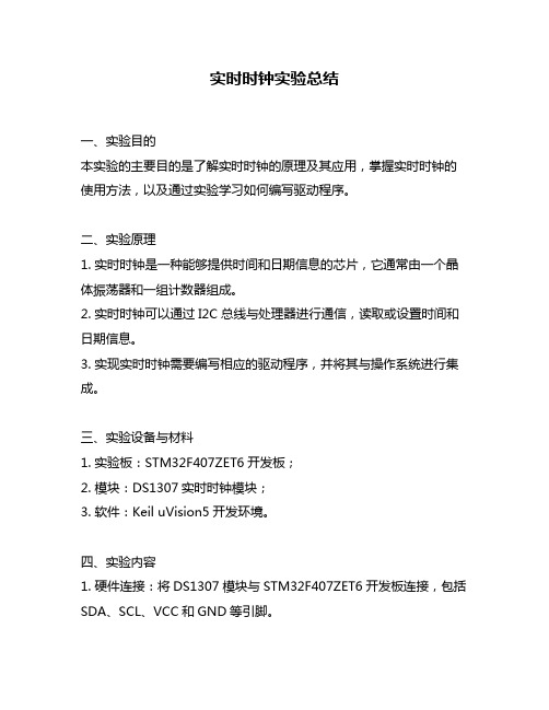
§2:引脚与接线DS1307 典型接线如图 1 所示。
BT1 为备用电池,3V,7 脚为方波输出,通常把该脚接到单片机的能够产生电平变化中断的引脚,如设置成每秒输出1个方波,则会每秒中断一次,读取时间用以显示。
图1中的R1、R2、R4是必须的上拉电阻。
图 1 DS1307典型接线图§3:DS1307 RAMDS1307 寄存器统一编址,其中的时间相关的和寄器数据组织格式如表 1。
表1时间相关的寄存器说明注:存放时的单元02的位6为12/24小时设置位,1为12时制,0为24时制。
位5为上午/下午(AM/PM)指示位,0为上午(AM),1为下午(PM),在24时制中,该位为10倍时位。
在读写过程中DS1307内部有一个地址指针,通过写操作可对它赋值,读和写每一字节时自动加一,当指针越过DS1307内部RAM尾时指针将返回到0地址处。
DS1307 的时钟和日历数据按 BCD 码存储。
§4:方波信号输出功能方波信号输出功能从SQW/OUT引脚输出设置频率的方波,CONTROL寄存器用于控制SQW/OUT脚的输出,其地址为07,每位的内容如表2。
表2CONTROL寄存器位BIT7(OUT):此位表示在方波输出被禁止时(BIT4=0),SQW/OUT 引脚的逻辑电平,在BIT4=0(SQWE=0方波输出禁止)时,若BIT7(OUT)为1则SQL/OUT引脚为高电平,反之亦然。
BIT4(SQWE)方波输出允许/禁止控制位,SQWE =1 允许方波输出(有效);BIT4=0禁止方波输出。
BIT0(RS0)、BIT1(RS1)于设定输出波形的频率,如表 3。
表 3 CONTROL寄存器说明由于DS1307的方波输出脚为集电极开路,故要在外部加上上拉电阻!要注意的是,00h地址的第7位为器件时钟允许位(CH),此位为1则芯片未开始工作,即时钟未走时,所以在上电时单片机要先读出秒,并判断位7(CH)是否为1,如为 1 要把该位清零写入秒寄存器(地址为 0),并把其他的时间单元设定为默认值。
一种电子数显时钟的制作方法
一种电子数显时钟的制作方法简介电子数显时钟是使用数字和电子元件来显示时间的一种普遍存在的时钟。
制作一般的电子数显时钟通常需要一些基本的电子技能。
本文将介绍一种较为简单的电子数显时钟制作方法,不需要太高的技能门槛,也可以用于初学者进行制作。
所需工具和材料•数码钟芯片:常见的数码芯片有DS1302、DS1307等型号,本文中将采用DS1302芯片;•LED数码管:一般需要4位和7段LED数码管,也可以根据需要选择更多的位数;•电子元器件:–电容:22pF * 2、100nF * 1、10uF * 1;–电阻:1kΩ * 2、10kΩ * 1、4.7kΩ * 1;–钽电容:2.2uF * 1;–晶体管:2N3904 * 1、2N3906 * 1;–二极管:1N4007 * 1;•面包板、电源线等基本工具材料。
程序设计本文中的程序采用C语言,可以在芯片中下载和存储。
下面给出基本的程序框图和说明。
#include <DS1302.h> // 导入DS1302芯片的库// 数码管引脚定义#define DS 11#define ST 10#define SH 9#define A 2#define B 3#define C 4#define D 5#define E 6#define F 7#define G 8int year, month, day, week, hour, minute, second; //定义年、月、日、星期、小时、分钟、秒void setup() {// 数码管引脚定义为输出pinMode(DS, OUTPUT);pinMode(ST, OUTPUT);pinMode(SH, OUTPUT);pinMode(A, OUTPUT);pinMode(B, OUTPUT);pinMode(C, OUTPUT);pinMode(D, OUTPUT);pinMode(E, OUTPUT);pinMode(F, OUTPUT);pinMode(G, OUTPUT);// 初始化DS1302芯片DS1302_init();// 设置初始时间DS1302_set_time(20, 6, 21, 3, 11, 59, 45); // 年、月、日、星期、小时、分钟、秒}void loop() {// 获取当前时间year = DS1302_get_year();month = DS1302_get_month();day = DS1302_get_day();week = DS1302_get_week();hour = DS1302_get_hour();minute = DS1302_get_minute();second = DS1302_get_second();// 将显示时间转换为BCD码int y0 = year % 10;int y1 = year / 10;int m0 = month % 10;int m1 = month / 10;int d0 = day % 10;int d1 = day / 10;int h0 = hour % 10;int h1 = hour / 10;int mi0 = minute % 10;int mi1 = minute / 10;int s0 = second % 10;int s1 = second / 10;// 显示年份digitalWrite(DS, LOW);shiftOut(SH, ST, MSBFIRST, B00111111); // 关闭所有数码管digitalWrite(DS, HIGH);digitalWrite(DS, LOW);shiftOut(SH, ST, MSBFIRST, B00000100); // 选择第一位数码管digitalWrite(DS, HIGH);digitalWrite(DS, LOW);shiftOut(SH, ST, MSBFIRST, y1 == 0 ? B00000000 : dig it[y1]); // 如果高位为0,则不显示digitalWrite(DS, HIGH);digitalWrite(DS, LOW);shiftOut(SH, ST, MSBFIRST, digit[y0]); // 显示低位 digitalWrite(DS, HIGH);// 显示月份...// 显示日、星期...// 显示小时...// 显示分钟...// 显示秒...}程序的具体实现可根据需要进行调节。
实时时钟芯片 DS1302 介绍

实时时钟芯片DS1302 介绍
DS1302 是个实时时钟芯片,我们可以用单片机写入时间或者读取当前的时间数据,下面带着大家通过阅读这个芯片的数据手册来学习和掌握这个器件。
由于IT 技术国际化比较强,因此数据手册绝大多数都是英文的,导致很多英语基础不好的同学看到英文手册头就大了。
这里我要告诉大家的是,只要精神不退缩,方法总比困难多,很多英语水平不高的,看数据手册照样完全没问题,因为我们用到的专业词汇也就那么几个,多看几次就认识了。
我们现在不是考试,因此大家可以充分利用一些英文翻译软件,翻译过来的中文意思有时候可能不是那么准确,那你就把翻译的内容和英文手册里的一些图表比较参考学习。
此外数据手册除了介绍性的说明外,一般还会配相关的图形或者表格,结合起来看也有利于理解手册所表达的意思。
这节课我会把DS1302 的英文资料尽可能的用比较便于理解的方式给大家表达出来,同学们可以把我的表达和英文手册多做一下对比,尽可能快的开始学会了解英文手册。
DS1302 的特点DS1302 是DALLAS(达拉斯)公司推出的一款涓流充电时钟芯片,2001 年DALLAS 被MAXIM(美信)收购,因此我们看到的DS1302 的数据手册既有DALLAS 的标志,又有MAXIM 的标志,大家了解即可。
DS1302 实时时钟芯片广泛应用于电话、传真、便携式仪器等产品领域,它的主要性能指标如下:
1)DS1302 是一个实时时钟芯片,可以提供秒、分、小时、日期、月、年等信息,并且还有软件自动调整的能力,可以通过配置AM/PM 来决定采用24 小时格式还是12 小时格式。
实时时钟电路DS1302芯片的原理及应用

实时时钟电路DS1302芯片的原理及应用DS1302芯片是一种低功耗的实时时钟(RTC)电路。
它包含了一个真正的时钟/日历芯片和31个静态RAM存储单元,用于存储时钟和日期信息。
DS1302芯片的工作电压范围为2.0V至5.5V,并且具有极低的功耗,非常适合于移动电子设备和电池供电的应用。
DS1302芯片的原理如下:1.时钟发生器:DS1302芯片内部具有一个实时时钟发生器,它通过晶振和电容电路生成稳定的振荡信号,用于计时。
2.时钟/计时电路:DS1302芯片内部的时钟/计时电路可以精确地计算并保持当前的时间和日期。
它具有秒、分钟、小时、日期、月份、星期和年份等不同的计时单元。
3.RAM存储单元:DS1302芯片包含31个静态RAM存储单元,用于存储时钟和日期信息。
这些存储单元可以通过SPI接口进行读写操作,并且在断电情况下也能够保持数据。
4.控制接口:DS1302芯片通过3线接口与微控制器通信,包括一个时钟线、一个数据线和一个使能线。
这种接口使得与微控制器的通信非常简单,并且能够高效地读写时钟和日期信息以及控制芯片的其他功能。
DS1302芯片的应用如下:1.实时时钟:DS1302芯片可以用作电子设备中的实时时钟。
例如,它可以用于计算机、嵌入式系统、电子游戏等设备中,以提供准确的时间和日期信息。
2.定时器:DS1302芯片的计时功能可以用于设计各种定时器应用。
例如,它可以用于计时器、倒计时器、定时开关等应用中,以实现定时功能。
3.时钟显示:DS1302芯片可以与显示模块结合使用,用于显示当前的时间和日期。
例如,它可以用于数字钟、计时器、时钟频率计等应用中。
4.能量管理:由于DS1302芯片具有低功耗特性,因此它可以用于电池供电的设备中,以实现节能的能量管理策略。
例如,它可以用于手持设备、无线传感器网络等应用中,以延长电池寿命。
综上所述,DS1302芯片是一种低功耗的实时时钟电路,具有精确计时、可靠存储和简单接口等优点,适用于计时、显示和能量管理等各种应用中。
ds1307数字时钟课程设计

ds1307数字时钟课程设计一、课程目标知识目标:1. 理解DS1307实时时钟芯片的基本原理和功能;2. 掌握读取和设置DS1307时间参数的方法;3. 学会通过编程实现数字时钟显示的基本技巧。
技能目标:4. 能够正确连接DS1307实时时钟模块与微控制器;5. 能够编写程序读取DS1307时间数据,并在LCD显示屏上显示;6. 能够诊断和解决数字时钟显示中的常见问题。
情感态度价值观目标:7. 培养学生对电子产品的探索精神和实践能力;8. 强化学生合作学习、分享成果的团队意识;9. 激发学生将理论知识应用于实践的兴趣,增强其对科学技术的认识与尊重。
本课程设计针对中学生电子技术课程,结合DS1307数字时钟的制作,旨在通过实践操作,帮助学生掌握基础电子元件的使用和程序编写,同时培养学生的动手能力和创新思维。
课程目标设定符合学生好奇心强、动手欲望高的特点,同时满足学科教学要求,将理论与实践相结合,为学生的后续学习打下坚实基础。
二、教学内容本节教学内容围绕DS1307数字时钟的制作展开,主要包括以下部分:1. 实时时钟芯片DS1307的基础知识:介绍DS1307的内部结构、工作原理及主要性能参数,关联教材第三章第二节。
2. 硬件连接与接口:讲解DS1307与微控制器(如Arduino)的硬件连接方法,包括VCC、GND、I2C接口等,对应教材第三章第三节。
3. I2C通信协议:介绍I2C通信协议的基本原理,以及如何在微控制器上实现I2C通信,关联教材第二章第五节。
4. DS1307时间读取与设置:详细讲解如何通过编程读取和设置DS1307的时间参数,包括时、分、秒、日期等,对应教材第三章第四节。
5. 数字时钟显示编程:教授如何将读取到的DS1307时间数据实时显示在LCD显示屏上,涉及编程技巧及调试方法,关联教材第四章第一节。
6. 故障诊断与排除:介绍在数字时钟制作过程中可能遇到的常见问题及解决方法,强化学生的实际操作能力,对应教材第四章第二节。
基于DS1307的简易时钟显示程序分享

基于DS1307的简易时钟显示程序分享
目前家用的数字电子钟,多数只能显示小时、分钟等信息,功能单一,而且大都采用LED数码管作为显示器件,功耗大,不能令消费者满意。
DS1307简介AM/PM 标志位决定时钟工作于24小时或12小时模式,芯片有一个内置的电源感应电路,具有掉电检测和电池切换功能。
是一款低功耗,具有56字节非失性RAM的全BCD码时钟日历实时时钟芯片,地址和数据通过两线双向的串行总线的传输,芯片可以提供秒,分,小时等信息,每一个月的天数能自动调整。
并且有闰年补偿功能
特点:
可对秒,时,分,每月的天数,月份,每周的天数进行计数,并具有闰年补偿功能。
计年上限2100。
56字节非失性的RAM
两线串行接口
可编程方波输出
自动掉电检测和切换电路
在电池备份模式下,功耗小于500nA
工业级的工作温度:-40 到80
8脚DIP和SOIC封装
* Coder:NUIST_XKFYT
* E-mail:weilun_fong@(Welcome to get help info about this program)
* Date:2016-7-17
*
* Device:STC89C54RD,DS1307Z+
* FuncTIon:简易时钟显示
* Note:。
- 1、下载文档前请自行甄别文档内容的完整性,平台不提供额外的编辑、内容补充、找答案等附加服务。
- 2、"仅部分预览"的文档,不可在线预览部分如存在完整性等问题,可反馈申请退款(可完整预览的文档不适用该条件!)。
- 3、如文档侵犯您的权益,请联系客服反馈,我们会尽快为您处理(人工客服工作时间:9:00-18:30)。
FEATURESReal time clock counts seconds, minutes,hours, date of the month, month, day of the week, and year with leap year compensation valid up to 210056 byte nonvolatile RAM for data storage 2-wire serial interfaceProgrammable squarewave output signal Automatic power-fail detect and switch circuitryConsumes less than 500 nA in battery backup mode with oscillator runningOptional industrial temperature range -40°C to +85°CAvailable in 8-pin DIP or SOICRecognized by Underwriters LaboratoryORDERING INFORMATIONDS1307 8-Pin DIP DS1307Z 8-Pin SOIC (150 mil)DS1307N 8-Pin DIP (Industrial)DS1307ZN 8-Pin SOIC (Industrial)PIN ASSIGNMENTPIN DESCRIPTIONV CC - Primary Power Supply X1, X2 - 32.768 kHz Crystal Connection V BAT - +3V Battery Input GND - Ground SDA - Serial Data SCL - Serial ClockSQW/OUT - Square wave/Output DriverDESCRIPTIONThe DS1307 Serial Real Time Clock is a low power, full BCD clock/calendar plus 56 bytes of nonvolatile SRAM. Address and data are transferred serially via a 2-wire bi-directional bus. The clock/calendar provides seconds, minutes, hours, day, date, month, and year information. The end of the month date is automatically adjusted for months with less than 31 days, including corrections for leap year. The clock operates in either the 24-hour or 12-hour format with AM/PM indicator. The DS1307has a built-in power sense circuit which detects power failures and automatically switches to the battery supply.DS130764 X 8 Serial Real Time ClockOPERATIONThe DS1307 operates as a slave device on the serial bus. Access is obtained by implementing a START condition and providing a device identification code followed by a register address. Subsequent registers can be accessed sequentially until a STOP condition is executed. When V CC falls below 1.25 x V BAT the device terminates an access in progress and resets the device address counter. Inputs to the device will not be recognized at this time to prevent erroneous data from being written to the device from an out of tolerance system. When V CC falls below V BAT the device switches into a low current battery backup mode. Upon power up, the device switches from battery to V CC when V CC is greater than V BAT+0.2V and recognizes inputs when V CC is greater than 1.25 x V BAT. The block diagram in Figure 1 shows the main elements of the Serial Real Time Clock.DS1307 BLOCK DIAGRAM Figure 1SIGNAL DESCRIPTIONSV CC, GND - DC power is provided to the device on these pins. V CC is the +5 volt input. When 5 volts is applied within normal limits, the device is fully accessible and data can be written and read. When a 3-volt battery is connected to the device and V CC is below 1.25 x V BAT, reads and writes are inhibited. However, the Timekeeping function continues unaffected by the lower input voltage. As V CC falls below V BAT the RAM and timekeeper are switched over to the external power supply (nominal 3.0V DC) at V BAT.V BAT- Battery input for any standard 3-volt lithium cell or other energy source. Battery voltage must be held between 2.0 and 3.5 volts for proper operation. The nominal write protect trip point voltage at which access to the real time clock and user RAM is denied is set by the internal circuitry as 1.25 x V BAT nominal. A lithium battery with 48 mAhr or greater will back up the DS1307 for more than 10 years in the absence of power at 25 degrees C.SCL (Serial Clock Input) - SCL is used to synchronize data movement on the serial interface.SDA (Serial Data Input/Output) - SDA is the input/output pin for the 2-wire serial interface. The SDA pin is open drain which requires an external pullup resistor.SQW/OUT (Square Wave/ Output Driver) - When enabled, the SQWE bit set to 1, the SQW/OUT pin outputs one of four square wave frequencies (1 Hz, 4 kHz, 8 kHz, 32 kHz). The SQW/OUT pin is open drain which requires an external pullup resistor. SQW/OUT will operate with either Vcc or Vbat applied.X1, X2 - Connections for a standard 32.768 kHz quartz crystal. The internal oscillator circuitry is designed for operation with a crystal having a specified load capacitance (CL) of 12.5 pF.For more information on crystal selection and crystal layout considerations, please consult Application Note 58, “Crystal Considerations with Dallas Real Time Clocks.” The DS1307 can also be driven by an external 32.768 kHz oscillator. In this configuration, the X1 pin is connected to the external oscillator signal and the X2 pin is floated.Please review Application Note 95, “Interfacing the DS1307 with a 8051-Compatible Microcontroller”for additional information.RTC AND RAM ADDRESS MAPThe address map for the RTC and RAM registers of the DS1307 is shown in Figure 2. The real time clock registers are located in address locations 00h to 07h. The RAM registers are located in address locations 08h to 3Fh. During a multi-byte access, when the address pointer reaches 3Fh, the end of RAM space, it wraps around to location 00h, the beginning of the clock space.DS1307 ADDRESS MAP Figure 2CLOCK AND CALENDARThe time and calendar information is obtained by reading the appropriate register bytes. The real time clock registers are illustrated in Figure 3. The time and calendar are set or initialized by writing the appropriate register bytes. The contents of the time and calendar registers are in the Binary-Coded Decimal (BCD) format. Bit 7 of Register 0 is the Clock Halt (CH) bit. When this bit is set to a 1, the oscillator is disabled. When cleared to a 0, the oscillator is enabled.Please note that the initial power on state of all registers is not defined. Therefore it is important to enable the oscillator (CH bit=0) during initial configuration.00H07H 08H 3FHThe DS1307 can be run in either 12-hour or 24-hour mode. Bit 6 of the hours register is defined as the 12- or 24-hour mode select bit. When high, the 12-hour mode is selected. In the 12-hour mode, bit 5 is the AM/PM bit with logic high being PM. In the 24-hour mode, bit 5 is the second 10 hour bit (20-23 hours).On a 2-wire START, the current time is transferred to a second set of registers. The time information is read from these secondary registers, while the clock may continue to run. This eliminates the need to re-read the registers in case of an update of the main registers during a read.DS1307 TIMEKEEPER REGISTERS Figure 3CONTROL REGISTERThe DS1307 Control Register is used to control the operation of the SQW/OUT pin.BIT 7BIT 6BIT 5BIT 4BIT 3BIT 2BIT 1BIT 0 OUT X X SQWE X X RS1RS0OUT (Output control): This bit controls the output level of the SQW/OUT pin when the square wave output is disabled. If SQWE=0, the logic level on the SQW/OUT pin is 1 if OUT=1 and is 0 if OUT=0.SQWE (Square Wave Enable): This bit, when set to a logic 1, will enable the oscillator output. The frequency of the square wave output depends upon the value of the RS0 and RS1 bits.RS (Rate Select): These bits control the frequency of the square wave output when the square wave output has been enabled. Table 1 lists the square wave frequencies that can be selected with the RS bits. SQUAREWAVE OUTPUT FREQUENCY Table 1RS1RS0SQW OUTPUTFREQUENCY001Hz01 4.096 kHz108.192 kHz1132.768 kHz2-WIRE SERIAL DATA BUSThe DS1307 supports a bi-directional 2-wire bus and data transmission protocol. A device that sends data onto the bus is defined as a transmitter and a device receiving data as a receiver. The device that controls the message is called a master. The devices that are controlled by the master are referred to as slaves. The bus must be controlled by a master device which generates the serial clock (SCL), controls the bus access, and generates the START and STOP conditions. The DS1307 operates as a slave on the 2-wire bus. A typical bus configuration using this 2-wire protocol is show in Figure 4.TYPICAL 2-WIRE BUS CONFIGURATION Figure 4Figures 5, 6, and 7 detail how data is transferred on the 2-wire bus.Data transfer may be initiated only when the bus is not busy.During data transfer, the data line must remain stable whenever the clock line is HIGH. Changes in the data line while the clock line is high will be interpreted as control signals.Accordingly, the following bus conditions have been defined:Bus not busy: Both data and clock lines remain HIGH.Start data transfer: A change in the state of the data line, from HIGH to LOW, while the clock is HIGH, defines a START condition.Stop data transfer: A change in the state of the data line, from LOW to HIGH, while the clock line is HIGH, defines the STOP condition.Data valid: The state of the data line represents valid data when, after a START condition, the data line is stable for the duration of the HIGH period of the clock signal. The data on the line must be changed during the LOW period of the clock signal. There is one clock pulse per bit of data.Each data transfer is initiated with a START condition and terminated with a STOP condition. The number of data bytes transferred between START and STOP conditions is not limited, and is determined by the master device. The information is transferred byte-wise and each receiver acknowledges with a ninth bit. Within the 2-wire bus specifications a regular mode (100 kHz clock rate) and a fast mode (400 kHz clock rate) are defined. The DS1307 operates in the regular mode (100 kHz) only.Acknowledge: Each receiving device, when addressed, is obliged to generate an acknowledge after the reception of each byte. The master device must generate an extra clock pulse which is associated with this acknowledge bit.A device that acknowledges must pull down the SDA line during the acknowledge clock pulse in such a way that the SDA line is stable LOW during the HIGH period of the acknowledge related clock pulse. Of course, setup and hold times must be taken into account. A master must signal an end of data to the slave by not generating an acknowledge bit on the last byte that has been clocked out of the slave. In this case, the slave must leave the data line HIGH to enable the master to generate the STOP condition.DATA TRANSFER ON 2-WIRE SERIAL BUS Figure 5Depending upon the state of the R/W bit, two types of data transfer are possible:1.Data transfer from a master transmitter to a slave receiver. The first byte transmitted by themaster is the slave address. Next follows a number of data bytes. The slave returns an acknowledge bit after each received byte. Data is transferred with the most significant bit (MSB) first.2.Data transfer from a slave transmitter to a master receiver. The first byte (the slave address) istransmitted by the master. The slave then returns an acknowledge bit. This is followed by the slave transmitting a number of data bytes. The master returns an acknowledge bit after all received bytes other than the last byte. At the end of the last received byte, a ’not acknowledge’ is returned.The master device generates all of the serial clock pulses and the START and STOP conditions. A transfer is ended with a STOP condition or with a repeated START condition. Since a repeated START condition is also the beginning of the next serial transfer, the bus will not be released. Data is transferred with the most significant bit (MSB) first.The DS1307 may operate in the following two modes:1.Slave receiver mode (DS1307 write mode): Serial data and clock are received through SDA andSCL. After each byte is received an acknowledge bit is transmitted. START and STOP conditions are recognized as the beginning and end of a serial transfer. Address recognition is performed by hardware after reception of the slave address and *direction bit (See Figure 6). The address byte is the first byte received after the start condition is generated by the master. The address byte contains the 7 bit DS1307 address, which is 1101000, followed by the *direction bit (R/W) which, for a write, is a 0. After receiving and decoding the address byte the device outputs an acknowledge on the SDA line. After the DS1307 acknowledges the slave address + write bit, the master transmits a register address to the DS1307 This will set the register pointer on the DS1307. The master will then begin transmitting each byte of data with the DS1307 acknowledging each byte received. The master will generate a stop condition to terminate the data write.DATA WRITE - SLAVE RECEIVER MODE Figure 62.Slave transmitter mode (DS1307 read mode): The first byte is received and handled as in the slavereceiver mode. However, in this mode, the *direction bit will indicate that the transfer direction is reversed. Serial data is transmitted on SDA by the DS1307 while the serial clock is input on SCL.START and STOP conditions are recognized as the beginning and end of a serial transfer (See Figure 7). The address byte is the first byte received after the start condition is generated by the master. The address byte contains the 7-bit DS1307 address, which is 1101000, followed by the *direction bit (R/W) which, for a read, is a 1. After receiving and decoding the address byte the device inputs an acknowledge on the SDA line. The DS1307 then begins to transmit data starting with the register address pointed to by the register pointer. If the register pointer is not written to before the initiation of a read mode the first address that is read is the last one stored in the register pointer. The DS1307 must receive a Not Acknowledge to end a read.DATA READ - SLAVE TRANSMITTER MODE Figure 7ABSOLUTE MAXIMUM RATINGS*Voltage on Any Pin Relative to Ground -0.5V to +7.0VOperating Temperature 0°C to 70°C (-40°C to 85°C for industrial)Storage Temperature -55°C to +125°CSoldering Temperature 260°C for 10 seconds DIPSee JPC/JEDEC Standard J-STD-020A forSurface Mount Devices*This is a stress rating only and functional operation of the device at these or any other conditions above those indicated in the operation sections of this specification is not implied. Exposure to absolute maximum rating conditions for extended periods of time may affect reliability. RECOMMENDED DC OPERATING CONDITIONS(0°C to 70°C or -40°C to +85°C) PARAMETER SYMBOL MIN TYP MAX UNITS NOTES Supply Voltage V CC 4.5 5.0 5.5V1 Logic 1V IH 2.2V CC+0.3V1 Logic 0V IL-0.3+0.8V1V BAT Battery Voltage V BAT 2.0 3.5V1 DC ELECTRICAL CHARACTERISTICS(0°C to 70°C or -40°C to +85°C; V CC=4.5V to 5.5V) PARAMETER SYMBOL MIN TYP MAX UNITS NOTES Input Leakage I LI1µA10I/O Leakage I LO1µA11 Logic 0 Output V OL0.4V2 Active Supply Current I CCA 1.5mA9 Standby Current I CCS200µA3I BAT1300500nA4 Battery Current (OSC ON);SQW/OUT OFFI BAT2480800nA4 Battery Current (OSC ON);SQW/OUT ON (32 kHz)AC ELECTRICAL CHARACTERISTICS(0°C to 70°C or -40°C to +85°C; V CC=4.5V to 5.5V) PARAMETER SYMBOL MIN TYP MAX UNITS NOTES SCL Clock Frequency f SCL0100kHzBus Free Time Between a STOP andt BUF 4.7µsSTART ConditionHold Time (Repeated) START Condition t HD:STA 4.0µs5 LOW Period of SCL Clock t LOW 4.7µsHIGH Period of SCL Clock t HIGH 4.0µst SU:STA 4.7µsSet-up Time for a Repeated STARTConditionData Hold Time t HD:DAT0µs6, 7 Data Set-up Time t SU:DAT250nsRise Time of Both SDA and SCL Signals t R1000nsFall Time of Both SDA and SCL Signals t F300nsSet-up Time for STOP Condition t SU:STO 4.7µsCapacitive Load for each Bus Line C B400pF8I/O Capacitance C I/O10pFCrystal Specified Load Capacitance12.5pF NOTES:1.All voltages are referenced to ground.2.Logic zero voltages are specified at a sink current of 5 mA at V CC=4.5V, V OL=GND for capacitiveloads.3.I CCS specified with V CC=5.0V and SDA, SCL=5.0V.4.V CC=0V, V BAT=3V.5.After this period, the first clock pulse is generated.6. A device must internally provide a hold time of at least 300 ns for the SDA signal (referred to theV IHMIN of the SCL signal) in order to bridge the undefined region of the falling edge of SCL.7.The maximum t HD:DAT has only to be met if the device does not stretch the LOW period (t LOW) of theSCL signal.8.C B - total capacitance of one bus line in pF.9.I CCA - SCL clocking at max frequency = 100 kHz.10.SCL only.11.SDA and SQW/OUTTIMING DIAGRAM Figure 8DS1307 64 X 8 SERIAL REAL TIME CLOCK 8-PIN DIP MECHANICAL DIMENSIONSPKG 8-PIN DIM MIN MAX A IN.MM 0.3609.140.40010.16B IN.MM 0.2406.100.2606.60C IN.MM 0.1203.050.1403.56D IN.MM 0.3007.620.3258.26E IN.MM 0.0150.380.0401.02F IN.MM 0.1203.040.1403.56G IN.MM 0.0902.290.1102.79H IN.MM 0.3208.130.3709.40J IN.MM 0.0080.200.0120.30K IN.MM0.0150.380.0210.53DS130711 of 11DS1307Z 64 X 8 SERIAL REAL TIME CLOCK8-PIN SOIC (150-MIL) MECHANICAL DIMENSIONS PKG8-PIN (150 MIL)DIMMIN MAX A IN.MM0.1884.780.1964.98B IN.MM0.1503.810.1584.01C IN.MM0.0481.220.0621.57E IN.MM0.0040.100.0100.25F IN.MM0.0531.350.0691.75G IN.MM0.050 BSC 1.27 BSC H IN.MM0.2305.840.2446.20J IN.MM0.0070.180.0110.28K IN.MM0.0120.300.0200.51L IN.MM0.0160.410.0501.27phi 0°8°56-G2008-001 - Free Datasheet Search Engine。